

Page 1
SATELLITESOUNDAND VIDEO PROCESSOR
SOUND
.
TWO INDEPENDENT SOUND DEMODULATORS
.
PLL DEMODULATION WITH 5-10MHz FREQUENCYSYNTHESIS
.
PROGRAMMABLE FM DEMODULATOR
BANDWIDTH ACCOMODATING FM DEVIATIONSFROM ±30kHz TILL ±400kHz
.
PROGRAMMABLE 50/75µs, J17 OR NO DEEMPHASIS
.
WEGENERPANDASYSTEM
.
TWO AUXILIARYAUDIOINPUTS AND OUTPUTS
.
GAIN CONTROLLED AND MUTEABLE
AUDIOOUTPUTS
.
HIGH IMPEDANCE MODE AUDIO OUTPUTS
FORTWINTUNERAPPLICATIONS
VIDEO
.
COMPOSITE VIDEO 6-bit 0 to 12.7dB GAIN
CONTROL
.
COMPOSITEVIDEOSELECTABLEINVERTER
.
TWO SELECTABLE VIDEO DE-EMPHASIS
NETWORKS
.
6 x 3 VIDEOMATRIX
.
BLACK LEVEL ADJUSTABLE OUTPUT FOR
ON-BOARDVIDEOCRYPTDECODER
.
HIGH IMPEDANCE MODE VIDEO OUTPUTS
FORTWINTUNERAPPLICATIONS
MISCELLANEOUS
.
22kHzTONEGENERA TI ONFORLNBCONTROL
.
I2C BUSCONTROL
CHIPADDRESSES= 06
.
LOW POWER STAND-BY MODE WITH ACTIVEAUDIOANDVIDEO MATRIXES
HEX
OR46
HEX
STV0056AF
TQFP64 (10 x 10mm)
(Thin Plastic Quad Flat Pack)
ORDER CODE : STV0056AF
DESCRIPTION
TheSTV0056AFBICMOSintegratedcircuit realizes
allthenecessarysignalprocessingfromthetunerto
theAudio/Videoinputandoutputconnectorsregardlessthe satellitesystem.
February 1998
1/27
Page 2
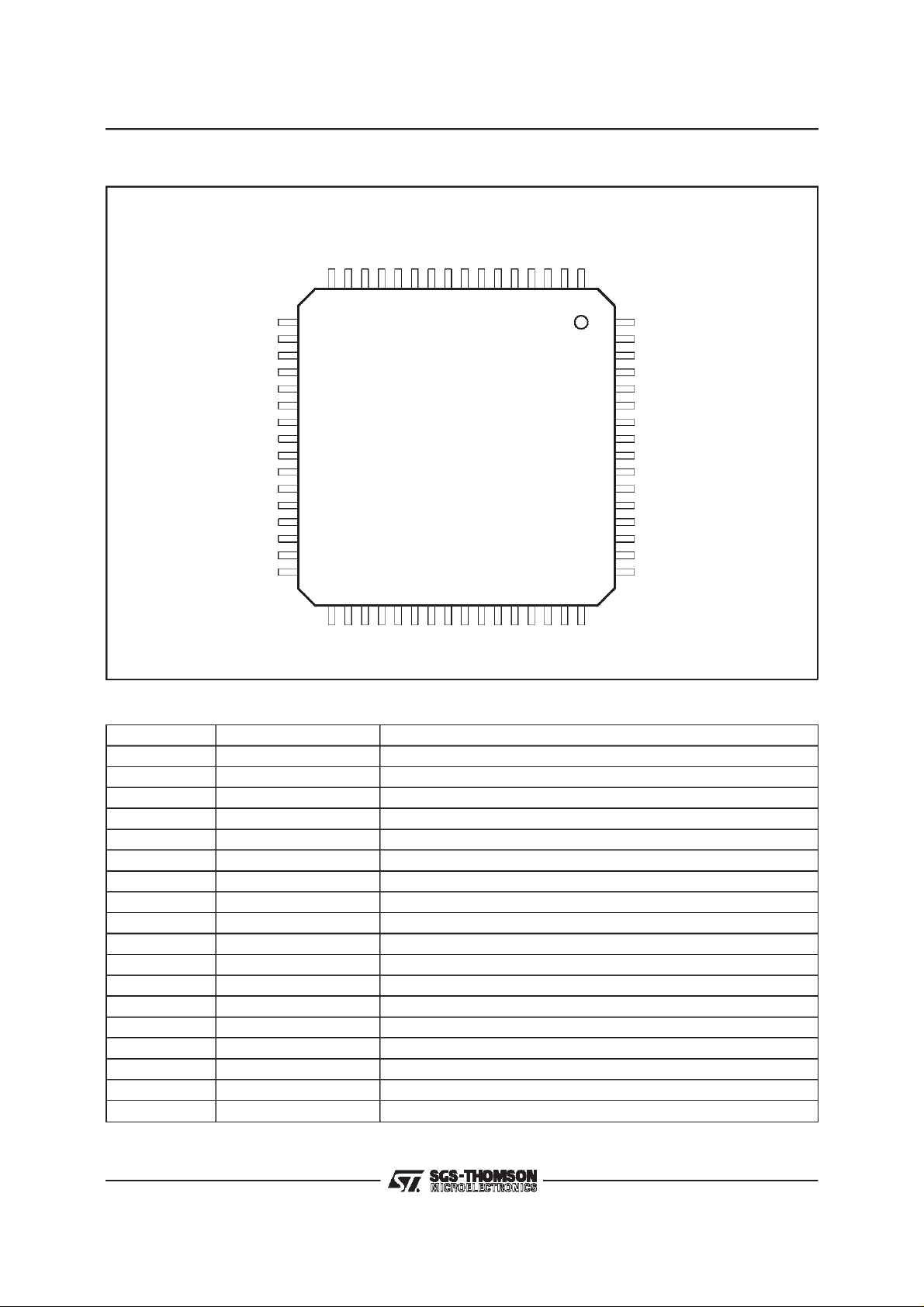
STV0056AF
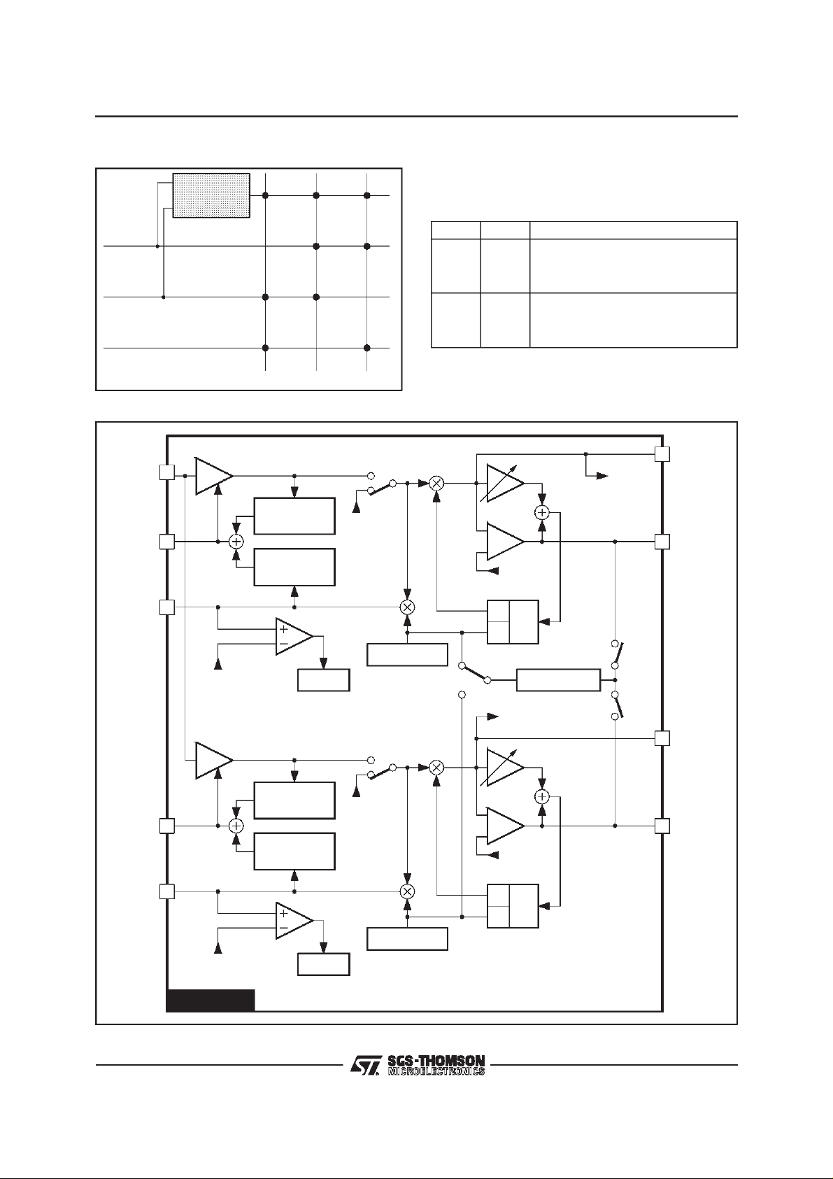
PIN CONNECTIONS
GND
S2 VID OUT
VOL L
S2 VID RTN
S2 OUTL
CLAMP IN
S2 OUTR
UNCL DEEM
VIDEEM2/22kHz
V 12V
V 12V
VIDEEM1
VGND
VGND
NC
B-BAND IN
S2 RTN L
S2 RTNR
FM IN
S3 RTN L
S3 RTNR
AGC L
S3 OUT L
S3 OUTR
SCL
SDA
HA
J17 R
J17 L
XTL
V
DD
1213141516
17
18
19
20
21
22
23
24
25
IO
26
27
28
29
30
31
32
5V
38 39 40 41 42 43 44 45 46 47 4833 34 35 36 37
NC
GND 5V
U75 L
DET L
CPUMP L
NC
AGC R
AMPLKL
REF
V
A 12V
AGND L
AGND L
A 12V
1234567891011
DET R
AMPLK R
PIN ASSIGNMENT
Pin Number Name Function
1 GND Connected to the Lead Frame
2 S2 VID OUT VCR-Scart 2 VideoOutput
3 VOL L Volume Controlled Audio Out Left
4 S2 VID RTN VCR-Scart 2 Video Return
5 S2 OUT L Fixed Level Audio OutputLeft (to VCR)
6 CLAMP IN Sync-Tip Clamp Input
7 S2 OUT R Fixed Level Audio OutputRight (to VCR)
8 UNCL DEEM Unclamped Deemphasized Video Output
9 VIDEEM2/22kHz Video Deemphasis 2 or 22kHz Output
10 - 11 V 12V Video 12V Supply
12 VIDEEM1 Video Deemphasis 1
13 - 14 V GND Video Ground
15 NC
16 B-BAND IN Base Band Input
17 S2 RTN L Auxiliary Audio Return Left (from VCR)
18 S2 RTN R Auxiliary Audio Return Right (from VCR)
19 FM IN FM Demodulator Input
20 S3 RTN L Auxiliary Audio Return Left (from decoder)
64
S1 VIDOUT
63
S3 VIDOUT
62
VOL R
61
S3 VIDRTN
60
S1 VIDRTN
59
LEVELR
58
PKIN R
57
FCR
56
AGNDR
55
FCL
54
PKIN L
53
LEVELL
52
PKOUTL
51
PKOUTR
50
I
49
U75 R
REF
CPUMPR
0056F-01.EPS
0056F-01.TBL
2/27
Page 3

PIN ASSIGNMENT(continued)
Pin Number Name Function
21 S3 RTN R Auxiliary Audio Return Right (from decoder)
22 AGC L AGC Peak Detector Capacitor Left
23 S3 OUT L Auxiliary Audio Output L (to decoder)
24 S3 OUT R Auxiliary Audio Output R (to decoder)
25 I/O/22kHz Digital Input/Output or 22kHz Output
26 SCL I
27 SDA I
28 HA Hardware Address
29 J17 R J17 Deemphasis Time Constant Right
30 J17 L J17 Deemphasis Time Constant Left
31 XTL 4/8MHz Quartz Crystal or Clock Input
32 V
5V Digital 5V Power Supply
DD
34 NC Not Connected
33 GND 5V Digital Power Ground
35 CPUMP L FM PLL Charge Pump Capacitor Left
36 DET L FM PLL Filter Left
37 U75 L Deemphasis Time Constant Left
38 AMPLK L Amplitude Detector Capacitor Left
39 AGC R AGC Peak Detector Capacitor Right
40 NC
41 - 42 A GND L Audio Ground
43 V
REF
44 - 45 A 12V Audio 12V Supply
46 AMPLK R Amplitude Detector Capacitor Left
47 DET R FM PLL Filter Right
48 U75 R Deemphasis Time Constant Right
49 CPUMP R FM PLL Charge Pump Capacitor Right
50 I
REF
51 PK OUT R Noise Reduction Peak Detector Output Right
52 PK OUT L Noise Reduction Peak Detector Output Left
53 LEVEL L Noise Reduction Level Left
54 PK IN L Noise Reduction Peak Detector Input
55 FC L Audio Roll-off Left
56 A GND R Audio Ground
57 FC R Audio Roll-off Right
58 PK IN R Noise Reduction Peak Detector Input Right
59 LEVEL R Noise Reduction Level Right
60 S1 VID RTN TV-Scart 1 Video Return
61 S3 VID RTN Decoder-Scart Video Return
62 VOL R Volume Controlled Audio Out Right
63 S3 VID OUT Decoder-Scart Video Output
64 S1 VID OUT TV-Scart 1 VideoOutput
2
C Bus Clock
2
C Bus Data
2.4V Reference
Current Reference Resistor
STV0056AF
0056F-01.TBL
3/27
Page 4

STV0056AF
PIN DESCRIPTION
1 - Sound Detection
FMIN
This is the input to the two FM demodulators. It
feeds two AGC amplifiers with a bandwidth of at
least 5-10MHz. There is one amplifier for each
channelboth withthe sameinput. TheAGC amplifiers have a 0dB to +40dBrange.
=5kΩ, Mininput = 2mVPPper subcarrier.
Z
IN
Max input = 500mV
addedtogether,when their phases coincide).
AGC L, AGC R
AGC amplifiers peak detector capacitor connections.The output current hasan attack/decayratio
of 1:32. That is the ramp up current is approximately 5µA and decay current is approximately
160µA. 11V gives maximum gain. These pins are
also driven by a circuit monitoring the voltage on
AMPLKL and AMPLK R respectively.
AMPLKL, AMPLK R
The outputs of amplitude detectors LEFT and
RIGHT.Eachrequiresa capacitorand a resistorto
GND. The voltage across this is used to decide
whetherthereis a signalbeing receivedby the FM
detector.The level detector output drives a bit in
the detectorI
2
C bus controlblock.
AMPLK L and AMPLK R drive also respectively
AGCLand AGCR. For instancewhen the voltage
on AMPLK L is > (V
frompin AGCLto reduce the AGCgain.
V
REF
DET L, DETR
Respectivelythe outputsofthe FMphasedetector
leftand right.
This is for the connectionof an external loop filter
for the PLL. The output is a push-pull current
source.
CPUMPL, CPUMPR
The output from the frequency synthesizer is a
push-pullcurrentsourcewhichrequiresa capacitor
(max when all inputs are
PP
+1VBE) it sinks current to
REF
to groundto derivea voltageto pull the VCOto the
target frequency.The outputis ±100µA to achieve
lockand±2µAduringlocktoprovidea trackingtime
constant of approximately10Hz.
V
REF
This isthe audio processorvoltage referenceused
through out the FM/audio section of the chip. As
such it is essential that it is well decoupled to
ground to reduce as far as possible the risk of
crosstalk and noise injection. This voltage is derived directlyfrom the bandgapreferenceof 2.4V.
The V
output can sink up to 500µA in normal
REF
operationand 100µAwhen in stand-by.
I
REF
Thisis abufferedV
outputtoan off-chipresistor
REF
to produce an accurate current reference, within
the chip, for the biasing of amplifiers with current
outputs into filters.It is also required for the Noise
reduction circuit to provide accurate roll-off frequencies. This pin should not be decoupled as it
would inject current noise. The target current is
50µA±2% thusa 47.5kΩ ±1% is required.
A 12V
Double bonded main power pin for the audio/FM
section of the chip. The two bond connectionsare
to the ESD and to power the circuit and on chip
regulators/references.
A GND L
This groundpin is double bonded :
1) to channelLEFT : RF section & VCO,
2) to both AGC amplifiers, channel LEFT and
RIGHTaudio filtersection.
A GND R
This groundpin is double bonded :
1) to the volume control, noise reduction system,
ESD + Mux + V
REF
2) to channelright : RF section& VCO
4/27
Page 5

PIN DESCRIPTION(continued)
2 - Baseband Audio Processing
PK OUT L, PK OUT R, PK OUT
The noise reduction control loop peak detector
outputrequiresa capacitortogroundfrom thispin,
and a resistor to V
pin to give some accurate
REF
decaytimeconstant.Anonchip5kΩ ±25%resistor
and external capacitor give the attack time.
PK IN L, PK IN R or PK IN
Eachof thesepinsis an inputtoa controllooppeak
detector and is connected to the output of the
offchipcontrolloop band pass filter.
STV0056AF
U75 L, U75 R
External deemphasis networks for channels left
andright.Foreachchannelacapacitorandresistor
in parallel of 75µs time constant are connected
betweenhereandV
sis. Internallyselectableis an internalresistor that
canbeprogrammedto beaddedin parallelthereby
convertingthe network to approx 50µs de-emphasis (see controlblock map). The value of theinternal resistors is 54kΩ ±30 %. The amplifier for this
filter is voltage input, current output ; with ±500mV
input the output will be ±55µA.
toprovide75µsde-empha-
REF
LEVELL, LEVELR
Respectivelythe audio left and right signals of the
FMdemodulators are output to level L and level R
pins through an input follower buffer. The off-chip
filters driven by these pins must include AC couplingto thenext stage (PK IN L and PK IN R pins
respectively).
FC L, FC R
The variable bandwidth transconductance amplifier has a currentoutput which is variabledependingon the input signalamplitude as defined by the
control loop of the noise reduction. The output
current is then dumped into an off-chip capacitor
whichtogetherwith the accuratecurrent reference
definethemin/maxrolloff frequencies.Aresistorin
serieswith acapacitoris connectedtoground from
thesetwo pins.
J17 L, J17 R
The external J17 de-emphasisnetworks for channels left and right. The amplifier for this filter is
voltageinput, current output. Output with ±500mV
input will be ±55µA.
ToperformJ17 de-emphasiswiththeSTV0042,an
externalcircuit isrequired.
VOLL, VOL R
The main audio output from the volume control
amplifierthe signalto get output signalsas highas
2V
(+12dB) on a DC bias of 4.8V. Control is
RMS
from +12dB to -26.75dB plus Mute with 1.25dB
steps.Thisamplifierhasshortcircuitprotectionand
is intendedto drivea SCARTconnectordirectlyvia
AC couplingand meetsthe standardSCART drive
requirements. These outputs feature high impedance mode forparallel connection.
S2 OUT L, S2 OUT R, S3 OUT L, S3 OUT R
These audio outputs are sourced directly from the
audio MUX, and as a result do not include any
volume control function. They will output a 1V
RMS
signal biased at 4.8V.They are short circuit protected. These outputs feature high impedance
mode for parallel connection and meet SCART
drive requirement.
S2 RTN L, S2 RTN R, S3 RTN L, S3 RTN R
These pins allow auxiliaryaudio signalsto be connected to the audio processor and hence makes
use of the on-chip volume control. For additional
detailsplease refer to the audio switchingtable.
5/27
Page 6

STV0056AF
PIN DESCRIPTION(continued)
3 - Video Processing
B-BAND IN
AC-coupledvideo input from a tuner.
Z
> 10kΩ ±25%. This drives an on-chip video
IN
amplifier. The other input of this amp is AC
groundedby being connectedto an internalV
The video amplifier has selectable gain from 0dB
to 12.7dB in 63 steps and its output signal can be
selectednormalor inverted.
UNCLDEEM
Deemphasizedstill unclamped output.It isalso an
input of the video matrix.
VIDEEM1
Connected to an external de-emphasis network
(forinstance 625 lines PALde-emphasis).
VIDEEM2/ 22kHz
Connected to an external de-emphasis network
(forinstance525linesNTSCorothervideo de-emphasis).Alternativelyaprecise22kHz tonemaybe
output by I
2
C bus control.
CLAMPIN
This pin clamps the most negative extreme of the
input(the sync tips)to 2.7V
(or appropriatevolt-
DC
age). The video at the clamp input is only 1V
This clamped video which is de-emphasised, filtered and clamped (energy dispersal removed) is
normal, negative syncs, video. This signal drives
the Video Matrixinput called Normal Video.
It hasa weak(1.0µA ±15 %) stablecurrentsource
pullingthe inputtowardsGND. Otherwisethe input
impedanceis very high at DC to 1kHz Z
Video bandwidth through this is -1dB at 5.5MHz.
TheCLAMP input DC restore voltageis then used
as a means for getting the correct DC voltage on
the SCART outputs.
S3 VID RTN
This input can be driven for instance by the decoder.This input hasa DC restorationclampon its
input.Theclampsink current is 1µA ±15%with the
bufferZ
>1MΩ.
IN
S2 VID RTN, S1 VID RTN
Externalvideoinput1.0VppACcoupled75Ωsource
impedance.This input has a DC restorationclamp
on its input. The clamp sink current is 1µA ±15%
withthe bufferZ
>1MΩ.This signalis an input to
IN
the Video Matrix.
>2MΩ.
IN
REF
PP
onthe O/P. Thesignalis video2.0V
PP
with sync tip = 1.2V.These pins get signals from
the Video Matrix. The signal selected from the
Video Matrix for output on this pin is controlled by
a control register. This output also feature a high
impedancemode for parallel connection.
.
S3 VID OUT
This output can drive for instance a decoder. Also
it is able to pass 10MHz ; Z
this pin will be 2V
. The black level of the ouput
PP
<75Ω. Video on
OUT
video signal can be adjusted through I
trol to easily interface with on-board Videocrypt
decoder. This output feature an high impedance
mode for parallel connection.
V 12V
+12Vdoublebonded: ESD+guardringsandvideo
circuitpower.
V GND
Doubledbonded.Clean VID INGND. Strategically
placed video power ground connection to reduce
video currents getting into the rest of the circuit.
4 - ControlBlock
GND 5V
.
The main power ground connectionfor the control
logic, registers, the I
2
C bus interface, synthesizer
& watchdogand XTLOSC.
VDD5V
Digital +5V power supply.
SCL
Thisis theI2C busclockline.Clock=DCto100kHz.
Requiresexternal pull up eg. 10kΩ to 5V.
SDA
This isthe I2Cbus data line.Requiresexternalpull
up eg. 10kΩ to 5V.
I/O / 22kHz
Generalpurposeinput outputpin or 22kHz output.
XTL
Thispinallowsfor theon-chiposcillatorto beeither
used with a crystal to ground of 4MHzor 8MHz,or
to be driven by an external clock source. The
external source can be either 4MHz or 8MHz. A
programmablebitinthecontrol blockremovesa ÷2
block when the 4MHz option is selected.
5.5MHzBW
2
C bus con-
S1 VID OUT,S2 VID OUT
Video drivers for SCART 1 and SCART 2. An
externalemitter follower buffer is requiredto drive
a 150Ω load. The average DC voltage to be 1.5V
6/27
HA
Hardwareaddresswith internal 135µApull down.
Chip address is 06 when this pin is grouded and
chip address is 46 when connectedto V
DD
.
Page 7
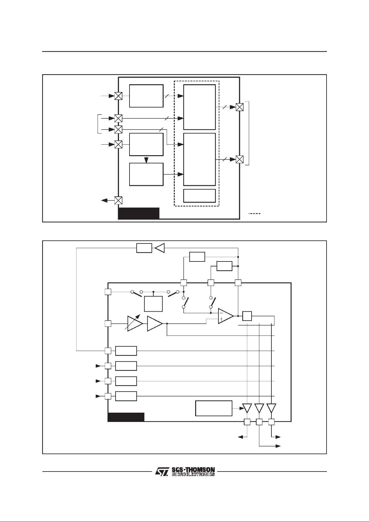
GENERAL BLOCKDIAGRAM
STV0056AF
From Tuner
Video
Processing
FromTV,
VCR/Decoder
FM
B-BAND
From Tuner
Demodulation
2 Channels
Wegener
Panda+
Deemphasis
22kHz to LNB
STV0056AF
VIDEOPROCESSINGBLOCK DIAGRAM
LPF
I/O/22kHz
B-BAND IN
25
22kHz
TONE
16
± 1
G
2
2
6x3
Video
4
Matrix
Audio
Matrix
+
Volume
2
I
C Bus
Interface
NTSC
PAL
VIDEEM1VIDEEM2/22kHz
9128
Baseband
3
3
To TV, VCR/Decoder
Active in Stand-by
UNCLDEEM
Deemphasized
÷ 2
0056F-02.EPS
CLAMPIN
S3 VID RTN
S2 VID RTN
S1 VID RTN
6
CLAMP
CLAMP
61
CLAMP
4
CLAMP
60
STV0056AF
Normal
DecoderReturn
VCRReturn
TV Return
BLACKLEVEL
ADJUST
63
64 2
To Decoder To VCR
S1 VID OUT
S2 VID OUTS3 VID OUT
To TV
0056F-03.EPS
7/27
Page 8
STV0056AF
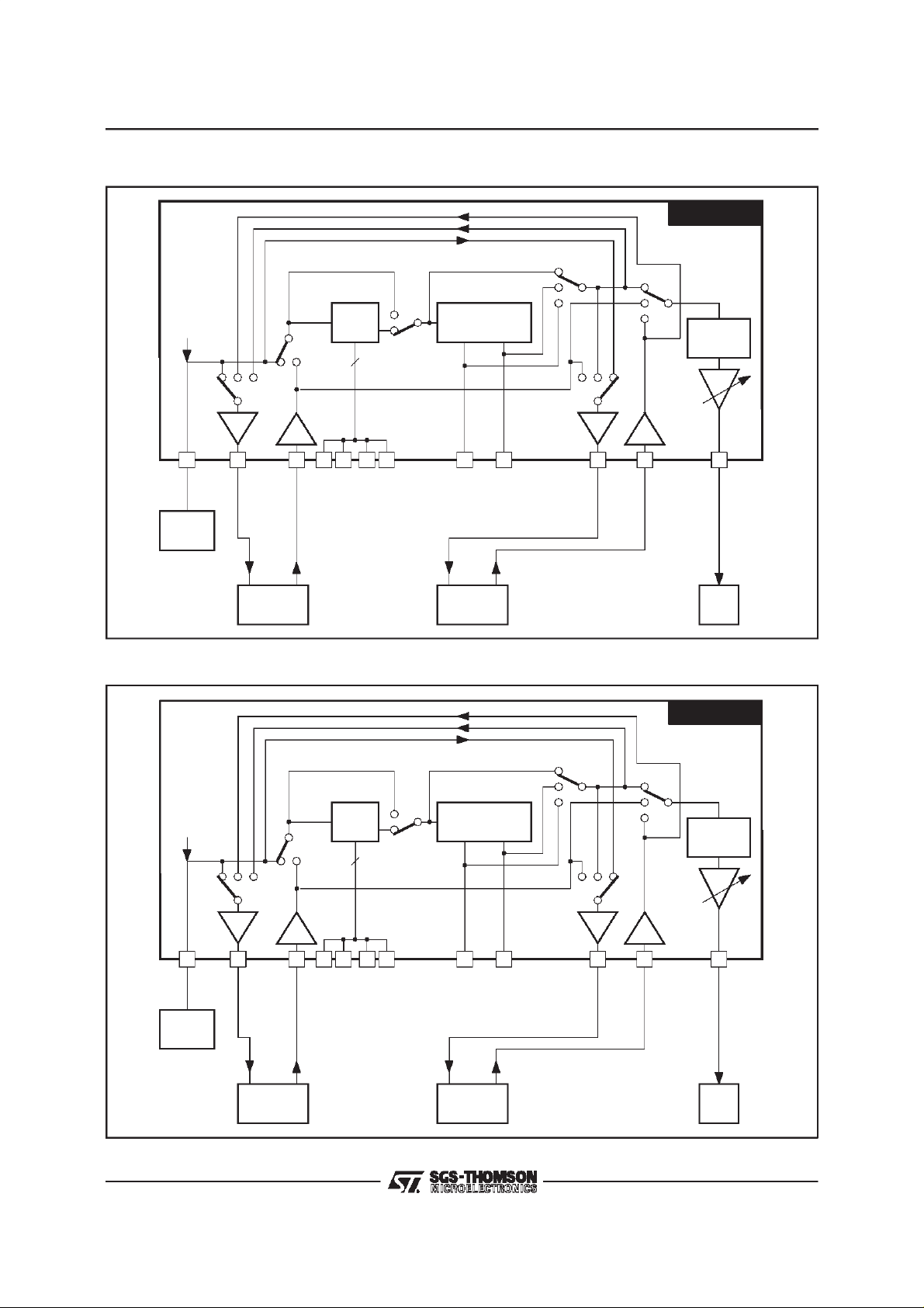
AUDIO PROCESSINGBLOCK DIAGRAM (CHANNELRIGHT)
AUDIO R
47
a
ANRS
K3
b
4
abc
K4
b
a
K6
-6dB -6dB
24 21 51 58 59 57 7 18 62
AUDIO
DEEMPHASIS
29 48
STV0056AF
K2
a
ba
c
abc
6dB6dB
K1
b
c
K5
MONO
STEREO
DET R
PLL
FILTER
Audio
Decoder Out
FC R
PK IN R
S3 OUT R
S3 RTN R
Audio
Decoder Return
LEVEL R
PK OUT R
J17 R
U75 R
DECODER VCR
AUDIO PROCESSINGBLOCK DIAGRAM(CHANNELLEFT)
AUDIOL
36
a
ANRS
K3
K4
abc
K6
23 20 52 54 53 55 5 17 3
b
a
-6dB -6dB
b
4
AUDIO
DEEMPHASIS
30 37
S2 OUT R
S2 RTN R
STV0056AF
K2
a
ba
c
abc
6dB6dB
K1
b
c
K5
MONO
STEREO
VOL R
TV
0056F-04.EPS
8/27
DET L
PLL
FILTER
Decoder Out
FC L
PK IN L
S3 OUT L
Audio
S3 RTN L
Audio
DecoderReturn
DECODER VCR
LEVEL L
PK OUT L
J17 L
U75 L
S2 OUT L
S2 RTN L
VOL L
TV
0056F-05.EPS
Page 9
AUDIO SWITCHING
STV0056AF
AUDIO
DEEMPHASIS
+ ANRS
AUDIOPLL
DECRTN
AUXIN K
K
1a
K
1b
1c 6b
VOL OUT AUXOUT
K
K
K
5b
5c
5a
FM DEMODULATION BLOCK DIAGRAM
FM IN
19
AGC
LEVEL
DETECTOR1
AGC R
39
LEVEL
DETECTOR2
K
K
K
DECOUT
Bias
6c
6a
SW1
0056F-06.EPS
Phase
Detect
:a→ANRS input non-scrambledaudio
K
4
b → ANRS input descrambledaudio
K
a
b
b
c
a
b
b
c
K
2
1
2
1
2
3
a
No ANRS, No De-emphasis
a
No ANRS, 50µs
a
No ANRS, 75µs
a
No ANRS, J17
b
ANRS, No De-emphasis
b
ANRS, 50µs
b
ANRS, 75µs
b
ANRS, J17
AUDIOR
FM dev.
Select.
V
REF
47
49
DET R
CPUMPR
AMPLKR
AGC L
AMPLK L
46
V
REF
AGC
22
38
V
REF
STV0056AF
Reg8 b4
LEVEL
DETECTOR1
LEVEL
DETECTOR2
Reg8 b0
Amp.Detect
WATCHDOG
SW3
Bias
Amp.Detect
WATCHDOG
Phase
Detect
90
VCO
0
SYNTHESIZER
AUDIOL
FM dev.
Select.
V
REF
90
VCO
0
SW2
SW4
36
35
DET L
CPUMP L
0056F-07.EPS
9/27
Page 10

STV0056AF
CIRCUITDESCRIPTION
VideoSection
Thecompositevideo is firstset to a standard level
by means of a 64 stepgain controlledamplifier. In
thecasethat themodulationisnegative,an inverter
canbe switched in.
One of two different external video de-emphasis
networks (for instance PALand NTSC) is selectable by an integrated bus controlledswitch.
Then energy dispersal is removed by a sync tip
clamping circuit, which is used on all inputs to a
video switching matrix, thus making sure that no
DC steps occur when switching videosources.
The matrix can be used to feedvideo to and from
decoders,VCR’sand TV’s.
A bus controlled black level adjustment circuit is
provided on the decoder output allowing a direct
connectionto an on-board Videocryptdecoder.
Additionaly all the video outputs are tristate type
(high impedance mode is supported), allowing a
simple parallel connections to the scarts (Twin
tunerapplications).
AudioSection
The two audio channels are totally independent
except for the possibility given to output on both
channelsonly one of theselectedinputaudiochannels.
To allow a very cost effective application, each
channel uses PLL demodulation.Neither external
complexfilter nor ceramic filtersare needed.
The frequency of the demodulated subcarrier is
chosenby a frequencysynthesizer which sets the
frequency of the internal local oscillator by comparing its phase with the internally generated
reference. When the frequency is reached, the
microprocessor switches in the PLL and the demodulationstarts.Atany momentthemicroprocessor can read from the device(watchdog registers)
the actual frequency to which the PLLis locked. It
canalsoverifythata carrierispresentatthewanted
frequency(by readingAMPLKstatusbit)thanks to
a synchronous amplitude detector, which is also
used forthe audio input AGC.
In order to maintain constant amplitude of the
recovered audio regardless of variations between
satellitesor subcarriers,the PLLloop gain may be
programmedfrom 56 values.
Any frequency deviation can be accomodated
(from ±30kHz till ±400kHz).
Two different networks can be permanently connectedfor either 75µsor J17de-emphasis.If 50µs
de-emphasisis required,thiscanbeinsertedby an
internal switch, thus allowinga worldwideapplication.
The STV0056AFis intendedto be compatiblewith
WegenerPanda System.
Twotypes of audio outputs are provided : oneis a
fixed 1V
2V
RMS
and the other is a gain controlled
RMS
max. The control range being from +12dB
to-26.75dBwith 1.25dBsteps.Thisoutputcanalso
be muted.
A matrixis implementedto feedaudio to and from
decodersVCR’s and TV’s.
Noise reduction system and de-emphasis can be
insertedor by-passed throughbus control.
Also all the audio outputs are tristate-type (high
impedancemode is supported),allowing a simple
parallelconnectionsto the scarts(Twintuner applications).
Others
A22kHz tone is generatedfor LNBcontrol.
It isselectableby buscontroland availableon one
of the two pins connected to the external video
de-emphasis networks. One general purpose I/O
is also available on the STV0056AF.
By means of the I
2
C bus there is the possibility to
drive the ICs into a low power consumption mode
with a ctive audio and video matrixes. Independantly from the main power mode, each individualaudioandvideooutputcanbedrivento high
impedancemode.
10/27
Page 11

STV0056AF
ABSOLUTEMAXIMUM RATINGS
Symbol Parameter Value Unit
V
CC
V
DD
P
tot
T
oper
T
stg
THERMAL DATA
Symbol Parameter Value Unit
Rth(j-a) Thermal Resistance Junction-ambient Max. 55
DC AND AC ELECTRICALCHARACTERISTICS
= 12V,VDD=5V,T
(V
CC
Symbol Parameter Test Conditions Min. Typ. Max. Unit
V
CC
V
DD
IQ
CC
IQ
DD
IQLP
CC
IQLP
DD
AUDIO DEMODULATOR
FMIN FM Subcarrier Input Level
DETH Detector 1 and 2 (AMPLOCK Pins)
VCOMI VCO Mini Frequency V
VCOMA VCO MaxiFrequency 10 MHz
AP50 1kHz AudioLevel at PLL output
APA50 1kHz Audio Level at PLL output
FMBW FM Demodulator Bandwidth Gain at 12kHz versus 1kHz
DPCO Digital Phase Comparator Output
AUTOMATIC NOISE REDUCTION SYSTEM
LRS Output Level (Pins LEVEL) 1V
LDOR Level Detector Output Resistance
NDFT Level Detector Fall Time Constant
NDLL Bias Level (PinsPK OUT) No audio in 2.40 V
LLCF NoiseReduction Cut-off Frequency at
HLCF Noise Reduction Cut-off Frequency at
Supply Voltage 15
7.0
Total Power Dissipation 900 mW
Operating Ambient Temperature 0, + 70
Storage Temperature -55, + 150
=25oC unless otherwise specified)
amb
Sypply Voltage 11.4
4.75125.0
Supply Current All audio and all video outputs
12.6
5.25VV
5587015mA
activated
Supply Current at Low Power Mode All audio and all video outputs
276359mA
are in high impedance mode
(Pin FMIN for AGC action)
VCO lockedon carrier at 6MHz
560kΩload onAMPLOCK Pins
5 500 mV
180kΩload onDET Pins
(Threshold for activating Level Detector 2)
(DET Pins)
(DET Pins)
8mV
Carrier without modulation
CC
T
amb
0.5V
Coarse deviation set to 50kHz
(Reg. 05 = 36
FMIN≤500mV
≤
PP
: 11.4 to 12.6V,
: 0 to 70oC
50kHz dev. FM input,
PP
)
HEX
PP
0.5VPP50kHz dev. FM input,
Coarse and fine settings used
2.90 3.10 3.30 V
5 MHz
0.6 1 1.35 V
0.92 1 1.08 V
0 0.3 1 dB
180kΩ, 82kΩ 22pF on DET Pins
Current (CPUMP Pins)
Average sink and source
current to external capacitor
on left and right channel 0.9 1 1.1 V
PP
60
4.0 5.4 6.8 kΩ
(Pins PK OUT)
(Pins PK OUT)
Low Level Audio
High Level Audio
External 22nF to GND and
1.2MΩto V
100mV
capacitor 330pF (FC Pins)
1V
PP
capacitor 330pF (FC Pins)
REF
on DET Pins, External
PP
on DET Pins, External
26.4 ms
0.85 kHz
7 kHz
o
V
V
o
C
o
C
C/W
mA
mA
PP
PP
A
µ
PP
0056F-03.TBL
0056F-04.TBL
PP
0056F-05.TBL
11/27
Page 12
STV0056AF
DC AND AC ELECTRICALCHARACTERISTICS(continued)
= 12V,VDD=5V,T
(V
CC
Symbol Parameter Test Conditions Min. Typ. Max. Unit
AUDIO OUTPUT (Pins VOL OUT R, VOL OUT L)
DCOL DC Output Level 4.8 V
AOLN Audio Output Level
with Reg 00= 1A
AOL50 AudioOutput Level
with Reg 00= 1A
AOL75 AudioOutput Level
with Reg 00= 1A
AOL17 AudioOutput Level
with Reg 00= 1A
AMA1 Audio Output Attenuation
with Mute-on. Reg 00 = 00.
MXAT Max Attenuation before Mute.
Reg 00 = 01.
MXAG Audio Gain. Reg 00 = 1F. 1kHz, from S2 RTN Pins 5 6 7 dB
ASTP Attenuationof each of the 31
steps
THDA1 THD with Reg 00 = 1A 1V
THDA2 THD with Reg 00 = 1A 2V
THDFM THD with Reg 00 = 1A FM input as for APA50
ACS Audio Channel Separation 1V
ACSFM Audio Channel Separationat 1kHz - 0.5 V
SNFM Signal to Noise Ratio FM input as for APA50,
SNFMNR Signal to Noise Ratio FM input as for APA50
Z
Z
OUT L
OUT H
Audio Output Impedance Low impedance mode
AUXILIARY AUDIO OUTPUT (PinsS2 OUT R, S2 OUT L, S3 OUT R, S3 OUT L)
DCOLAO DC output level Aux. input pins open circuit 4.8 V
AOLNS Audio Output Level
on S2 andS3
AOL50S Audio Output Level
on S2 andS3
AOL75S Audio Output Level
on S2 andS3
AOL17S Audio Output Level
on S2 andS3
AGAO S2 to S3Audio Gain
and S3to S2 AudioGain
THDA02 THD on S2, Input in S3 2V
=25oC unless otherwise specified)
amb
FM input as forAPA50
No de-emphasis, No pre-emphasis
No noise reduction
FM input as forAPA50
50µs de-emphasis, 27kΩ//2.7nF load
No pre-emphasis, No noise reduction
FM input as forAPA50
75µs de-emphasis, 27kΩ//2.7nF load
No pre-emphasis, No noise reduction
FM input as forAPA50
J17 de-emphasis, 36kΩ4.7kΩ8.2nF load
No pre-emphasis, No noise reduction
1VPP- 1kHz from S2 RTN Pins 60 65 dB
1kHz, from S2 RTN Pins 32.75 dB
1kHz 1.25 dB
-1kHz from S2 RTN Pins 0.15 %
PP
-1kHz from S2 RTN Pins 0.3 1 %
PP
75µs de-emphasis, ANRS ON
-1kHz on S2 RTN Pins 60 74 dB
PP
- 50kHz deviationFM input on
PP
one channel
- 0.5V
no deviation FM input on the
PP
other channel
- Reg 05 = 36
-75µs de-emphasis, no ANRS
75µs de-emphasis,
no ANRS, Unweighted
75µs de-emphasis,
ANRS ON, Unweighted
High impedance mode 301844 55ΩkΩ
FM input as forAPA50
No de-emphasis, No pre-emphasis
No noise reduction
FM input as forAPA50
50µs de-emphasis, 27kΩ//2.7nF load
No pre-emphasis, No noise reduction
FM input as forAPA50
75µs de-emphasis, 27kΩ//2.7nF load
No pre-emphasis, No noise reduction
FM input as forAPA50
J17 de-emphasis, 36kΩ4.7kΩ8.2nF load
No pre-emphasis, No noise reduction
1kHz -1 0 +1 dB
- 1kHz from Aux input pins 0.04 0.2 %
PP
1.5 1.9 2.34 V
2.0 3.3 4.0 V
2.0 3.3 4.0 V
2.0 3.2 4.0 V
0.3 1 %
60 dB
HEX
56 dB
69 dB
1.55 2 2.42 V
2.0 3.4 4.0 V
2.0 3.4 4.0 V
2.0 3.3 4.0 V
PP
PP
PP
PP
PP
PP
PP
PP
0056F-06.TBL
12/27
Page 13
STV0056AF
DC AND AC ELECTRICALCHARACTERISTICS(continued)
= 12V,VDD=5V,T
(V
CC
Symbol Parameter Test Conditions Min. Typ. Max. Unit
AUXILIARY AUDIO OUTPUT (PinsS2 OUT R, S2 OUT L, S3 OUT R, S3 OUT L) (continued)
THDAOFM THD on S2 or S3 FM input as for APA50
Z
OUT L
Z
OUT H
Audio Output Impedance Low impedance mode
I/O
V
V
V
V
LNB
LNB
IH
OL
OH
Low Level Input
IL
High Level Input 2.4
Low Level Output
High Level Output
Tone Frequency 22.2 22.2 22.2 kHz
T
Tone Signal Duty Cycle No load connected on I/O 49 50 51 %
D
RESET
RTCCU End of Reset Threshold for V
RTCCD Start of Reset Threshold for V
RTDDU End of Reset Threshold for V
RTDDD Start of Reset Threshold for V
COMPOSITE SIGNAL PROCESSING
VIDC VID IN Externalload current < 1µA 2.25 2.45 2.65 V
ZVI VID IN Input Impedance 7 11 14 k
DEODC DC Output Level (Pins VIDEEM) 2.25 2.45 2.65 V
DEOMX Max AC Level before Clipping
(Pins VIDEEM)
DGV Gain error vs GV @ 100kHz GV = 0 to 12.7dB, Reg 01 = 00→3F -0.5 0 0.5 dB
INVG Inverter Gain -0.9 -1 -1.1
VISOG Video Input to SCART Outputs
Gain
DEBW Bandwidth for 1V
measured on Pins VIDEEM
DFG Differential Gain on Sync Pulses
measured on Pins VIDEEM
ITMOD Intermodulation of FM subcar-
riers with chroma subcarrier
CLAMP STAGES (Pins CLAMP IN, S1, S2, S3 VID RTN)
ISKC Clamp Input Sink Current V
ISCC Clamp Input Source Current V
VIDEO MATRIX
XTK Output Level on any Output
when 1V
selected for any other output
PP
BFG OutputBufferGain(Pins S1VID
OUT,S2VIDOUT,S2 VIDOUT)
DCOLVH DC Output Level High impedance mode 0 0.2 V
Z
OUT HV
Video Output Impedance High impedance mode 16 23 30 k
VCL Sync Tip Level on Selected
Outputs (Pins S1 VID OUT, S2
VID OUT)
VCL S3 Sync Tip Level at S3 VID OUT
with Black Level Adjust
=25oC unless otherwise specified)
amb
75µs de-emphasis, no ANRS
High impedance mode 306044
I
= 2mA
sink
= 2mA 3.2
I
source
CCVDD
CCVDD
DDVCC
DDVCC
= 5V, VCCgoing up 8.7 V
= 5V, VCCgoing down 7.9 V
= 12V, VDDgoing up 3.8 V
= 12V, VDDgoing down 3.5 V
GV = 0dB, Reg 01 = 00 2 V
De-emphasis amplifier mounted in unity
gain, Normal video selected
PP
input
@ - 3dB with GV = 0dB, Reg 01 = 00 10 MHz
GV = 0dB, 1V
25Hz sawtooth (input : VID IN)
7.02 and 7.2MHz sub-carriers,
12.2dB lower thanchroma
= 3V 0.5 1 1.5
IN
=2V 40 50 60µA
IN
@ 5MHz TBD dB
CVBS input is
@ 100kHz 1.87 2 2.13
CVBS through 10nF on input 1.05 1.3 1.55 V
1V
PP
Register 4
b6 b7
00
01
10
11
CVBS + 0.5V
PP
PP
0.3 1 %
10055Ω
0.8 V
0.2
0.4 V
4.6
-1 0 1 dB
1%
-60 dB
1.36
1.52
1.67
1.84
k
Ω
V
V
Ω
PP
A
µ
Ω
V
V
V
V
0056F-07.TBL
13/27
Page 14

STV0056AF
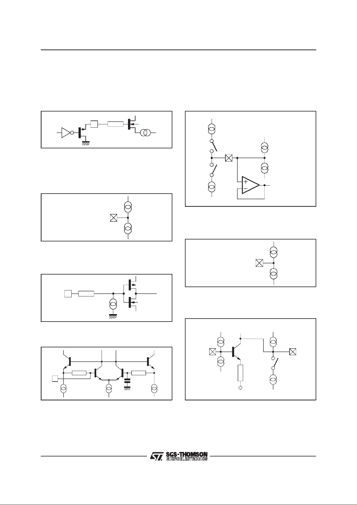
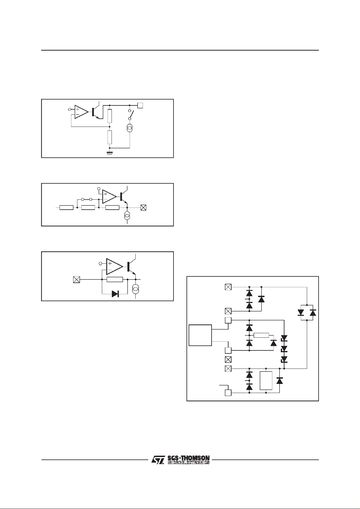
PIN INTERNALCIRCUITRY
S1 VID RTN, S2 VID RTN, S3 VID RTN,
CLAMPIN
50µAsourceis activeonly when VIDIN < 2.7V.
Figure 1
UNCLDEEM
Sameas above but with no black level adjustment
and slightly differentgain.
Figure 4
VDD9V
50µA
Pins60 - 4
61 - 6
10kΩ
S1 VID RTN
S2 VID RTN
S3 VID RTN
1µA
CLAMPIN
VDD5V
GND0V
S3 VID OUT
Iblacklevelis I2Cprogrammablefromsource16µA
to sink 33µA equivalent to an offset voltage of
-150mVto + 300mV. The 60Ω collector resistor is
for short cct. protection.
Figure2
VID MUX
60Ω
4
2.3mA
GND 0V
V
CC
10kΩ
16.7kΩ
GND 0V
12V
S3 VID OUT
63
25kΩ
I Black Level
V
2.4V
REF
S1 VID OUT, S2 VID OUT
Sameas abovebut with no blackleveladjustment.
Figure3
60
Ω
12V
V
CC
60Ω
VCC12V
4
2.3mA
0056F-08.EPS
VIDEEM1
IN
GND 0V
10kΩ
16.7kΩ
Ron of the transistor gate is ≈10kΩ.
Figure 5
6µ/2µ
10µ/2µ
VIDEEM1
12
VIDEEM2/ 22kHz
Ron of the transistor gate is ≈10kΩ.
Figure 6
6µ/2µ
10µ/2µ
VIDEEM2/22kHz
0056F-09.EPS
9
100µ/2µ
60µ/2µ
25kΩ
UNCLDEEM
8
V
2.4V
REF
GND0V
0056F-11.EPS
125µA
0056F-12.EPS
125µA
5V
V
DD
22kHz
0056F-13.EPS
VIDMUX
14/27
4
2.3mA
GND 0V
10k
Ω
20k
Ω
20kΩ
GND 0V
Pins 64 - 2
S1 VID OUT
S2 VID OUT
V
2.4V
REF
VID IN
Figure 7
0056F-10.EPS
B-BAND
V
2.4V
REF
10kΩ
6.5kΩ
16
IN
0.5pF
GND 0V
85µA
0056F-14.EPS
Page 15

PIN INTERNALCIRCUITRY(continued)
PK OUT R, PK OUT L
Figure8
3.4V
VDD9V
Audio
1
1
Peak Detector
5k
Clamp
Ω
Pins 51 - 52
PK OUT R
PK OUT L
FC L, FC R
Ivar is controlled by the peak det audio level max.
±15µA(1V
PP
audio).
Figure9
V
9V
Pin 55 - 57
FC L - FC R
1
DD
1
Ivar
VOL OUT R, VOL OUT L
Audio output with volume and scart driver with
+12dB of gain for up to 2V
. The opamp has a
RMS
push-pulloutputstage.
Figure10
Audio
2.4VBias
30kΩ
30kΩ
4.8V
GND0V
15kΩ
Pins 62 - 3
VOL OUTR
VOL OUTL
S2 OUT L, S2 OUT R, S3 OUT L, S3 OUT R
Sameas above but with gain fixed at +6dB.
Figure11
Audio
2.4V Bias
20kΩ
20k
Ω
Pins 5 - 7 - 23 - 24
S2 OUT L
S2 OUT R
S3 OUT L
S3 OUT R
GND 0V
STV0056AF
S2 RTN L, S2 RTN R, S3 RTN L, S3 RTN R
4.8V bias voltageis the same as the biaslevel on
the audio outputs.
Figure 12
4.8V
Pins 17 - 18 - 20 - 21
S2 RTN L - S2 RTN R
S3 RTN L - S3 RTN R
0056F-15.EPS
FM IN
Theotherinputforeachchannelisinternallybiased
in the same way via 10kΩ to the 2.4V V
Figure 13
2.4V
FM IN
19
I
REF
0056F-16.EPS
The optimum value if I
10k
Ω
10kΩ
Right Channel
external resistorof 47.5kΩ ±1% is required.
Figure 14
2.4V
I/O / 22kHz
The input is TTL compatible.
The output is tri-stateable.
Figure 15
0056F-17.EPS
MUX
22kHz
180µ/2µ
100µ/2µ
I/O/22kHz
SCL
Thisis theinput toa Schmittinputbuffer madewith
a CMOSamplifier.
Figure 16
SCL 24µ/4µ
0056F-18.EPS
205Ω
26
ESD
25kΩ
Left Channel
50µA
50µA
is 50µA ±2% so an
REF
1
I
50
REF
205
25
Ω
ESD
REF
50µA
0056F-19.EPS
.
0056F-20.EPS
0056F-21.EPS
10µ/2µ
IIC Reg
91µ/2µ
0056F-22.EPS
0056F-23.EPS
15/27
Page 16
STV0056AF
PIN INTERNALCIRCUITRY(continued)
SDA
Inputsame as above.
Output pull down only : relies on external resistor
for pull-up.
Figure17
CPUMP L, CPUMP R
An offset on the PLL loop filterwill cause an offset
in the two 1µA currents that will prevent the PLL
from drifting-offfrequency.
Figure 21
SDA
600µ/2µ
27
GND 0V
205
ESD
Ω
24µ/4µ
J17 L, J17 R, U75 L, U75 R
I1 - I2 = 2 x audio/ 18kΩ.eg1VPPaudio: ±55µA.
The are internal switches to matchthe audio level
of the different standards.
Figure18
Pins 30 - 29
37 - 48
J17 L - J17 R
U75 L - U75R
I1
I2
HA
Inputwith CMOSlevels.
Figure19
25µ/2µ
10µ/2µ
HA
28
205
ESD
Ω
150µA
GND 0V
100µA
Pins 35-49
0056F-24.EPS
Dig Synth
CPUMP L
CPUMP R
100µA
1µA
LoopFilter Tracking
1µA
VCO Input
DET L, DET R
I2 - I1 = f (phase error).
Figure 22
0056F-25.EPS
I2
Pins 36 - 47
DET L - DET R
I1
AMPLK L, AMPLK R, AGC L, AGC R
I2 and I1 fromthe amplitude detectingmixer.
Figure 23
0056F-26.EPS
0056F-28.EPS
0056F-29.EPS
XTL
Figure20
XTL
31
16/27
460Ω
750µA
232
To VCA
Pin 38
Pin 46
AMPLKL
AMPLKR
460Ω
5pF
GND 0V
500µA
3
750µA
0056F-27.EPS
I2
2
I1
Ω
10k
V
2.4V
REF
5µA
160µA
Pin 22
Pin 39
AGC L
AGC R
0056F-30.EPS
Page 17
PIN INTERNALCIRCUITRY(continued)
V
REF
The400µA sourceis offduring stand-bymode.
Figure24
V
(2.4V)
43
Vbg 1.2V
4
10kΩ
10kΩ
GND0V
REF
400µA
STV0056AF
VDD5V, GND 5V
Connected to XTL oscillator and the bulk of the
CMOS logic and 5V ESD.
A GND
Doubledbonded :
- One pad connected to the left VCO, dividers,
mixers and guard ring. the guard connection is
star connecteddirectlyto the pad.
- The secondpadis connectedto both AGCamps
and the deemphasis amplifiers, frequency synthesis and FM deviation selection circuitfor both
0056F-31.EPS
channels.
LEVELL, LEVELR
Figure25
V
2.4V
REF
Audio
SW
49kΩ49kΩ
50kΩ
1
100µA
Pins 59 - 53
LEVEL R
LEVEL L
PK IN L, PK IN R
Figure26
V
2.4V
REF
Pins 58 - 54
PK IN R
PK IN L
67kΩ
1
To Peak Det
100µA
V 12V
Doubledbonded (twobond wiresand two padsfor
one package pin) :
- One pad is connected to all of the 12V ESD and
video guard rings.
- The second pad is connected to power up the
video block.
V GND
Doubledbonded:
- Onepadisconnectedto power-upallofthevideo
mux and I/O.
- The second pad is only as a low noise GND for
the video input.
A 12V
Doubledbonded :
- One pad connected to the ESD and guard ring.
- The second pad is connectedto the main power
for all of the audio parts.
A GND R
Boubled bonded :
- One pad connected to the right VCO, dividers,
0056F-32.EPS
mixers and guard ring. The guard connection is
star connecteddirectlyto the pad.
- The second pad is connected to the bias block,
audio noisereduction,volume, mux and ESD.
A third bond wire on this pin is connected directly
to the die pad (substrate).
Figure 27
Pins 10 - 11
V 12V
V GND
V
DD
GND 5V
A GND L
A 12V
A GND R
Video Pads
32
5V
Digital Pads
33
Audio Pads
56
205Ω
BIP
12V
DZPN1
DZPN1
DZPN1
+
-
0056F-33.EPS
Pins 13 - 14
Vpp
BIP 10vpl
Vmm
Pins 41 - 42
Substrate
0056F-34.EPS
17/27
Page 18

STV0056AF
I2C PROTOCOL
1) WRITING to the chip
S-StartCondition
P-Stop Condition
CHIPADDR -7 bits. Programmable06H or 46H (STV0056AFonly) with Pin HA.
W-Write/Read bit is the 8th bit of the chip address.
A-ACKNOWLEDGEafter receiving 8 bits of data/adress.
REGADDR
DATA 8 bits ofdatabeing written to theregister.All8 bitsmustbewrittentoatthesame
REGADDR/A/DATA/A can be repeated,the write process can continue untill terminated with a STOP
Example:
S06WA00A55A01A8F A P
Address of register to be written to, 8 bits of which bits 3, 4, 5, 6 & 7 are ’X’ or
don’t care ie
only the first 3 bitsare used
.
time.
condition.If the
REG ADDR
is higher than 07 then IIC PROTOCOL will still be
met (ie an A generated).
2) READING
from thechip
Whenreading,thereis an auto-incrementfeature.Thismeans anyreadcommandalwaysstartsbyreading
Reg 8 and will continue to read the following registers in order after each acknowledge or until there is no
acknowledge or a stop. This function is cyclic that is it will read the same set of registers without
re-addressingthe chip. There are two modes of operationas set by writing to bit 7 of register 0. Read 3
registersin a cyclic fashion or all 5 registersin a cyclic fashion. Noteonly thelast 5 of the11registerscan
be read.
Reg0 bit 7 = L ⇒ Start/ chip add / R /A/ Reg8 / A/ Reg9 / A/ Reg 0A/ A/ Reg8 / A/ Reg 9 / A/ Reg 0A
/... / P /
Reg0 bit 7 = H⇒ Start/ chip add / R / A / Reg 8 / A/ Reg 9 / A/ Reg 0A/ A/ Reg 7 / A/ Reg 6 / A/ Reg 8
/ A/ Reg 9 / A / Reg 0A / A/ Reg 7 / A / Reg 6 / ... / P /
CONTROL REGISTERS
Reg 0 writeonly
Bit (default 00
HEX
)
0 L Select 5 bitsaudio volume control 00H = MUTE
1 L Select 5 bitsaudio volume control 01H = -26.75dB
2 L Select 5 bitsaudio volume control : : : : :
3 L Select 5 bitsaudio volume control 1.25dB steps up to
4 L Select 5 bitsaudio volume control 1FH = +12dB
5 L Audio mux switch K4 - ANRSI/P select (L= PLL)
6 L Audio mux switch K3 - ANRSselect(L = no ANRS, H = ANRS)
7 L L = read3 registers,H = read 5 registers
Reg 1 writeonly
Bit (default 00
HEX
)
0 L Select video gain bits
1 L Select video gain bits 00H = 0dB
2 L Select video gain bits 01H = +0.202dB
3 L Select video gain bits 02H = +0.404dB
4 L Select video gain bits n = + 0.202 dB * n
5 L Select video gain bits 3FH = + 12.73 dB
6 L Selectedvideo invert (H = inverted, L= non inverted)
7 L Videodeemphasis 1 / Videodeemphasis2 (L : V
18/27
De-em1)
ID
Page 19

CONTROL REGISTERS (continued)
Reg 2 writeonly
Bit (default F7
HEX
)
0 H Select video source for scart1 O/P
1 H Select video source for scart1 O/P
2 H Select video source for scart1 O/P
3 L Select 4.000MHzor 8.000MHzclock speed (L = 8MHz)
4 H Select audio source for volume output (Switch K1)
5 H Select audio source for volume output (Switch K1)
6 H Select Left/Right/Stereofor volume output
7 H Select Left/Right/Stereofor volume output
Reg 3 writeonly
Bit (default F7
HEX
)
0 H Select video source for scart2 O/P
1 H Select video source for scart2 O/P
2 H Select video source for scart2 O/P
3 L Videodeemphais 2 / 22kHz(H : 22kHz)
4 H Select audio source for Scart 2 output (Switch K5)
5 H Select audio source for Scart 2 output (Switch K5)
6 H Audio deemphasisselect(Switch K2)
7 H Audio deemphasisselect(Switch K2)
STV0056AF
Reg 4 writeonly
Bit (default BF
HEX
)
0 H Select source for video decoder O/P
1 H Select source for video decoder O/P
2 H Select source for video decoder O/P
3 H Stand-byor lowpower mode (H = low power)
4 H Select audio source for Scart 3 output (Switch K6)
5 H Select audio source for Scart 3 output (Switch K6)
6 L Black level adjust on Scart3 video
7 H Black leveladjust on Scart3 video
Reg 5 writeonly
Bit (default B5
HEX
)
0 H FM deviationselection-- default value for 50kHzmodulation
1 L FM deviationselection
2 H FM deviationselection
3 L FM deviationselection
4 H FM deviationselection
5 H FM deviationselection(L = double the FM deviation)
6 L Select 22kHz for I/O (Pin29 / STV0056AF)
7 H Select TP50a (H) or I/O (Pin 29 / STV0056AF).TP50a for testonly.
Reg 6 write/read
Bit (default 86
HEX
)
0 L Statusof I/O
1 H Select data direction of I/O1 ( H = output)
2 H Select frequencysynthesizer1 OFF/ON(L = OFF)
3 L Select frequencysynthesizer2 OFF/ON(L = OFF)
4 L Select RF source (L = OFF) to FM det 1
5 L Select RF source (L = OFF) to FM det 2
6 L Select frequencyfor PLL synthesizer- LSB (bit 0) of 10-bit value
7 H Select frequencyfor PLL synthesizer- bit 1 of 10-bit value
19/27
Page 20

STV0056AF
CONTROL REGISTERS (continued)
Reg 7 write/read
Bit (defaultAF
0 H Select frequencyfor PLL synthesizer- bit 2 of 10-bit value
1 H Select frequencyfor PLL synthesizer
2 H Select frequencyfor PLL synthesizer
3 H Select frequencyfor PLL synthesizer
4 L Select frequencyfor PLL synthesizer
5 H Select frequencyfor PLL synthesizer
6 L Select frequencyfor PLL synthesizer
7 H Select frequencyfor PLL synthesizer- bit 9, MSB(10th bit) of 10-bit value
Reg 8 readonly
Bit
0 Subcarrierdetection(DET 1) (L = No subcarrier)
1 Not used
2 Read frequencyof watchdog1 - LSB (bit0) of 10-bitvalue
3 Read frequencyof watchdog1 - bit 1 of 10-bit value
4 Subcarrierdetection(DET 2) (L = No subcarrier)
5 Not used
6 Read frequencyof watchdog2 - bit 0 of 10-bit value
7 Read frequencyof watchdog2 - bit 1 of 10-bit value
HEX
)
Reg 9 readonly
Bit (defaultAF
HEX
)
0 Read frequencyof watchdog1 - bit 2 of 10-bit value
1 Read frequencyof watchdog1
2 Read frequencyof watchdog1
3 Read frequencyof watchdog1
4 Read frequencyof watchdog1
5 Read frequencyof watchdog1
6 Read frequencyof watchdog1
7 Read frequencyof watchdog1 - bit 9, MSB (10th bit) of 10-bit
Reg 0A read only
Bit
0 Read frequencyof watchdog2 - bit 2 of 10-bit value
1 Read frequencyof watchdog2
2 Read frequencyof watchdog2
3 Read frequencyof watchdog2
4 Read frequencyof watchdog2
5 Read frequencyof watchdog2
6 Read frequencyof watchdog2
7 Read frequencyof watchdog2 - bit 9, MSB (10th bit) of 10-bit
20/27
Page 21

CONTROL REGISTERS (continued)
VideoMux Truth Tables
Register2 <0:2>⇒ Scart 1 video outputcontrol
Register3 <0:2>⇒ Scart 2 video outputcontrol
Register4 <0:2>⇒ Scart 3 decoderoutput control
Thetruth table for the three scart outputsare the same.
Register 2/3/4 Video Output
Bit<2>
0
0
0
0
1
1
1
1
Bit <7>
Bit<1>
0
0
1
1
0
0
1
1
Register 4 Black Level Adjust on Scart 3
0
1
0
1
Bit<0>
Bit <6>
0
0
1
1
0
Baseband video
1
De-emphasized video
0
Normal video
1
Scart 3 return
0
Scart 2 return
1
Scart 1 return
0
Nothing selected
1
High Z or low power (default)
-150mV
0 (default)
+150mV
+300mV
STV0056AF
AudioMux Truth Tables
Register 2 Switch K1/Audio Source Selection for Volume Output
Bit <5>
0
1
0
1
Bit <7>
0
1
0
1
Bit <6>
0
1
X
X
Bit <5>
0
1
0
1
Bit <4>
0
0
1
1
Register 3 Switch K2/Audio Deemphasis
Bit <6>
0
0
1
1
Register 0 Switch K3 & K4
Bit <5>
X
X
0
1
Register 3 Switch K5/Audio Source Selection for Scart 2
Bit <4>
0
0
1
1
Volume Output
A
Audio deemphasis (K2 switch O/P)
C
Scart 2 return
B
Scart 3 return
-
High Z or low power (default)
Audio Deemphasis
A
No deemphasis
C
J17
B
50µs
B
75µs (default)
ANRS I/O Select
A
Noise reduction OFF
B
Noise reduction ON (default)
A
I/P = PLL
B
I/P = Scart 3 return
Aux Audio Output
C
PLL output
A
Scart 3 return
B
Audio deemphasis (K2 switch O/P)
-
High Z or low power state (default)
Bit <5>
0
1
0
1
Register 4 Switch K6/Audio Source Selection for Scart 3
Bit <4>
0
0
1
1
Audio Decoder Output
A
PLL output
C
Audio deemphasis (K2 switch O/P)
B
Scart 2 return
-
High Z or low power state (default)
21/27
Page 22

STV0056AF
CONTROL REGISTERS (continued)
Register 2 Left / Right / Stereo on Volume Output
Bit <7>
0
1
1
Register5 : FM DeviationSelection
43210
0
0
0
0
0
0
0
0
0
0
0
0
0
0
0
0
1
1
1
1
1
1
1
1
1
1
1
1
1
1
1
1
Example : Default power up state54.4kHz ⇒±54.4kHz.
0
0
0
0
0
0
0
0
1
1
1
1
1
1
1
1
0
0
0
0
0
0
0
0
1
1
1
1
1
1
1
1
Bit <6>
0
0
1
0
0
0
0
1
1
1
1
0
0
0
0
1
1
1
1
0
0
0
0
1
1
1
1
0
0
0
0
1
1
1
1
Mono left /channel 1
Mono right / channel 2
Stereo left & right (default)
0
0
1
1
0
0
1
1
0
0
1
1
0
0
1
1
0
0
1
1
0
0
1
1
0
0
1
1
0
0
1
1
0
1
0
1
0
1
0
1
0
1
0
1
0
1
0
1
0
1
0
1
0
1
0
1
0
1
0
1
0
1
0
1
Selected Nominal Carrier Modulation
Bit 5 = 0 Bit 5 = 1
Do not use
Do not use
Do not use
Cal. set. (2V)
592kHz
534kHz
484kHz
436kHz
396kHz
358kHz
322kHz
292kHz
266kHz
240kHz
218kHz
196kHz
179kHz
161kHz
146kHz
122kHz
120kHz
109kHz
98kHz
89kHz
78kHz
71kHz
65kHz
58kHz
53kHz
48.6kHz
43.8kHz
39.6kHz
cal : do not use = 0.3373V offset on VCO
cal : do not use = 0.3053V offset on VCO
cal : do not use = 0.2763V offset on VCO
calibration setting (1V offset on VCO)
296kHz modulation
267kHz modulation
242kHz
218kHz
198kHz
179kHz
161kHz
146kHz
133kHz
120kHz
109kHz
98.3kHz
89.7kHz
80.9kHz
73.1kHz
66.0kHz
60.0kHz
54.4kHz = default power up state
49.1kHz
44.3kHz
39.8kHz
35.9kHz
32.4kHz
29.1kHz
26.7kHz
24.3kHz
21.9kHz
19.7kHz
Register 1
Bit <7>
Bit <7>
22/27
Register 3
Bit <3>
0
0
1
1
Register 5 Digital I/O (STV0056AF pin 29)
0
0
1
1
0
1
0
1
Bit <6>
0
1
0
1
Deemphasis 1 (default)
Deemphasis 1 + 22kHz
Deemphasis 2
Deemphasis 2
I/O (refer to Register 6 Bit <0> Bit <1>)
22kHz
Do not use (for test only) (default)
22kHz
Video Deemphasis/22kHz
Page 23

FMDEMODULATION SOFTWAREROUTINE
WiththeSTV0056AFcircuit,foreachchannel,three
stepsare requiredto acheivea FM demodulation:
st
step:To set the demodulationparameters :
-1
• FM deviationselection,
• Subcarrier frequencyselection.
nd
-2
step : To implement a waitingloop to check
the actual VCOfrequency.
rd
step:To closethedemodulationphaselocked
-3
loop (PLL).
Refering to the FM demodulation block diagram
(page 12), the frequencysynthesis block is commonto bothchannels(leftand right);consequently
twocompletesequenceshaveto bedoneoneafter
the other when demodulatingstereo pairs.
Detailed Description
Conventions:
- R = Stands for Register
- B = Stands for Bit
Example :
R05 B2 = Register05, Bit 2
For clarity, the explanationsare based on the following example : stereo pair 7.02MHz/L
7.20MHz/R,deviation±50kHz max.
1stSTEP (LEFT) : SETTINGTHE DEMODULATIONPARAMETERS
A. The FM deviationis selected by loadingR5 with
the appropriate value. (see R5 truth table).
TheTable1 givesthesettingforthemostcommon
subcarrierfrequencies.
NB : Verywide deviations(up to ±592kHz)can be
accomodatedwhen R5 B5is low.
Corresponding bandwidth can be calculated as
follows:
Bw ≈ 2 (FMdeviation + audio bandwidth)
Bw ≈ 2 (valuegiven in table+ audio bandwidth)
In the example :
R5Bits 76543210
XX110110
B.
The subcarrier frequency is selected by
launchingafrequencysynthesis(theVCOisdriven
to the wanted frequency).This operationrequires
twoactions :
- To connect the VCO to the frequency synthesis
loop.ReferingtotheFMblockdiagram(page 12):
• SW4 closed ⇒ R6 B2 = H
• SW3 to bias ⇒ R6 B4 = L
• SW2 to bias
⇒ R6 B3 = L
• SW1 opened ⇒ R6B5 = L
- To load R7 and R6 B6 B7 with the value corre-
sponding to the left channel frequency. This 10
bits value is calculated as follows:
Subcarrierfrequency = coded value x 10kHz
(10kHz is the minimum step of the frequency
synthesis function)
Considering that the tunning range is comprised
between5 to10MHz,thecoded valueis anumber
between 500 and 1000 (2
10
= 1024)then 10 bits
are required.
Example :
7.02MHz= 702x 10kHz
702 ⇒ 1010 1111 10 ⇒ AF + 10
R7 is loaded with AF and R6 B6 : L, R6 B7 : H.
Table 1 : FrequencySynthesisRegisterSetting
for the Most Common Subcarrier Frequencies
Subcarrier Frequency
(MHz)
5.58 8B 1 0
5.76 90 0 0
5.8 91 0 0
5.94 94 1 0
6.2 9B 0 0
6.3 9D 1 0
6.4 A0 0 0
6.48 A2 0 0
6.5 A2 1 0
6.6 A5 0 0
6.65 A6 0 1
6.8 AA 0 0
6.85 AB 0 1
7.02 AF 1 0
7.20 B4 0 0
7.25 B5 0 1
7.38 B8 1 0
7.56 BD 0 0
7.74 C1 1 0
7.85 C4 0 1
7.92 C6 0 0
8.2 CD 0 0
8.65 D8 0 1
Register 7
(Hex)
STV0056AF
Register 6
Bit7 Bit6
23/27
Page 24

STV0056AF
FMDEMODULATION SOFTWAREROUTINE (continued)
2ndSTEP (LEFT) :
VCO FREQUENCY CHECKING(VCO)
Thissecondstepis actuallya waitingloop in which
the actual running frequencyof the VCO is measured.
To exit of this loop is allowed when : Subcarrier
Frequency- 10kHz ≤ MeasuredFrequency≤ Subcarrier Frequency + 10kHz (± 10kHz is the maximum dispersion of the f requency synthesis
function).
In practice, R8 B2 B3 and R9 are read and compared to the value loaded in R6 B6 B7 and R7
±1 bit.
Note :
The duration of this step depends on how large is
frequencydifference between the start frequency
and the targeted frequency. Typically :
- therate ofchangeof the VCO frequencyis about
3.75MHz/s(C
pump
=10µF)
- In addition to this settling time, 100ms must be
added to takeintoaccountthesamplingperiodof
the watchdog.
3rdSTEP (LEFT)
TheFMdemodulationcan be startedbyconnecting
the VCO to the phase locked loop (PLL).
In practice:
- SW3 closed ⇒ R6 B4 = H
- SW4 opened ⇒ R6 B2 = L
After this sequence of 3 steps for left channel,
a similarsequenceis neededfor the rightchannel.
Note :
In the sequence for the right, there is no need to
again select the FM deviation (onceis enough for
the pair).
GeneralRemark
Before to enable the demodulated signal to the
audiooutput, it is recommandedto keepthemuting
and to checkwhethera subcarrieris presentat the
wantedfrequency.Suchan informationis available
in R8 B0 and R8 B4which can be read.
Twodifferentstrategiescanbeadoptedwhen enabling the output:
- Eitherboth left and rightdemodulatedsignalsare
simultaneously authorized when both channel
are ready.
- Orwhile therightchannelsequenceisrunning,the
alreadyreadyleft signalis senttotheleftandright
outputs and the real stereo sound L/R is output
whenbothchannelsareready.Thissecondoption
givessounda few hundredsof ms beforethe first
one.
24/27
Page 25
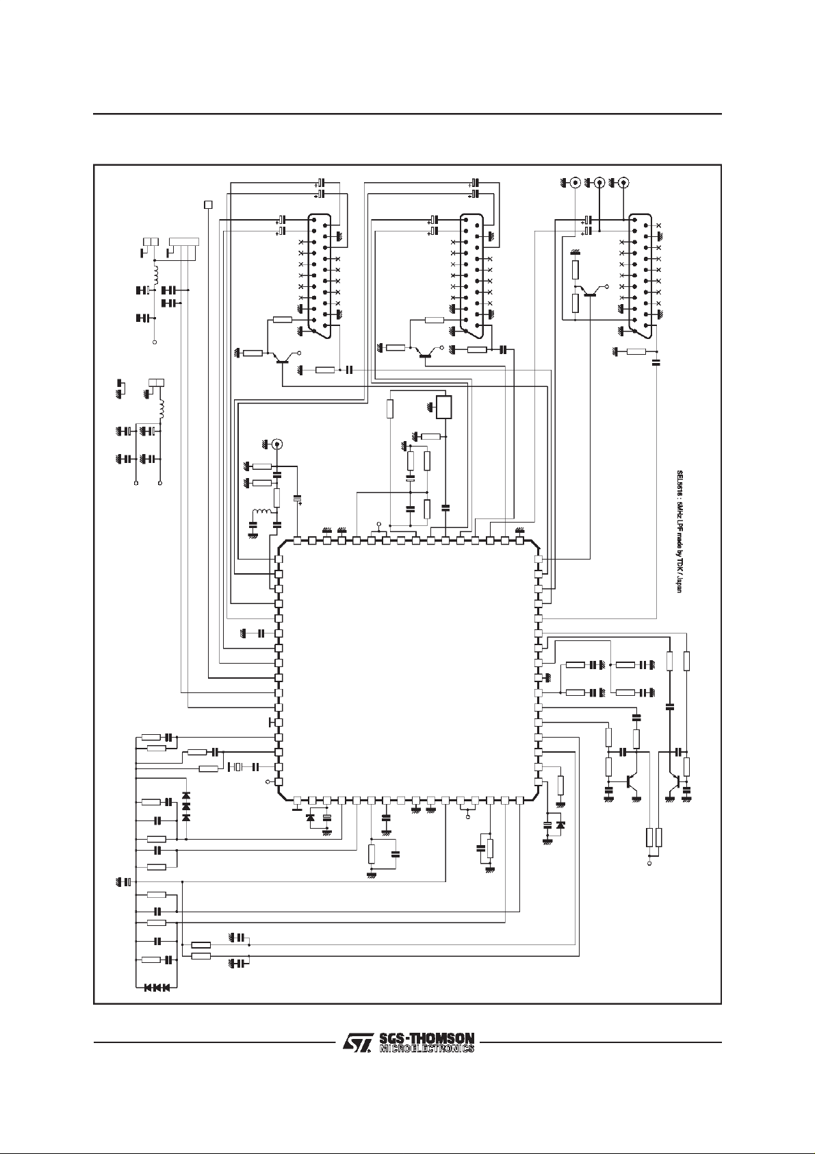
TYPICALAPPLICATION (3 SCARTS, PAL/SECAMEurope Apllication)
C5 2.2µF
R568
Q2
R16
1k
Ω
R10 10kΩ
Ω
V
CCV
SEL5618
1
2
3
C11 8.2nF
674
C7 2.2µF
C8 2.2µF
1
3
5
7
9
11
13
15
17
19
21 J2
R6 75Ω
TDK FILTER
5
2
4
6
8
VCR SCART
10
12
14
16
18
20
220nF
C4
2
3
16V
220µF
100nF
C103 2.2µF
J8
1I/O
GND
GND
SDA
SCL
J12
16V
1
220µF
C30
100nF
J14
L1 22µH
+
C31
GND
1
5V
J11
47pF
47pF
J10
123
4
C65
C66
15V
V
DD
R101 470Ω
J13
112V
L2 22µH
+
+
C35
C33
220µF
16V
C34
C32
100nF
V
V
CCV
CCA
C24 27pF
75
R48
Ω
R18
1k
Ω
L4
47µH
C105 2.2µF
C102 2.2µF
R10368Ω
BC547
Q101
TUNER
INPUT
J7
100pF
R17 470Ω
8.2nF
C25
C23
CCV
16
C104 2.2µF
1
2
3
4
5
6
7
8
9
10
11
12
13
14
15
16
17
18
19
20
21 J3
V
R102 75Ω
10µF 16V
C26
15
C6 2.2µF
DECODERSCART
220nF
C101
BC547
R4 470Ω
R15 1kΩ
R11 1.5kΩ
10µF 16V
C13
+
C12100pF
R9 5.1kΩ
V
CCV
11
12
13
14
10
8
9
17 18 19 20
STV0056AF
J6
J5
J4
R
L
V
2.2µF
C3
C2
2.2µF
R3 470Ω
BC547
Q1
R268Ω
1
V
CCV
1
3
5
7
9
11
13
15
17
19
21 J1
R100 75Ω
2
4
6
8
TV SCART
10
12
14
16
18
20
220nF
C100
21
22 23 24 25 26 27 28
C56 100nF
4.7k
8.2nF
R104
C107
Ω
R105 36kΩ
82k
R32
Ω
C38 22pF
22pF
C37
R107 4.7kΩ
C108 8.2nF
3 x 1N4148
8MHzCrystal
R106
36k
Ω
3029
C29
22pF
4MHzor
32313029
V
DD
35
34
33
C41
8.2V
38
37
36
10µF 16V
+
R33 180kΩ
560kΩ
C39 2.7nF
R34 27kΩ
+
C40
470µF
16V
R39 27kΩ
TQFP64
4041424344
39
100nF
C43
100nF
R36
C42
STV0056AF
45
V
CCA
100nF
C45
100nF
1.2M
C66
R60
Ω
5758596061626364
5056 55 54 53 52 51
49
47
48
46
10µF 16V
C50
1.5nF
43k
C60
R53
Ω
3.3k
Ω
1.5k
R50
8.2V
Ω
1.5nF
47.5kΩ 1%
+
R114
R115
C113
8.2nF
43k
Ω
1.2M
Ω
C114
1.5nF
C64
R58
100nF
C65
R59
R54 3.3kΩ
R57 24kΩ
C63 220nF
220nF
C115
R117
24k
8.2nF
C62
Ω
1.5k
R55
Ω
BC557
BC557
Q103
Q4
1.5nF
C61
R116 10kΩ
R56 10kΩ
R37 560kΩ
V
CCA
C46 2.7nF
R40 180kΩ
R51 560kΩ
C58 100nF
C47 22pF
C48
22pF
R41
82k
R113 560kΩ
Ω
3 x 1N4148
C112 100nF
0056F-35.EPS
25/27
Page 26

STV0056AF
TWINTUNER APPLICATION
Easyparallel connectionof the outputsto the scarts without any additional switchinghardware.
This configuration is possible due to the high impedance mode that can be selected for each audio and
video outputs.
2
I
C Bus
TUNER1
TUNER2
5V
28
28
64
S
T
V
A
2
0
63
0
5
6
62-3
5-7
23-24
F
64
S
T
V
A
2
0
63
0
5
6
62-3
5-7
23-24
Video
TV
SCART
Audio
2
Video
VCR
SCART
Audio
2
Video
DECODER
SCART
Audio
2
F
0056F-36.EPS
26/27
Page 27

PACKAGE MECHANICAL DATA
64 PINS - PLASTICQUAD FLATPACK (THIN) (TQFP)
D
D1
49
3348
32
0.10mm
Seating Plane
STV0056AF
A
A2
A1
B
C
Dimensions
B
64
1
e
TQFP6 4
E3D3E1
17
16
E
L1
L
K
Millimeters Inches
Min. Typ. Max. Min. Typ. Max.
A 1.60 0.063
A1 0.05 0.15 0.002 0.006
A2 1.35 1.40 1.45 0.053 0.055 0.057
B 0.18 0.23 0.28 0.007 0.009 0.011
C 0.12 0.16 0.20 0.0047 0.0063 0.0079
D 12.00 0.472
D1 10.00 0.394
D3 7.50 0.295
e 0.50 0.0197
E 12.00 0.472
E1 10.00 1 0.394
E3 7.50 0.295
K0
o
(Min.), 7o(Max.)
L 0.40 0.60 0.75 0.0157 0.0236 0.0295
L1 1.00 0.0393
PMTQFP64.EPS
TQFP64.TBL
Informationfurnished is believed tobe accurateand reliable.However, SGS-THOMSON Microelectronics assumes no responsibility
for theconsequences of use of such information norfor any infringement of patentsor other rights of third parties which may result
from itsuse. No licence isgrantedby implication orotherwise underany patent or patent rights of SGS-THOMSONMicroelectronics.
Specifications mentioned in this publication are subject to change without notice. This pu blication supersedes and replaces all
informationpreviouslysupplied. SGS-THOMSON Microelectronics products arenot authorized for use as criticalcomponents in life
support devices or systemswithout express written approval of SGS-THOMSON Microelectronics.
1998 SGS-THOMSON Microelectronics - All Rights Reserved
Purchase of I2C Components of SGS-THOMSON Microelectronics, conveys a license under the Philips
2
C Patent. Rights to use these components in a I2C system,is granted provided that the system conforms to
I
2
the I
C StandardSpecifications as defined by Philips.
SGS-THOMSON Microelectronics GROUP OF COMPANIES
Australia - Brazil- Canada - China- France - Germany - Italy - Japan - Korea - Malaysia - Malta- Morocco
The Netherlands - Singapore - Spain - Sweden- Switzerland - Taiwan - Thailand - UnitedKingdom - U.S.A.
27/27
 Loading...