

Page 1
SATELLITE SOUNDAND VIDEO PROCESSOR
SOUND
.
TWO INDEPENDENT SOUND DEMODULATORS
.
PLL DEMODULATION WITH 5-10MHz FREQUENCYSYNTHESIS
.
PROGRAMMABLE FM DEMODULATOR
BANDWIDTH ACCOMODATING FM DEVIATIONSFROM ±30kHzTILL±400kHz
.
PROGRAMMABLE 50/75µs, J17 OR NO DEEMPHASIS
.
WEGENERPANDASYSTEM
.
TWO AUXILIARY AUDIO INPUTS AND OUTPUTS
.
GAIN CONTROLLED AND MUTEABLE
AUDIOOUTPUTS
.
HIGH IMPEDANCE MODE AUDIO OUTPUTS
FORTWIN TUNERAPPLICATIONS
VIDEO
.
COMPOSITE VIDEO 6-bit 0 to 12.7dB GAIN
CONTROL
.
COMPOSITE VIDEO SELECTABLE INVERTER
.
TWO SELECTABLE VIDEO DE-EMPHASIS
NETWORKS
.
6 x 3 VIDEOMATRIX
.
BLACK LEVEL ADJUSTABLE OUTPUT FOR
ON-BOARDVIDEOCRYPTDECODER
.
HIGH IMPEDANCE MODE VIDEO OUTPUTS
FORTWIN TUNERAPPLICATIONS
MISCELLANEOUS
.
22kHz TONE GENERATION FOR LNB CONTROL
.
I2C BUS CONTROL
CHIP ADDRESSES = 06
.
LOW POWER STAND-BY MODE WITH ACTIVEAUDIO AND VIDEO MATRIXES
DESCRIPTION
TheSTV0056ABICMOS integratedcircuitrealizes
all thenecessary signal processing from the tuner
to the Audio/Video input and output connectors
regardlessthe satellite system.
HEX
OR46
HEX
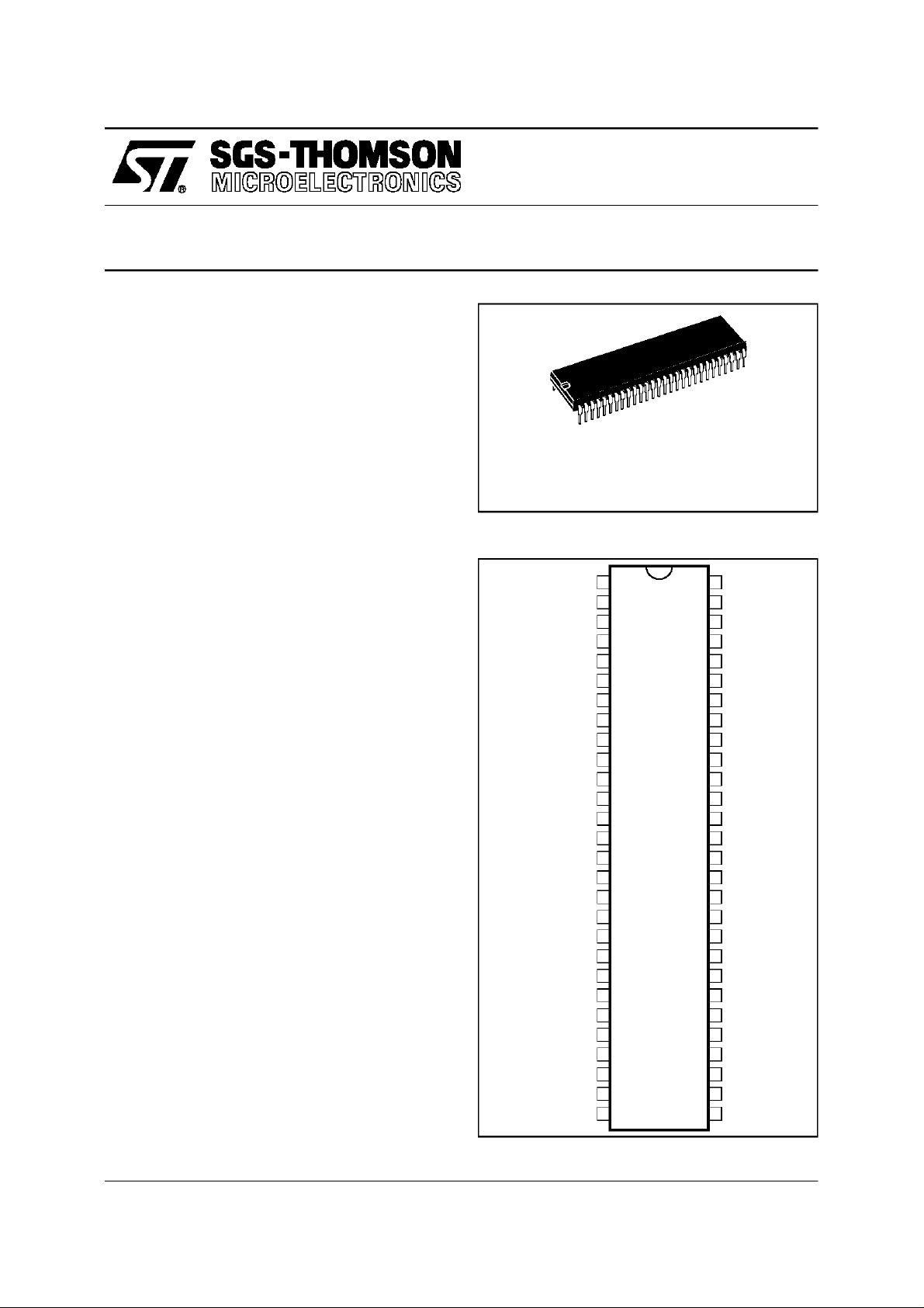
(Plastic Package)
ORDER CODE : STV0056A
PIN CONNECTIONS
FC R
PK IN R
LEVEL R
S1 VID RTN
S3 VID RTN
VOL R
S3 VID OUT
S1 VID OUT
S2 VID OUT
VOL L
S2 VID RTN
S2 OUTL
CLAMP IN
S2 OUT R
UNCLDEEM
VIDEEM2/22kHz
V 12V
VIDEEM1
V GND
B-BAND IN
S2 RTN L
S2 RTN R
FM IN
S3 RTN L
S3 RTN R
AGC L
S3 OUTL
S3 OUT R
STV0056A
SHRINK56
1
2
3
4
5
6
7
8
9
10
11
12
13
14
15
16
17
18
19
20
21
22
23
24
25
26
27
28
ADVANCE DATA
A GND R
56
FC L
55
PK IN L
54
LEVEL L
53
PK OUT L
52
PK OUT R
51
I
50
REF
CPUMP R
49
48
U75 R
47
DET R
46
AMPLK R
45
A 12V
V
44
REF
43
A GND L
42
AGC R
41
AMPLK L
40
U75 L
DET L
39
CPUMP L
38
37
GND 5V
36
VDD5V
35
XTL
J17 L
34
33
J17 R
32
HA
31
SDA
30
SCL
I/O/22kHz
29
0056A-01.EPS
September 1996
This is advance informationon a new product now in development or undergoing evaluation. Detailsare subject to change without notice.
1/26
Page 2

STV0056A
PIN ASSIGNMENT
Pin Number Name Function
1 FC R Audio Roll-off Right
2 PK IN R Noise Reduction Peak Detector Input Right
3 LEVEL R Noise Reduction Level Right
4 S1 VID RTN TV-Scart 1 Video Return
5 S3 VID RTN Decoder-Scart Video Return
6 VOL R Volume Controlled Audio Out Right
7 S3 VID OUT Decoder-Scart Video Output
8 S1 VID OUT TV-Scart 1 Video Output
9 S2 VID OUT VCR-Scart 2 Video Output
10 VOL L Volume Controlled Audio Out Left
11 S2 VID RTN VCR-Scart 2 VideoReturn
12 S2 OUT L Fixed Level Audio Output Left (to VCR)
13 CLAMP IN Sync-Tip ClampInput
14 S2 OUT R Fixed Level Audio Output Right (to VCR)
15 UNCL DEEM Unclamped Deemphasized Video Output
16 VIDEEM2/22kHz Video Deemphasis 2 or 22kHz Output
17 V 12V Video 12V Supply
18 VIDEEM1 Video Deemphasis 1
19 V GND Video Ground
20 B-BAND IN Base Band Input
21 S2 RTN L Auxiliary Audio ReturnLeft (from VCR)
22 S2 RTN R Auxiliary Audio Return Right (from VCR)
23 FM IN FM Demodulator Input
24 S3 RTN L Auxiliary Audio ReturnLeft (from decoder)
25 S3 RTN R Auxiliary Audio Return Right (from decoder)
26 AGC L AGC PeakDetector Capacitor Left
27 S3 OUT L Auxiliary Audio Output L (to decoder)
28 S3 OUT R Auxiliary Audio Output R (to decoder)
29 I/O/22kHz Digital Input/Output or 22kHz Output
30 SCL I
31 SDA I
32 HA Hardware Address
33 J17 R J17 Deemphasis Time Constant Right
34 J17 L J17 Deemphasis Time Constant Left
35 XTL 4/8MHz Quartz Crystal or Clock Input
36 V
5V Digital 5V Power Supply
DD
37 GND 5V Digital Power Ground
38 CPUMP L FM PLL Charge Pump Capacitor Left
39 DET L FM PLL Filter Left
40 U75 L Deemphasis Time Constant Left
41 AMPLK L Amplitude Detector CapacitorLeft
42 AGC R AGC Peak Detector Capacitor Right
43 A GND L Audio Ground
44 V
REF
2
C Bus Clock
2
C Bus Data
2.4V Reference
0056A-01.TBL
2/26
Page 3
PIN ASSIGNMENT (continued)
Pin Number Name Function
45 A 12V Audio 12V Supply
46 AMPLK R Amplitude Detector Capacitor Left
47 DET R FM PLL Filter Right
48 U75 R Deemphasis Time Constant Right
49 CPUMP R FM PLL Charge Pump Capacitor Right
50 I
51 PK OUT R Noise Reduction Peak Detector Output Right
52 PK OUT L Noise Reduction Peak Detector Output Left
53 LEVEL L Noise ReductionLevel Left
54 PK IN L Noise Reduction Peak Detector Input
55 FC L Audio Roll-off Left
56 A GND R Audio Ground
REF
Current Reference Resistor
PIN DESCRIPTION
SOUND DETECTION
FMIN
This is the input to the two FM demodulators. It
feeds two AGC amplifiers with a bandwidth of at
least 5-10MHz. There is one amplifier for each
channelboth withthe same input. The AGCamplifiers havea 0dB to +40dBrange.
=5kΩ, Mininput = 2mVPPpersubcarrier.
Z
IN
Max input = 500mV
(max when all inputs are
PP
added together,when their phasescoincide).
AGC L, AGC R
AGC amplifiers peak detector capacitor connections. Theoutput current has an attack/decay ratio
of 1:32. That is the ramp up current is approximately 5µA and decay current is approximately
160µA. 11Vgives maximum gain. These pins are
also driven by a circuit monitoring the voltage on
AMPLK Land AMPLK R respectively.
AMPLKL, AMPLK R
The outputs of amplitude detectors LEFT and
RIGHT. Each requiresa capacitorand a resistorto
GND. The voltage across this is used to decide
whether thereis a signalbeing received by the FM
detector. The level detector output drives a bit in
the detectorI
2
C bus control block.
AMPLK L and AMPLK R drive also respectively
AGC Land AGC R. For instancewhen thevoltage
on AMPLKL is > (V
frompin AGCLto reducethe AGC gain.
V
REF
+1VBE) it sinkscurrent to
REF
DET L, DETR
Respectivelythe outputsofthe FMphasedetector
left and right.
This is for the connectionof an external loop filter
for the PLL. The output is a push-pull current
source.
CPUMP L, CPUMPR
The output from the frequency synthesizer is a
push-pullcurrentsourcewhichrequiresacapacitor
to groundto derive a voltagetopull the VCO to the
target frequency.The output is ±100µAto achieve
lockand±2µAduringlocktoprovidea trackingtime
constantof approximately10Hz.
V
REF
This is the audio processorvoltagereferenceused
through out the FM/audio section of the chip. As
such it is essential that it is well decoupled to
ground to reduce as far as possible the risk of
crosstalk and noise injection. This voltage is deriveddirectly from the bandgap reference of 2.4V.
The V
output can sink up to 500µA in normal
REF
operationand 100µAwhen in stand-by.
I
REF
Thisisa bufferedV
to produce an accurate current reference, within
the chip, for the biasing of amplifiers with current
outputs into filters.It is alsorequired for the Noise
reduction circuit to provide accurate roll-off frequencies. This pin should not be decoupledas it
would inject current noise. The target current is
50µA±2% thusa 47.5kΩ ±1% is required.
STV0056A
outputto an off-chipresistor
REF
0056A-01.TBL
3/26
Page 4

STV0056A
PIN DESCRIPTION (continued)
A 12V
Double bonded main power pin for the audio/FM
section of the chip.The twobond connectionsare
to the ESD and to power the circuit and on chip
regulators/references.
A GND L
This ground pin is double bonded :
1) to channelLEFT : RF section& VCO,
2) to both AGC amplifiers, channel LEFT and
RIGHTaudio filter section.
A GND R
This ground pin is double bonded :
1) to the volume control, noise reduction system,
ESD + Mux + V
2) to channelright : RF section & VCO
BASEBANDAUDIO PROCESSING
PK OUT L, PK OUT R, PKOUT
The noise reduction control loop peak detector
output requires a capacitorto groundfrom this pin,
and a resistor to V
decaytimeconstant.Anonchip5kΩ ±25%resistor
and externalcapacitor give the attack time.
PK IN L, PK IN R or PK IN
Each ofthesepinsis an inputto acontrollooppeak
detector and is connected to the output of the
offchipcontrol loop bandpass filter.
LEVEL L, LEVELR
Respectivelythe audio left and right signalsof the
FM demodulatorsare output to levelL and level R
pins through an input follower buffer. The off-chip
filters driven by these pins must include AC coupling to the next stage (PK IN L and PKIN R pins
respectively).
FC L, FC R
The variable bandwidth transconductance amplifier hasa current output which is variable depending on the input signal amplitude asdefined bythe
control loop of the noise reduction. The output
current is then dumped into an off-chip capacitor
which togetherwith the accuratecurrentreference
define the min/max rolloff frequencies.Aresistorin
REF
pin to give some accurate
REF
serieswith acapacitoris connectedto groundfrom
these two pins.
J17 L, J17R
The externalJ17 de-emphasisnetworks for channels left and right. The amplifier for this filter is
voltageinput, current output. Output with±500mV
input willbe ±55µA.
To performJ17de-emphasiswiththe STV0042,an
externalcircuit is required.
U75 L, U75 R
External deemphasis networks for channels left
andright.Foreachchannelacapacitorand resistor
in parallel of 75µs time constant are connected
betweenhereandV
toprovide75µs de-empha-
REF
sis. Internallyselectable is an internalresistorthat
canbeprogrammedtobeadded inparallelthereby
convertingthe networkto approx 50µs de-emphasis (see control block map). The valueof the internal resistors is 54kΩ ±30 %. The amplifier for this
filter isvoltageinput, currentoutput ; with±500mV
input the output will be ±55µA.
VOL L, VOL R
The main audio output from the volume control
amplifierthe signal to get output signalsas highas
2V
(+12dB) on a DC bias of 4.8V. Control is
RMS
from +12dB to -26.75dB plus Mute with 1.25dB
steps.Thisamplifierhasshortcircuitprotectionand
is intendedto drivea SCARTconnectordirectlyvia
AC coupling and meets the standardSCARTdrive
requirements. These outputs feature high impedance modefor parallelconnection.
S2 OUT L, S2OUTR, S3 OUT L, S3 OUT R
These audio outputs are sourced directly from the
audio MUX, and as a result do not include any
volume controlfunction. They will output a 1V
RMS
signal biased at 4.8V. They are short circuit protected. These outputs feature high impedance
mode for parallel connection and meet SCART
driverequirement.
S2 RTNL, S2 RTN R, S3RTN L, S3 RTN R
These pins allow auxiliary audio signals to be connected to the audio processor and hence makes
use of the on-chip volume control. For additional
detailsplease referto theaudio switching table.
4/26
Page 5

PIN DESCRIPTION (continued)
VIDEO PROCESSING
B-BAND IN
AC-coupledvideo input from a tuner.
Z
> 10kΩ ±25%. This drives an on-chip video
IN
amplifier. The other input of this amp is AC
grounded by being connected to an internal V
The video amplifier has selectable gain from 0dB
to 12.7dB in 63 steps and its output signal can be
selectednormal or inverted.
UNCL DEEM
Deemphasizedstill unclampedoutput. It isalso an
input of thevideo matrix.
VIDEEM1
Connected to an external de-emphasis network
(forinstance 625 linesPALde-emphasis).
VIDEEM2 / 22kHz
Connected to an external de-emphasis network
(forinstance525 lines NTSC orothervideode-emphasis). Alternativelya precise 22kHztonemaybe
output by I
2
C bus control.
CLAMP IN
This pin clamps the most negative extreme of the
input (the sync tips) to 2.7V
(orappropriatevolt-
DC
age). The video at the clamp input is only 1V
This clamped video which is de-emphasised, filtered andclamped (energy dispersal removed) is
normal, negative syncs, video. This signal drives
the VideoMatrix input called Normal Video.
It hasa weak (1.0µA ±15 %)stable current source
pullingthe inputtowards GND. Otherwisetheinput
impedanceis very high at DC to 1kHz Z
Video bandwidth through this is -1dB at 5.5MHz.
The CLAMPinput DC restore voltageis then used
as a means for getting the correct DC voltage on
the SCARToutputs.
S3 VIDRTN
This input can be driven for instance by the decoder.Thisinputhas aDC restoration clamp on its
input. The clampsink currentis 1µA±15% withthe
buffer Z
>1MΩ.
IN
S2 VIDRTN, S1 VIDRTN
Externalvideoinput1.0V
ACcoupled75Ω source
pp
impedance.This inputhas a DC restoration clamp
on its input. The clamp sink current is 1µA ±15%
with thebuffer Z
>1MΩ. Thissignalis an inputto
IN
the VideoMatrix.
S1 VID OUT, S2VID OUT
Video drivers for SCART 1 and SCART 2. An
external emitter follower buffer is required to drive
>2MΩ.
IN
REF
PP
a 150Ω load. The average DC voltageto be 1.5V
on the O/P. The signalis video2.0V
PP
with sync tip = 1.2V. These pins get signals from
the Video Matrix. The signal selected from the
Video Matrix for output on thispin is controlled by
a control register. This output also feature a high
.
impedancemode for parallelconnection.
S3 VID OUT
This outputcan drive for instancea decoder.Also
it is able to pass 10MHz ; Z
this pin will be 2V
. The black level of the ouput
PP
<75Ω. Video on
OUT
video signal can be adjustedthrough I
trol to easily interface with on-board Videocrypt
decoder. This output feature an high impedance
mode for parallelconnection.
V 12V
+ 12Vdoublebonded: ESD+guardrings andvideo
circuitpower.
V GND
Doubledbonded.CleanVIDIN GND. Strategically
placed video power ground connection to reduce
video currents gettinginto the rest of the circuit.
CONTROLBLOCK
GND 5V
.
The main power ground connection for the control
logic, registers, the I
2
C bus interface, synthesizer
& watchdogand XTLOSC.
V
5V
DD
Digital +5V power supply.
SCL
ThisistheI
2
C busclockline.Clock= DCto100kHz.
Requiresexternal pull up eg.10kΩ to 5V.
SDA
This is the I
2
C bus dataline.Requiresexternalpull
up eg. 10kΩ to 5V.
I/O / 22kHz
Generalpurpose input outputpin or 22kHz output.
XTL
This pinallowsforthe on-chiposcillator tobe either
used witha crystal to groundof 4MHzor 8MHz, or
to be driven by an external clock source. The
external source can be either 4MHz or 8MHz. A
programmablebitinthecontrolblockremovesa÷2
blockwhen the 4MHz optionis selected.
HA
Hardwareaddress with internal135µApull down.
Chip address is 06 when this pin is grouded and
chip address is 46 when connected to V
STV0056A
5.5MHzBW
2
C buscon-
.
DD
5/26
Page 6
STV0056A
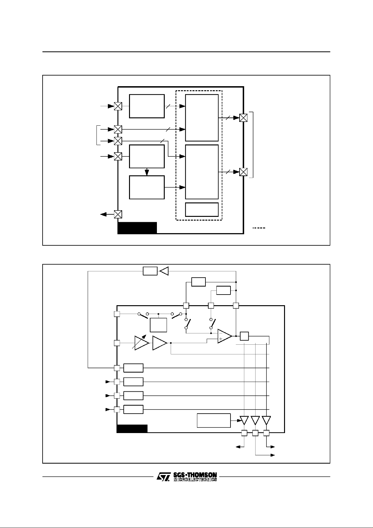
GENERALBLOCK DIAGRAM
From Tuner
Vide o
Proce ssing
From TV,
VCR/Decode r
FM
B-BAND
From Tuner
Demodulation
2 Cha nnels
Wegener
Panda +
Dee m phas is
22kHz to LNB
STV0056A
VIDEO PROCESSINGBLOCK DIAGRAM
LPF
2
6x3
Video
4
Matrix
3
2
To TV, VCR/De coder
Audio
Matrix
3
+
Volume
2
CBus
I
Interface
Active in Stand-by
0056A-02.EPS
6/26
I/O/22kHz
B-BAND IN
CLAMP IN
S3 VID RTN
S2 VID RTN
S1 VID RTN
29
20
CLAMP
13
CLAMP
5
CLAMP
11
CLAMP
4
STV0056A
NTSC
PAL
VIDEEM1VIDEEM2/22kHz
16 18 15
22kHz
TONE
± 1
G
Baseband
Normal
DecoderReturn
VCR Return
TV Return
BLACK LEVEL
ADJUST
To Decoder To VCR
UNCL DEEM
Deemphasized
2
89
7
S1 VID OUT
S2 VID OUTS3 VID OUT
To TV
0056A-03.EPS
Page 7
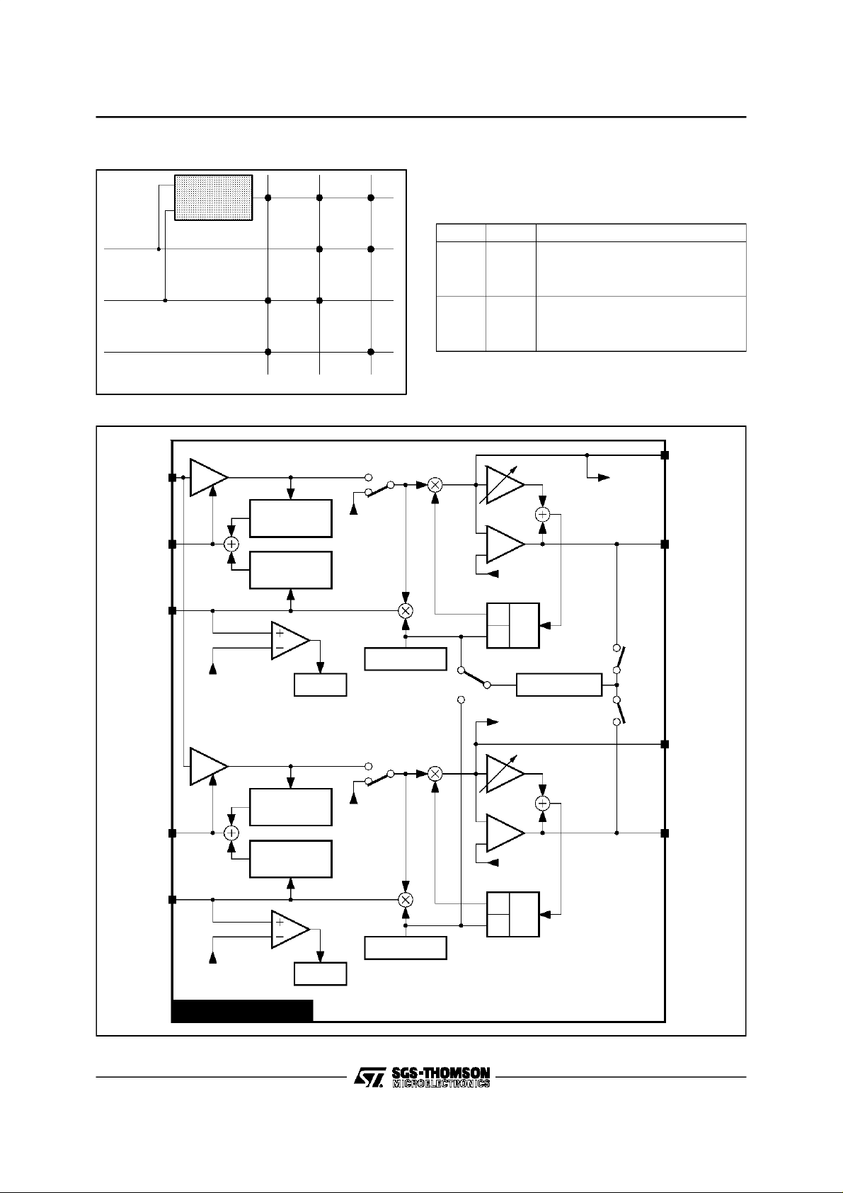
AUDIO PROCESSINGBLOCK DIAGRAM (CHANNELRIGHT)
AUDIO R
47
a
ANRS
K3
K4
abc
K6
28 25 51 2 3 1 14 22 6
b
a
-6dB -6dB
b
4
AUDIO
DEEMPHASIS
33 48
STV0056A
K2
a
ba
c
abc
6dB6dB
K1
b
c
K5
MONO
STEREO
STV0056A
DET R
PLL
FILTER
DecoderOut
FC R
PK IN R
S3 OUT R
Audio
DECODER VCR
S3 RTN R
Audio
DecoderReturn
LEVEL R
PK OUT R
J17 R
U75 R
AUDIO PROCESSING BLOCK DIAGRAM (CHANNEL LEFT)
AUDIO L
39
a
ANRS
K3
K4
abc
K6
27 24 52 54 53 55 12 21 10
b
a
-6dB -6dB
b
4
AUDIO
DEEMPHASIS
32 40
S2 OUT R
S2 RTN R
STV0056A
K2
a
ba
c
abc
6dB6dB
K1
b
c
K5
MONO
STEREO
VOL R
TV
0056A-04.EPS
DET L
PLL
FILTER
Audio
Decoder Out
FC L
PK IN L
S3 OUT L
DECODER VCR
S3 RTN L
Audio
Decoder Return
LEVEL L
PK OUT L
J17 L
U75 L
S2 OUT L
S2 RTN L
VOL L
TV
0056A-05.EPS
7/26
Page 8
STV0056A
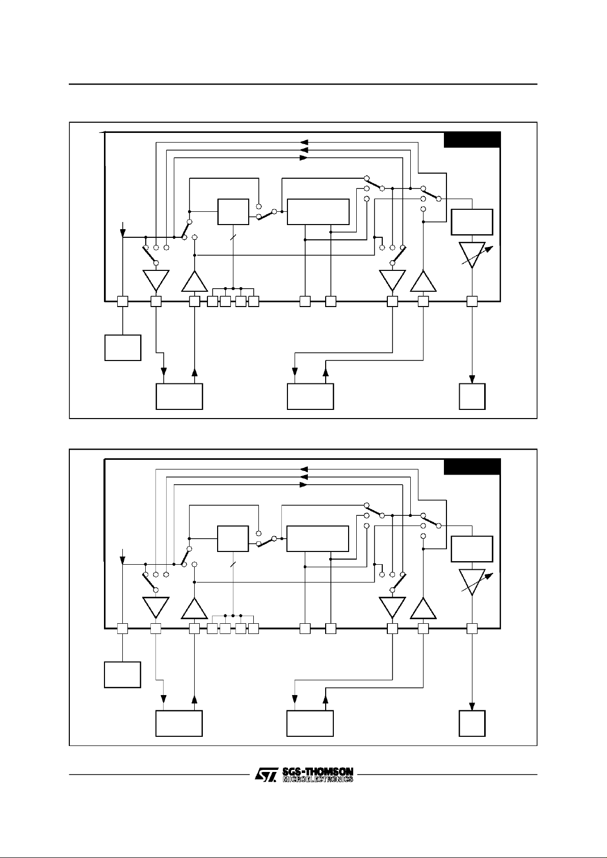
AUDIO SWITCHING
AUDIO
DEEMPHASIS
+ ANRS
AUDIOPLL
DECRTN
AUXIN K
K
1a
K
1b
1c 6b
VOL OUT AUX OUT
K
K
K
5b
5c
5a
FMDEMODULATION BLOCK DIAGRAM
FM IN
AGC R
AGC
LEVEL
DETECTOR1
LEVEL
DETECTOR2
Bias
K
6c
K
6a
K
DECOUT
SW1
K
4
0056A-06.EPS
Phase
Detect
:a→ANRSinput non-scrambledaudio
b → ANRS input descrambledaudio
K
a
b
b
c
a
b
b
c
K
2
1
2
1
2
3
a
No ANRS, No De-emphasis
a
No ANRS, 50µs
a
No ANRS, 75µs
a
No ANRS, J17
b
ANRS, No De-emphasis
b
ANRS, 50µs
b
ANRS, 75µs
b
ANRS, J17
DETR
AUDIOR
FM dev.
Select.
CPUMPR
V
REF
AMPLKR
AGC L
AMPLKL
V
AGC
V
REF
REF
Reg8 b4
LEVEL
DETECTOR1
LEVEL
DETECTOR2
Reg8 b0
Amp. Detect
WATCHDOG
SW3
Bias
Amp. Detect
WATCHDOG
Phase
Detect
90
VCO
0
SYNTHESIZER
AUDIOL
FM dev.
Select.
V
REF
90
VCO
0
SW2
SW4
DETL
CPUMPL
8/26
STV0042/STV0056A
0056A-07.EPS
Page 9

CIRCUIT DESCRIPTION
STV0056A
Video Section
The compositevideo is first set to a standardlevel
by means of a 64 stepgain controlled amplifier. In
the casethatthemodulationisnegative,aninverter
can be switchedin.
One of two different external video de-emphasis
networks (for instance PAL and NTSC) is selectable by anintegrated bus controlled switch.
Then energy dispersal is removed by a sync tip
clamping circuit, which is used on all inputs to a
video switching matrix, thus making sure that no
DC stepsoccur when switching video sources.
The matrix can be used to feed video to and from
decoders, VCR’sand TV’s.
A bus controlled black level adjustment circuit is
provided on the decoder output allowing a direct
connectionto an on-board Videocryptdecoder.
Additionaly all the video outputs are tristate type
(high impedance mode is supported), allowing a
simple parallel connections to the scarts (Twin
tuner applications).
AudioSection
The two audio channels are totally independent
except for the possibility given to output on both
channelsonly oneoftheselectedinputaudiochannels.
To allow a very cost effective application, each
channel uses PLL demodulation.Neither external
complexfilter nor ceramicfilters are needed.
The frequency of the demodulated subcarrier is
chosen by a frequencysynthesizerwhich sets the
frequency of the internal local oscillator by comparing its phase with the internally generated
reference. When the frequency is reached, the
microprocessor switches in the PLL and the demodulationstarts.Atanymomentthemicroprocessor can read from the device(watchdog registers)
the actualfrequency to whichthe PLLis locked.It
canalsoverifythatacarrierispresentatthewanted
frequency(byreading AMPLKstatus bit) thanksto
a synchronous amplitude detector, which is also
used forthe audio input AGC.
In order to maintain constant amplitude of the
recovered audio regardless of variations between
satellitesor subcarriers, the PLL loop gain may be
programmedfrom56 values.
Any frequency deviation can be accomodated
(from ±30kHz till ±400kHz).
Two different networks can be permanently connectedfor either75µs or J17 de-emphasis. If 50µs
de-emphasisis required,thiscan be insertedbyan
internal switch, thus allowing a worldwide application.
The STV0056A is intended to be compatible with
WegenerPanda System.
Twotypes of audio outputsare provided: oneis a
fixed 1V
2V
RMS
and the other is a gain controlled
RMS
max. The control range beingfrom +12dB
to -26.75dBwith1.25dBsteps.Thisoutputcanalso
be muted.
A matrixis implementedto feed audio toand from
decodersVCR’s andTV’s.
Noise reduction system and de-emphasis can be
inserted or by-passedthrough bus control.
Also all the audio outputs are tristate-type (high
impedancemode is supported), allowing a simple
parallelconnectionstothescarts (Twintunerapplications).
Others
A22kHz toneis generated for LNB control.
It isselectablebybus controland available on one
of the two pins connected to the external video
de-emphasis networks. One general purpose I/O
is alsoavailable on the STV0056A.
By means of the I
2
C bus there is the possibility to
drive the ICs into a low powerconsumption mode
with active audio and v ideo matrixes. Independantly from the main power mode, each individualaudio andvideooutputcan bedrivento high
impedancemode.
9/26
Page 10

STV0056A
ABSOLUTEMAXIMUM RATINGS
Symbol Parameter Value Unit
V
CC
V
DD
P
tot
T
oper
T
stg
THERMALDATA
Symbol Parameter Value Unit
Rth(j-a) Thermal ResistanceJunction-ambient Max. 55
DC AND AC ELECTRICAL CHARACTERISTICS
=12V,VDD=5V,T
(V
CC
Symbol Parameter Test Conditions Min. Typ. Max. Unit
V
CC
V
DD
IQ
CC
IQ
DD
IQLP
CC
IQLP
DD
AUDIO DEMODULATOR
FMIN FM Subcarrier Input Level
DETH Detector 1 and 2 (AMPLOCK Pins)
VCOMI VCO Mini Frequency V
VCOMA VCO Maxi Frequency 10 MHz
AP50 1kHz Audio Level at PLL output
APA50 1kHz Audio Level at PLL output
FMBW FM Demodulator Bandwidth Gain at 12kHz versus 1kHz
DPCO Digital Phase Comparator Output
AUTOMATIC NOISE REDUCTION SYSTEM
LRS Output Level (Pins LEVEL) 1V
LDOR Level Detector Output Resistance
NDFT Level Detector Fall Time Constant
NDLL Bias Level (Pins PK OUT) No audio in 2.40 V
LLCF NoiseReduction Cut-off Frequencyat
HLCF Noise Reduction Cut-off Frequency at
Supply Voltage 15
7.0
Total Power Dissipation 900 mW
Operating Ambient Temperature 0, + 70
Storage Temperature -55, + 150
=25oC unless otherwise specified)
amb
Sypply Voltage 11.4
4.75125.0
Supply Current All audio and all videooutputs
12.6
5.25VV
5587015mA
activated
Supply Current at Low Power Mode All audio and all videooutputs
276359mA
are in high impedance mode
(Pin FMIN for AGC action)
VCO locked on carrier at 6MHz
560kΩ load onAMPLOCK Pins
5 500 mV
180kΩ load onDET Pins
(Threshold for activating Level Detector 2)
(DET Pins)
(DET Pins)
8mVPP≤ FMIN ≤ 500mV
Carrier without modulation
: 11.4 to 12.6V,
CC
: 0 to 70oC
T
amb
0.5V
50kHz dev. FM input,
PP
Coarse deviation set to 50kHz
(Reg. 05 = 36
HEX
PP
)
0.5VPP50kHz dev. FM input,
Coarse and fine settings used
2.90 3.10 3.30 V
5MHz
0.6 1 1.35 V
0.92 1 1.08 V
0 0.3 1 dB
180kΩ, 82kΩ 22pFon DET Pins
Current (CPUMP Pins)
Average sink and source
current to external capacitor
on left and rightchannel 0.9 1 1.1 V
PP
60 µA
4.0 5.4 6.8 kΩ
(Pins PK OUT)
(Pins PK OUT)
Low Level Audio
High Level Audio
External 22nF to GND and
1.2MΩ to V
100mV
capacitor 330pF (FC Pins)
1V
PP
capacitor 330pF (FC Pins)
REF
onDET Pins, External
PP
on DET Pins, External
26.4 ms
0.85 kHz
7 kHz
o
V
V
o
C
o
C
C/W
mA
mA
PP
PP
PP
0056A-03.TBL
0056A-04.TBL
PP
0056A-05.TBL
10/26
Page 11

STV0056A
DC AND AC ELECTRICAL CHARACTERISTICS (continued)
=12V,VDD=5V,T
(V
CC
Symbol Parameter Test Conditions Min. Typ. Max. Unit
AUDIO OUTPUT (Pins VOL OUT R, VOL OUT L)
DCOL DC Output Level 4.8 V
AOLN Audio Output Level
with Reg 00= 1A
AOL50 Audio Output Level
with Reg 00= 1A
AOL75 Audio Output Level
with Reg 00= 1A
AOL17 Audio Output Level
with Reg 00= 1A
AMA1 Audio Output Attenuation
with Mute-on. Reg 00 = 00.
MXAT Max Attenuation before Mute.
Reg 00 = 01.
MXAG Audio Gain. Reg 00 =1F. 1kHz, from S2 RTN Pins 5 6 7 dB
ASTP Attenuation of each of the 31
steps
THDA1 THD with Reg 00 = 1A 1V
THDA2 THD with Reg 00 = 1A 2V
THDFM THD with Reg 00 = 1A FM input as for APA50
ACS Audio Channel Separation 1V
ACSFM Audio Channel Separation at 1kHz - 0.5 V
SNFM Signal to Noise Ratio FM input as for APA50,
SNFMNR Signal to Noise Ratio FM input as for APA50
Z
Z
OUT H
OUTL
Audio Output Impedance Low impedance mode
AUXILIARY AUDIO OUTPUT (Pins S2 OUT R, S2 OUT L, S3 OUT R, S3 OUT L)
DCOLAO DC output level Aux. inputpins open circuit 4.8 V
AOLNS Audio Output Level
on S2 and S3
AOL50S Audio Output Level
on S2 and S3
AOL75S Audio Output Level
on S2 and S3
AOL17S Audio Output Level
on S2 and S3
AGAO S2 to S3Audio Gain
and S3 to S2 Audio Gain
THDA02 THD on S2, Input inS3 2V
=25oC unless otherwise specified)
amb
FM input as for APA50
No de-emphasis, No pre-emphasis
No noise reduction
FM input as for APA50
50µs de-emphasis, 27kΩ//2.7nF load
No pre-emphasis, No noise reduction
FM input as for APA50
75µs de-emphasis, 27kΩ//2.7nF load
No pre-emphasis, No noise reduction
FM input as for APA50
J17 de-emphasis, 36kΩ 4.7kΩ 8.2nF load
No pre-emphasis, No noise reduction
1VPP- 1kHz from S2 RTN Pins 60 65 dB
1kHz, from S2 RTN Pins 32.75 dB
1kHz 1.25 dB
-1kHz fromS2 RTN Pins 0.15 %
PP
-1kHz fromS2 RTN Pins 0.3 1 %
PP
75µs de-emphasis, ANRS ON
-1kHz on S2 RTN Pins 60 74 dB
PP
- 50kHz deviation FM input on
PP
one channel
- 0.5V
no deviation FM input on the
PP
other channel
- Reg 05 = 36
-75µs de-emphasis, no ANRS
75µs de-emphasis,
no ANRS, Unweighted
75µs de-emphasis,
ANRS ON, Unweighted
High impedance mode 301844 55ΩkΩ
FM input as for APA50
No de-emphasis, No pre-emphasis
No noise reduction
FM input as for APA50
50µs de-emphasis, 27kΩ//2.7nF load
No pre-emphasis, No noise reduction
FM input as for APA50
75µs de-emphasis, 27kΩ//2.7nF load
No pre-emphasis, No noise reduction
FM input as for APA50
J17 de-emphasis, 36kΩ 4.7kΩ 8.2nF load
No pre-emphasis, No noise reduction
1kHz -1 0 +1 dB
- 1kHz from Aux input pins 0.04 0.2 %
PP
1.5 1.9 2.34 V
2.0 3.3 4.0 V
2.0 3.3 4.0 V
2.0 3.2 4.0 V
0.3 1 %
60 dB
HEX
56 dB
69 dB
1.55 2 2.42 V
2.0 3.4 4.0 V
2.0 3.4 4.0 V
2.0 3.3 4.0 V
PP
PP
PP
PP
PP
PP
PP
PP
0056A-06.TBL
11/26
Page 12

STV0056A
DC AND AC ELECTRICAL CHARACTERISTICS (continued)
=12V,VDD=5V,T
(V
CC
Symbol Parameter Test Conditions Min. Typ. Max. Unit
AUXILIARY AUDIO OUTPUT (Pins S2 OUT R, S2 OUT L, S3 OUT R, S3 OUT L) (continued)
THDAOFM THD on S2 orS3 FM input as for APA50
Z
OUT L
Z
OUT H
Audio Output Impedance Low impedance mode
I/O
V
V
V
V
OH
LNB
LNB
OL
Low Level Input
IL
High Level Input 2.4
IH
Low Level Output
High Level Output
Tone Frequency 22.2 22.2 22.2 kHz
T
Tone Signal Duty Cycle No load connected onI/O 49 50 51 %
D
RESET
RTCCU End of Reset Threshold for V
RTCCD Start of Reset Threshold for V
RTDDU End of Reset Threshold for V
RTDDD Start of Reset Threshold for V
COMPOSITE SIGNAL PROCESSING
VIDC VID IN External load current < 1µA 2.25 2.45 2.65 V
ZVI VID IN Input Impedance 7 11 14 kΩ
DEODC DC Output Level (Pins VIDEEM) 2.25 2.45 2.65 V
DEOMX Max AC Level before Clipping
(Pins VIDEEM)
DGV Gain error vs GV @ 100kHz GV = 0to 12.7dB, Reg 01 = 00 → 3F -0.5 0 0.5 dB
INVG Inverter Gain -0.9 -1 -1.1
VISOG Video Input to SCART Outputs
Gain
DEBW Bandwidth for 1V
measured on Pins VIDEEM
DFG Differential Gain on Sync Pulses
measured on Pins VIDEEM
ITMOD Intermodulation of FM subcar-
riers with chroma subcarrier
CLAMP STAGES (Pins CLAMP IN, S1, S2, S3 VID RTN)
ISKC Clamp Input Sink Current V
ISCC Clamp Input Source Current V
VIDEO MATRIX
XTK Output Level on any Output
when 1V
selected for any other output
PP
BFG OutputBuffer Gain (PinsS1 VID
OUT,S2 VID OUT,S2 VIDOUT)
DCOLVH DC Output Level High impedance mode 0 0.2 V
Z
OUT HV
Video Output Impedance High impedance mode 16 23 30 kΩ
VCL Sync Tip Level on Selected
Outputs (Pins S1 VID OUT, S2
VID OUT)
VCL S3 Sync Tip Level at S3 VID OUT
with Black Level Adjust
=25oC unless otherwise specified)
amb
75µs de-emphasis, no ANRS
High impedance mode 306044
I
= 2mA
sink
= 2mA 3.2
I
source
CCVDD
CCVDD
DDVCC
DDVCC
= 5V, VCCgoing up 8.7 V
= 5V, VCCgoing down 7.9 V
= 12V, VDDgoingup 3.8 V
= 12V, VDDgoingdown 3.5 V
GV = 0dB,Reg 01 = 00 2 V
De-emphasis amplifier mounted in unity
gain, Normal video selected
PP
input
@ - 3dBwith GV = 0dB,Reg 01 = 00 10 MHz
GV = 0dB, 1V
25Hz sawtooth (input : VID IN)
7.02 and 7.2MHz sub-carriers,
12.2dB lower than chroma
= 3V 0.5 1 1.5 µA
IN
=2V 405060µA
IN
@ 5MHz -60 dB
CVBS input is
@ 100kHz 1.87 2 2.13
CVBS through 10nF on input 1.05 1.3 1.55 V
1V
PP
Register 4
b6 b7
00
01
10
11
CVBS + 0.5V
PP
PP
0.3 1 %
10055Ω
0.8 V
0.2
0.4 V
4.6
-1 0 1 dB
1%
-60 dB
1.36
1.52
1.67
1.84
kΩ
V
V
V
V
V
V
PP
0056A-07.TBL
12/26
Page 13

PIN INTERNAL CIRCUITRY
S1 VIDRTN, S2 VIDRTN, S3 VID RTN,
CLAMP IN
50µA source is active only when VIDIN < 2.7V.
Figure 1
9V
V
DD
50µA
STV0056A
UNCL DEEM
Sameas abovebut with no black level adjustment
and slightly different gain.
Figure4
Ω
60
V
12V
CC
S1 VID RTN
S2 VID RTN
S3 VID RTN
CLAMPIN
10k
1µA
Ω
1
1
V
5V
DD
GND0V
S3 VID OUT
I blacklevelisI
2
Cprogrammablefromsource16µA
to sink 33µA equivalent to an offset voltage of
-150mV to + 300mV.
The 60Ω collector resistor is for short cct. protec-
tion.
Figure2
60Ω
VCC12V
4
S3 VID OUT
VIDMUX 10kΩ
2.3mA
GND 0V
16.7kΩ
GND0V
25kΩ
I Black Level
V
2.4V
REF
4
IN 10k
0056A-08.EPS
2.3mA
GND 0V
VIDEEM1
Ron of the transistor gate is ≈10kΩ.
Figure5
6µ/2µ
10µ/2µ
VIDEEM1
VIDEEM2/ 22kHz
Ron of the transistor gate is ≈10kΩ.
0056A-09.EPS
Ω
25k
16.7kΩ
GND 0V
Ω
UNCL DEEM
V
REF
1
125µA
2.4V
0056A-11.EPS
0056A-12.EPS
S1 VID OUT, S2 VID OUT
Same as above but withnoblack leveladjustment.
Figure3
60Ω
4
VID MUX 10kΩ
2.3mA
GND 0V
V
CC
20kΩ
GND 0V
12V
20kΩ
S1 VID OUT
S2 VID OUT
V
2.4V
REF
Figure6
VIDEEM2/22kHz
0056A-10.EPS
6µ/2µ
10µ/2µ
100µ/2µ
60µ/2µ
1
125µA
V
5V
DD
22kHz
0056A-13.EPS
13/26
Page 14

STV0056A
PIN INTERNAL CIRCUITRY (continued)
VID IN
Figure7
V
2.4V
REF
10kΩ
VID IN
6.5k
Ω
0.5pF
GND0V
1
+
85µA
S2 OUT L, S2 OUT R, S3 OUT L, S3 OUT R
Sameas above but with gain fixed at +6dB.
Figure11
S2 OUT L
S2 OUT R
S3 OUT L
S3 OUT R
0056A-14.EPS
Audio
2.4V Bias
20kΩ
20kΩ
PK OUTR, PK OUT L
Figure8
Audio
PeakDetector
VDD9V
1
1
3.4V
5kΩ
Clamp
PK OUTR
PK OUTL
FC L, FC R
Ivar is controlled by the peak det audio level max.
±15µA (1V
PP
audio).
Figure9
V
9V
DD
FC L
FC R
Ivar
1
1
GND 0V
S2 RTNL, S2 RTN R, S3 RTN L, S3 RTN R
4.8V bias voltageis the same as the bias level on
the audiooutputs.
Figure12
25k
0056A-15.EPS
S2 RTN L
S2 RTN R
S3 RTN L
S3 RTN R
4.8V
Ω
1
50µA
FM IN
Theotherinputforeachchannelisinternallybiased
in the sameway via 10kΩ to the 2.4V V
REF
Figure13
10kΩ
10kΩ
Left Channel
1
0056A-16.EPS
2.4V
FM IN
0056A-18.EPS
0056A-19.EPS
.
VOL OUT R, VOL OUT L
Audio output with volume and scart driver with
+12dB of gain for up to 2V
. The opamp has a
RMS
push-pulloutput stage.
Figure10
14/26
Audio
2.4V Bias
30kΩ
15kΩ
30kΩ
GND 0V
4.8V
VOL OUT R
VOL OUT L
Right Channel
I
REF
The optimum value if I
1
50µA
is 50µA ±2% so an
REF
externalresistor of 47.5kΩ ±1%is required.
Figure14
2.4V
1
0056A-17.EPS
I
REF
50µA
0056A-20.EPS
0056A-21.EPS
Page 15

PIN INTERNAL CIRCUITRY (continued)
I/O / 22kHz
The input is TTL compatible.
The outputis tri-stateable.
Figure15
STV0056A
HA
Pull-downcurrent for SDIP42.
Inputwith CMOSlevels.
Figure19
10µ/2µ
IIC Reg
91µ/2µ
MUX
22kHz
180µ/2µ
100µ/2µ
I/O/22kHz
205
ESD
Ω
SCL
This is the input toa Schmittinputbuffermadewith
a CMOS amplifier.
Figure16
Ω
205
SCL 24µ/4µ
ESD
SDA
Input same as above.
Output pull down only : relies on external resistor
for pull-up.
Figure17
25µ/2µ
10µ/2µ
GND 0V
0056A-22.EPS
HA
205Ω
ESD
150µA
XTL
Figure20
XTL
0056A-23.EPS
750µA
460Ω
232
500µA
460Ω
5pF
GND 0V
CPUMP L, CPUMP R
An offseton the PLLloop filter will cause an offset
in the two 1µA currents that will prevent the PLL
fromdrifting-off frequency.
Figure21
0056A-26.EPS
3
750µA
0056A-27.EPS
SDA
205
Ω
24µ/4µ
600µ/2µ
ESD
GND0V
J17 L, J17 R, U75 L, U75R
I1 - I2 = 2 xaudio / 18kΩ.
eg 1V
audio : ±55µA.
PP
The are internalswitches to match theaudio level
of the differentstandards.
Figure18
J17 L
J17 R
U75 L
U75 R
I1
I2
100µA
CPUMP L
CPUMP R
Dig Synth
0056A-24.EPS
100µA
DET L, DET R
I2 - I1 = f (phaseerror).
Figure22
0056A-25.EPS
1µA
Loop Filter Tracking
1µA
VCO Input
0056A-28.EPS
I2
DET L
DET R
I1
0056A-29.EPS
15/26
Page 16

STV0056A
PIN INTERNAL CIRCUITRY (continued)
AMPLK L, AMPLK R, AGC L, AGC R
I2 and I1 from the amplitude detecting mixer.
Figure23
To VCA
I2
AMPLK L
AMPLKR
V
REF
2
I1
10kΩ
V
2.4V
REF
The 400µAsource is offduring stand-bymode.
Figure24
Vbg 1.2V
4
10kΩ
10kΩ
GND 0V
LEVEL L, LEVEL R
Figure25
V
2.4V
REF
SW
Audio
49kΩ49kΩ
50kΩ
1
5µA
160µA
400µA
100µA
V
REF
AGC L
AGC R
(2.4V)
LEVEL R
LEVEL L
VGND
Doubled bonded:
- Onepad is connectedtopower-up allof thevideo
mux and I/O.
- The second pad is only as a low noise GND for
the videoinput.
5V,GND 5V
V
DD
Connected to XTL oscillator and the bulk of the
CMOSlogic and 5V ESD.
A GND
Doubled bonded:
0056A-30.EPS
- One pad connected to the left VCO, dividers,
mixers and guard ring. the guard connectionis
star connecteddirectly to the pad.
- Thesecond pad is connected to both AGCamps
and the deemphasis amplifiers, frequency synthesisand FM deviation selectioncircuit for both
channels.
A 12V
Doubled bonded:
- One pad connectedto theESD and guardring.
- Thesecond pad is connected to the mainpower
for all of the audio parts.
0056A-31.EPS
A GND R
Boubled bonded :
- One pad connected to the right VCO, dividers,
mixers and guard ring. The guard connection is
star connecteddirectly to the pad.
- The second pad is connected to the bias block,
audio noisereduction,volume, muxand ESD.
A third bond wire on this pin is connecteddirectly
to the diepad (substrate).
Figure27
0056A-32.EPS
PK IN L, PK IN R
Figure26
V
2.4V
REF
PK IN R
PK IN L
67k
1
To Peak Det
Ω
100µA
V 12V
Doubledbonded (twobond wiresandtwo padsfor
one packagepin) :
- One pad is connectedto all of the 12V ESD and
video guard rings.
- The second pad is connected to power up the
video block.
16/26
BIP10vpl
0056A-33.EPS
V GND
VDD5V
Vpp
Vmm
GND 5V
A GNDL
Substrate
A GND R
V 12V
VideoPads
DigitalPads
A 12V
AudioPads
205Ω
BIP
12V
DZPN1
DZPN1
DZPN1
+
-
0056A-34.EPS
Page 17

STV0056A
I2C PROTOCOL
1) WRITING to the chip
S-Start Condition
P-StopCondition
CHIP ADDR - 7 bits. Programmable06H or 46H (STV0056Aonly) with Pin HA.
W-Write/Read bit is the 8th bit of the chip address.
A-ACKNOWLEDGEafter receiving8 bitsof data/adress.
REG ADDR Addressof register to be writtento, 8 bits of whichbits 3, 4, 5, 6 & 7 are ’X’or
don’t care ie
DATA 8 bitsof databeingwritten totheregister. All8 bitsmustbewrittentoatthe same
time.
REG ADDR/A/DATA/A can be repeated, the write process can continue untill terminated with a STOP
condition.If the REGADDR is higher than 07 then IIC PROTOCOLwill still be
met (ie an A generated).
Example :
S06WA00A55A01A8F A P
2) READING from the chip
Whenreading,there is anauto-incrementfeature.Thismeans anyreadcommandalwaysstarts by reading
Reg 8 and will continue to read the following registersin orderafter each acknowledgeor until there is no
acknowledge or a stop. This function is cyclic that is it will read the same set of registers without
re-addressingthe chip.There are two modes of operation as set by writing to bit 7 ofregister 0. Read3
registersin a cyclicfashionor all 5 registers in a cyclicfashion.Note onlythe last 5 of the 11registers can
be read.
Reg0 bit 7 =L ⇒ Start/ chipadd /R / A/ Reg8 / A/ Reg9 / A/ Reg 0A/ A/ Reg8 / A/ Reg9 /A /Reg 0A
/... / P /
Reg0 bit 7 =H ⇒ Start / chip add /R / A/ Reg 8 /A / Reg 9 / A/ Reg0A / A/ Reg 7 / A/ Reg 6 / A / Reg 8
/ A/ Reg 9 / A / Reg 0A/ A/ Reg 7 / A/ Reg 6 /... / P /
only the first 3 bitsare used
.
CONTROLREGISTERS
Reg 0 write only
Bit (default 00
HEX
)
0 L Select 5 bits audio volumecontrol 00H = MUTE
1 L Select 5 bits audio volumecontrol 01H = -26.75dB
2 L Select 5 bits audio volumecontrol : : : : :
3 L Select 5 bits audio volumecontrol 1.25dBsteps up to
4 L Select 5 bits audio volumecontrol 1FH = +12dB
5 L Audio mux switchK4 - ANRSI/P select (L = PLL)
6 L Audio mux switchK3 - ANRSselect (L = no ANRS,H = ANRS)
7 L L = read 3 registers, H = read5 registers
Reg 1 write only
Bit (default 00
HEX
)
0 L Select video gain bits
1 L Select video gain bits 00H = 0dB
2 L Select video gain bits 01H = +0.202dB
3 L Select video gain bits 02H = +0.404dB
4 L Select video gain bits n = + 0.202dB * n
5 L Select video gain bits 3FH = +12.73 dB
6 L Selected videoinvert (H = inverted,L = non inverted)
7 L Video deemphasis 1 / Videodeemphasis2 (L: V
De-em1)
ID
17/26
Page 18

STV0056A
CONTROLREGISTERS (continued)
Reg 2 write only
Bit (default F7
0 H Select video sourcefor scart 1 O/P
1 H Select video sourcefor scart 1 O/P
2 H Select video sourcefor scart 1 O/P
3 L Select 4.000MHz or 8.000MHz clock speed (L= 8MHz)
4 H Select audio sourcefor volume output (SwitchK1)
5 H Select audio sourcefor volume output (SwitchK1)
6 H Select Left/Right/Stereofor volume output
7 H Select Left/Right/Stereofor volume output
Reg 3 write only
Bit (default F7
0 H Select video sourcefor scart 2 O/P
1 H Select video sourcefor scart 2 O/P
2 H Select video sourcefor scart 2 O/P
3 L Video deemphais2 / 22kHz(H : 22kHz)
4 H Select audio sourcefor Scart 2 output (SwitchK5)
5 H Select audio sourcefor Scart 2 output (SwitchK5)
6 H Audio deemphasisselect (Switch K2)
7 H Audio deemphasisselect (Switch K2)
HEX
HEX
)
)
Reg 4 write only
Bit (default BF
HEX
)
0 H Select source forvideo decoderO/P
1 H Select source forvideo decoderO/P
2 H Select source forvideo decoderO/P
3 H Stand-byor lowpower mode (H = low power)
4 H Select audio sourcefor Scart 3 output (SwitchK6)
5 H Select audio sourcefor Scart 3 output (SwitchK6)
6 L Black leveladjust on Scart3 video
7 H Black leveladjust on Scart 3 video
Reg 5 write only
Bit (default B5
HEX
)
0 H FM deviation selection-- defaultvalue for 50kHz modulation
1 L FM deviation selection
2 H FM deviation selection
3 L FM deviation selection
4 H FM deviation selection
5 H FM deviation selection(L = double the FM deviation)
6 L Select 22kHz for I/O (Pin 29 / STV0056A)
7 H Select TP50a (H) or I/O (Pin 29 / STV0056A).TP50afor testonly.
Reg 6 write/read
Bit (default 86
HEX
)
0 L Status of I/O
1 H Select data direction of I/O1 (H = output)
2 H Select frequency synthesizer1 OFF/ON(L = OFF)
3 L Select frequency synthesizer2 OFF/ON(L = OFF)
4 L Select RF source (L = OFF) to FM det 1
5 L Select RF source (L = OFF) to FM det 2
6 L Select frequency for PLLsynthesizer - LSB (bit 0) of 10-bit value
7 H Select frequency for PLLsynthesizer - bit1 of 10-bit value
18/26
Page 19

CONTROLREGISTERS (continued)
Reg 7 write/read
Bit (defaultAF
HEX
)
0 H Select frequency for PLLsynthesizer - bit2 of 10-bit value
1 H Select frequency for PLLsynthesizer
2 H Select frequency for PLLsynthesizer
3 H Select frequency for PLLsynthesizer
4 L Select frequency for PLLsynthesizer
5 H Select frequency for PLLsynthesizer
6 L Select frequency for PLLsynthesizer
7 H Select frequency for PLLsynthesizer - bit9, MSB (10th bit) of 10-bit value
Reg 8 read only
Bit
0 Subcarrierdetection (DET 1) (L = Nosubcarrier)
1 Not used
2 Read frequencyof watchdog1 - LSB (bit0) of 10-bit value
3 Read frequencyof watchdog1 - bit 1 of 10-bit value
4 Subcarrierdetection (DET 2) (L = Nosubcarrier)
5 Not used
6 Read frequencyof watchdog2 - bit 0 of 10-bit value
7 Read frequencyof watchdog2 - bit 1 of 10-bit value
STV0056A
Reg 9 read only
Bit (defaultAF
HEX
)
0 Read frequencyof watchdog1 - bit 2 of 10-bit value
1 Read frequencyof watchdog1
2 Read frequencyof watchdog1
3 Read frequencyof watchdog1
4 Read frequencyof watchdog1
5 Read frequencyof watchdog1
6 Read frequencyof watchdog1
7 Read frequencyof watchdog1 - bit 9, MSB (10th bit) of 10-bit
Reg 0A read only
Bit
0 Read frequencyof watchdog2 - bit 2 of 10-bit value
1 Read frequencyof watchdog2
2 Read frequencyof watchdog2
3 Read frequencyof watchdog2
4 Read frequencyof watchdog2
5 Read frequencyof watchdog2
6 Read frequencyof watchdog2
7 Read frequencyof watchdog2 - bit 9, MSB (10th bit) of 10-bit
19/26
Page 20

STV0056A
CONTROLREGISTERS (continued)
Video Mux Truth Tables
Register2 <0:2> ⇒ Scart 1 videooutput control
Register3 <0:2> ⇒ Scart 2 videooutput control
Register4 <0:2> ⇒ Scart 3decoder output control
The truthtable for the threescart outputs are the same.
Register 2/3/4 Video Output
Bit<2>
0
0
0
0
1
1
1
1
Bit <7>
Bit<1>
0
0
1
1
0
0
1
1
Register 4 Black Level Adjust on Scart 3
0
1
0
1
Bit<0>
Bit <6>
0
0
1
1
0
Baseband video
1
De-emphasized video
0
Normal video
1
Scart 3 return
0
Scart 2 return
1
Scart 1 return
0
Nothing selected
1
High Z or low power (default)
-150mV
0 (default)
+150mV
+300mV
AudioMux Truth Tables
Register 2 Switch K1/Audio Source Selection for Volume Output
Bit <5>
0
1
0
1
Bit <7>
0
1
0
1
Bit <6>
0
1
X
X
Bit <5>
0
1
0
1
Bit <4>
0
0
1
1
Register 3 Switch K2/Audio Deemphasis
Bit <6>
0
0
1
1
Register 0 Switch K3 & K4
Bit <5>
X
X
0
1
Register 3 Switch K5/Audio Source Selection for Scart 2
Bit <4>
0
0
1
1
Volume Output
A
Audio deemphasis (K2 switch O/P)
C
Scart 2 return
B
Scart 3 return
-
High Z or low power (default)
Audio Deemphasis
A
No deemphasis
C
J17
B
50µs
B
75µs (default)
ANRS I/O Select
A
Noise reduction OFF
B
Noise reduction ON (default)
A
I/P = PLL
B
I/P = Scart3 return
Aux Audio Output
C
PLL output
A
Scart 3 return
B
Audio deemphasis (K2 switch O/P)
-
High Z or low power state(default)
20/26
Bit <5>
0
1
0
1
Register 4 Switch K6/Audio Source Selection for Scart 3
Bit <4>
0
0
1
1
Audio Decoder Output
A
PLL output
C
Audio deemphasis (K2 switch O/P)
B
Scart 2 return
-
High Z or low power state(default)
Page 21

CONTROLREGISTERS (continued)
Register 2 Left / Right/ Stereo on Volume Output
Bit <7>
0
1
1
Bit <6>
0
0
1
Mono left / channel 1
Mono right / channel 2
Stereo left & right (default)
Register 5 : FM DeviationSelection
43210
0
0
0
0
0
0
0
0
0
0
0
0
0
0
0
0
1
1
1
1
1
1
1
1
1
1
1
1
1
1
1
1
Example : Default power up state 54.4kHz ⇒±54.4kHz.
0
0
0
0
0
0
0
0
1
1
1
1
1
1
1
1
0
0
0
0
0
0
0
0
1
1
1
1
1
1
1
1
0
0
0
0
1
1
1
1
0
0
0
0
1
1
1
1
0
0
0
0
1
1
1
1
0
0
0
0
1
1
1
1
0
0
1
1
0
0
1
1
0
0
1
1
0
0
1
1
0
0
1
1
0
0
1
1
0
0
1
1
0
0
1
1
0
1
0
1
0
1
0
1
0
1
0
1
0
1
0
1
0
1
0
1
0
1
0
1
0
1
0
1
0
1
0
1
Selected Nominal Carrier Modulation
Bit 5 = 0 Bit 5 = 1
Do not use
Do not use
Do not use
Cal. set. (2V)
592kHz
534kHz
484kHz
436kHz
396kHz
358kHz
322kHz
292kHz
266kHz
240kHz
218kHz
196kHz
179kHz
161kHz
146kHz
122kHz
120kHz
109kHz
98kHz
89kHz
78kHz
71kHz
65kHz
58kHz
53kHz
48.6kHz
43.8kHz
39.6kHz
cal : do not use = 0.3373V offset on VCO
cal : do not use = 0.3053V offset on VCO
cal : do not use = 0.2763V offset on VCO
calibration setting (1V offset on VCO)
296kHz modulation
267kHz modulation
242kHz
218kHz
198kHz
179kHz
161kHz
146kHz
133kHz
120kHz
109kHz
98.3kHz
89.7kHz
80.9kHz
73.1kHz
66.0kHz
60.0kHz
54.4kHz = default power up state
49.1kHz
44.3kHz
39.8kHz
35.9kHz
32.4kHz
29.1kHz
26.7kHz
24.3kHz
21.9kHz
19.7kHz
STV0056A
Register 1
Bit <7>
0
0
1
1
Register 5 Digital I/O (STV0056A pin 29)
Bit <7>
0
0
1
1
Register 3
Bit <3>
0
1
0
1
Bit <6>
0
1
0
1
Video Deemphasis/22kHz
Deemphasis 1 (default)
Deemphasis 1 + 22kHz
Deemphasis 2
Deemphasis 2
I/O (refer to Register 6 Bit <0> Bit <1>)
22kHz
Do not use (for test only) (default)
22kHz
21/26
Page 22

STV0056A
FM DEMODULATION SOFTWARE ROUTINE
With theSTV0056Acircuit, for eachchannel,three
steps are requiredto acheive a FM demodulation :
st
-1
step:To setthe demodulationparameters:
• FM deviation selection,
• Subcarrier frequency selection.
nd
step : To implement a waiting loop to check
-2
the actualVCO frequency.
rd
step:To closethedemodulationphaselocked
-3
loop (PLL).
Refering to the FM demodulation block diagram
(page 12), the frequency synthesis block is common to bothchannels(leftandright); consequently
1st STEP (LEFT) : SETTINGTHE DEMODULATION PARAMETERS
A. TheFM deviationis selected by loading R5with
the appropriatevalue. (see R5 truth table).
NB : Very wide deviations(up to ±592kHz)can be
accomodatedwhen R5 B5is low.
Corresponding bandwidth can be calculated as
follows :
Bw ≈ 2 (FM deviation + audiobandwidth)
Bw ≈ 2 (value given in table+ audio bandwidth)
In the example:
R5Bits 7 6 543210
XX110110
B. The subcarrier frequency is selected by
launchinga frequencysynthesis(theVCOis driven
to the wanted frequency). This operation requires
two actions:
- To connect the VCO to the frequency synthesis
loop.Referingtothe FMblockdiagram(page12):
• SW4 closed ⇒ R6B2 = H
• SW3 to bias ⇒ R6 B4 = L
• SW2 to bias
⇒ R6B3 = L
• SW1 opened ⇒ R6 B5 = L
- To load R7 and R6 B6 B7 with the value corre-
sponding to the left channel frequency. This 10
bitsvalue is calculatedas follows:
Subcarrierfrequency= coded valuex 10kHz
(10kHz is the minimum step of the frequency
synthesisfunction)
Consideringthat the tunning rangeis comprised
between5to 10MHz,thecodedvalueisanumber
between500 and 1000(2
10
= 1024) then 10 bits
are required.
Example:
7.02MHz= 702 x 10kHz
702 ⇒ 10101111 10 ⇒ AF + 10
R7 isloaded with AF and R6 B6 : L, R6 B7: H.
two completesequenceshaveto be doneone after
the other when demodulatingstereo pairs.
Detailed Description
Conventions:
- R = Standsfor Register
- B = Stands for Bit
Example:
R05 B2 = Register 05, Bit 2
For clarity, the explanationsare based on the following example : stereo pa ir 7 .02MHz/L
7.20MHz/R, deviation±50kHz max.
The Table1 givesthe setting for themost common
subcarrierfrequencies.
Table 1 :Frequency Synthesis Register Setting
for the Most Common Subcarrier Frequencies
Subcarrier Frequency
(MHz)
5.58 8B 1 0
5.76 90 0 0
5.8 91 0 0
5.94 94 1 0
6.2 9B 0 0
6.3 9D 1 0
6.4 A0 0 0
6.48 A2 0 0
6.5 A2 1 0
6.6 A5 0 0
6.65 A6 0 1
6.8 AA 0 0
6.85 AB 0 1
7.02 AF 1 0
7.20 B4 0 0
7.25 B5 0 1
7.38 B8 1 0
7.56 BD 0 0
7.74 C1 1 0
7.85 C4 0 1
7.92 C6 0 0
8.2 CD 0 0
8.65 D8 0 1
Register 7
(Hex)
Register 6
Bit 7 Bit 6
22/26
Page 23

FM DEMODULATION SOFTWARE ROUTINE (continued)
2ndSTEP (LEFT) :
VCO FREQUENCYCHECKING (VCO)
This secondstepis actuallya waitingloop in which
the actual runningfrequency of the VCO is measured.
To exit of this loop is allowed when : Subcarrier
Frequency- 10kHz≤ Measured Frequency≤ Subcarrier Frequency + 10kHz (± 10kHz is the maximum dispersion of the frequency synthesis
function).
In practice, R8 B2 B3 and R9 are read and compared to the value loaded in R6 B6 B7 and R7
±1 bit.
Note :
The duration of this stepdepends on how large is
frequency difference between the start frequency
and the targeted frequency. Typically:
- the rateofchangeof the VCO frequencyis about
3.75MHz/s(C
pump
=10µF)
- In addition to this settling time, 100ms must be
addedto takeinto accountthesamplingperiodof
the watchdog.
In practice:
- SW3 closed ⇒ R6B4 = H
- SW4 opened ⇒ R6 B2 =L
After this sequence of 3 steps for left channel,
a similar sequenceis neededfor the right channel.
Note :
In the sequencefor the right, there is no need to
again select the FMdeviation (once is enough for
the pair).
General Remark
Before to enable the demodulated signal to the
audiooutput,it isrecommandedto keepthe muting
and tocheck whethera subcarrieris present atthe
wantedfrequency.Suchaninformationisavailable
in R8 B0 and R8 B4 whichcan be read.
Two differentstrategies canbe adoptedwhenenabling the output :
- Eitherboth leftandright demodulatedsignals are
simultaneously authorized when both channel
are ready.
- Orwhile therightchannelsequenceisrunning,the
already readyleftsignalis sentto theleft andright
3rdSTEP (LEFT)
TheFMdemodulationcanbestartedbyconnecting
the VCO to the phase locked loop (PLL).
outputs and the real stereo sound L/R is output
when bothchannelsare ready.This secondoption
givessound a few hundredsof ms before the first
one.
STV0056A
23/26
Page 24

STV0056A
TYPICALAPPLICATION(3 SCARTS, PAL/SECAMEuropeApllication)
TV SCART
VCR SCART
C4
C101
220nF
R6
220nF
R102
J6RJ5
21 J1
20
19
18
17
16
15
14
13
12
11
10
9
8
7
6
5
4
3
2
1
R5 68Ω
75Ω
21 J2
20
19
18
17
16
15
14
13
12
11
10
9
8
7
6
5
C5
2.2µF
4
3
2
1
C6
C8
2.2µF
2.2µF
C7
2.2µF
75Ω
J4
L
V
CCV
R2 68Ω
V
Q1
BC547
R3
470Ω
C2
2.2µF
C3
2.2µF
CCV
V
Q101
BC547
R101
CCV
V
470Ω
Q2
BC547
R4
470Ω
R9 5.1kΩ
C12 100pF
R10 10kΩ
8.2nF
3
1
SEL5618
R11 1.5kΩ
R16
1kΩ
2
C11
TDK FILTER
Ω
R100
75
R59
1.2MΩ
C65
100nF
C64
1.5nF
R58
C100
220nF
43kΩ
1231617181920 111213141521
4589
JP12
67
VIDEO MATRIX
AND
10
MATRIX
AUDIOSTEREO
CCV
+
C13
10µF 16V
V
C26
10µF
16V
VIDEO
BROADBAND
PROCESSOR
22232425262728
NOISE REDUCTION
FM
TWO-CHANNEL
DEMODULATOR
DEEMPHASIS
R15 1kΩ
C
2
I
DECODER
R54
3.3kΩ
R55
1.5kΩ
C61
1.5nF
C62
100nF
1.5nF
8.2nF
C63
220nF
C115
220nF
R117
C114
R114
3.3kΩ
24kΩ
8.2nF
R56
R116
R115
Q4
BC557
10kΩ
CCA
V
10kΩ
Q103
BC557
C113
1.5nF
1.5kΩ
R57
24kΩ
R60
1.2MΩ
C66
R53
43kΩ
55
C60
5453
C112
100nF
R113
52
51343332
C50
10µF
16V
1%
R50
+
47.5kΩ
CCA
V
C42
100nF
C43
100nF
R36
560kΩ
40 41 47 48 4942 43 44 45 46 50 563938373635
C41
10µF
16V
+
DD
V
C29
22pF
4MHz or
8MHz Crystal
560kΩ
R41
82kΩ
C48
22pF
C47
R51
C58
100nF
R37
560kΩ
C45
100nF
22pF
560kΩ
R40
180kΩ
C46
2.7nF
R39
27kΩ
C40
470µF
16V
+
R34
27kΩ
C39
2.7nF
R33
180kΩ
C38
22pF
C37
R32
22pF
82kΩ
R106
36kΩ
C108
R107
8.2nF
4.7kΩ
SEL5618 :5MHz LPF made by TDK / Japan
24/26
DECODER SCART
R105
36kΩ
C107
R104
8.2nF
4.7kΩ
CCA
V
C34
100nF
C35
220µF
16V
+
22kHz
GENERATOR
1I/O
J8
1
J9
INPUT
CLOCK
313029
DD
V
CCV
V
C30
100nF
C32
C65
47pF
+
C66
47pF
SDA
SCL
4
GND
15V
J11
123
J10
5V
100nF
C31
220µF
16V
C33
220µF
16V
+
L1 22µH
1
1
112V
J12
J14
J13 L2 22µH
GND
GND
21 J3
20
R103 68Ω
19
18
17
16
15
14
13
12
11
10
9
8
7
6
5
4
3
2
1
C104
C103
C102
2.2µF
2.2µF
C105
2.2µF
2.2µF
C23
8.2nF
C56
100nF
L4
47µH
C24
27pF
R18
1kΩ
R17 470Ω
C25
100pF
R48
75Ω
J7
INPUT
TUNER
STV0056A
0056A-35.EPS
Page 25

STV0056A
TWIN TUNER APPLICATION
Easy parallelconnectionof the outputs to the scarts withoutany additionalswitchinghardware.
This configuration is possible due to the high impedancemode that canbe selectedfor each audio and
video outputs.
2
I C Bus
TUNER1
TUNER2
5V
32
32
S
T
V
A
S
T
V
A
8
9
7
0
0
5
6
0
0
5
6
6-10
12-14
27-28
8
9
7
6-10
12-14
27-28
Video
TV
SCART
Audio
2
Video
VCR
SCART
Audio
2
Video
DECODER
SCART
Audio
2
25/26
0056A-36.EPS
Page 26

STV0056A
PACKAGE MECHANICALDATA
56 PINS- PLASTICSHRINK DIP
Dim.
Min Typ Max Min Typ Max
A 5.08 0.200
A1 0.51 0.020
B 0.35 0.59 0.014 0.023
B1 0.75 1.42 0.030 0.056
C 0.20 0.36 0.008 0.014
D 52.12 2.052
D1––––––
E 18.54 0.730
E1 13.72 0.540
K1––––––
K2––––––
L 2.54 3.81 .100 0.150
e1 1.78 0.070
N56
mm inches
Number of Pins
PMSDIP56.WMF
SDIP56.TBL
Information furnishedis believed to be accurateand reliable. However, SGS-THOMSON Microelectronics assumes no responsibility
for the consequences of use of such information nor for anyinfringement of patents or other rights of third partieswhich may result
from its use. Nolicence isgranted by implication or otherwise under any patent or patentrights of SGS-THOMSON Microelectronics.
Specifications mentioned in this publication are subject to change without notice. This publication supersedes and replaces all
information previouslysupplied. SGS-THOMSON Microelectronics products are not authorized for use as critical components in life
support devices or systems without express written approval of SGS-THOMSON Microelectronics.
1996 SGS-THOMSON Microelectronics - All Rights Reserved
Purchase of I
2
I
C Patent. Rights to use these components in a I2C system,is granted provided that the systemconformsto
Australia - Brazil -Canada - China -France - Germany - Hong Kong - Italy -Japan - Korea- Malaysia - Malta - Morocco
The Netherlands - Singapore - Spain - Sweden - Switzerland - Taiwan - Thailand - United Kingdom -U.S.A.
2
C Components of SGS-THOMSON Microelectronics, conveys a license under the Philips
2
the I
C Standard Specifications as defined by Philips.
SGS-THOMSON Microelectronics GROUP OF COMPANIES
26/26
 Loading...