

Page 1
SATELLITESOUNDAND VIDEO PROCESSORS
SOUND
.
TWO INDEPENDENTSOUNDDEMODULATORS
.
PLL DEMODULATION WITH 5-10MHz
FREQUENCY SYNTHESIS
.
PROGRAMMABLE FM DEMODULATOR
BANDWIDTH ACCOMODATING FM DEVIATIONSFROM±30kHz TILL±400kHz
.
PROGRAMMABLE 50/75µs OR NO DE-EMPHASIS
.
DYNAMICNOISEREDUCTION
.
ONE OR TWO AUXILIARY AUDIO INPUTS
ANDOUTPUTS
.
GAIN CONTROLLED AND MUTEABLE
AUDIOOUTPUTS
.
HIGH IMPEDANCE MODE AUDIO OUTPUTS
FORTWINTUNER APPLICATIONS
VIDEO
.
COMPOSITE VIDEO 6-bit 0 to 12.7dB GAIN
CONTROL
.
COMPOSITE VIDEO SELECTABLE INVERTER
.
TWO SELECTABLE VIDEO DE-EMPHASIS
NETWORKS
.
4 x 2 VIDEOMATRIX
.
HIGH IMPEDANCE MODE VIDEO OUTPUTS
FORTWINTUNER APPLICATIONS
MISCELLANEOUS
.
22kHzTONEGENERA TI ONFORLNBCONTROL
.
I2C BUS CONTROL :
CHIPADDRESSES= 06
.
LOW POW ER STAND-BYMODEWITH ACTIVE
AUDIO ANDVIDEOMATRIXES
DESCRIPTION
TheSTV0042ABICMOSintegratedcircuitrealizes
all the necessarysignal processingfrom the tuner
to the Audio/Video input and output connectors
regardlessthe satellite system.
The STV0042 is intended for low cost satellite
receiverapplication.
HEX
(Plastic Package)
ORDER CODE : STV0042A
PIN CONNECTIONS
FC R
PK IN
SUM OUT
VOL R
S1 VID OUT
S2 VID OUT
VOL L
S2 VID RTN
S2 OUT L
CLAMP IN
S2 OUT R
UNCL DEEM
VIDEEM2/22kHz
V 12V
VIDEEM1
V GND
B-BANDIN
S2 RTN L
S2 RTN R
FM IN
STV0042A
PRODUCT PREVIEW
SHRINK42
1
2
3
4
5
6
7
8
9
10
11
12
13
14
15
16
17
18
19
20
21 22
A GND R
42
FC L
41
PK OUT
40
I
39
REF
CPUMP R
38
U75 R
37
DET R
36
AMPLK R
35
A 12VA 12V
34
V
33
32
31
30
29
28
27
26
25
24
23
REF
A GND L
AGC R
AMPLK L
U75 L
DET L
CPUMP L
GND 5V
5V
V
DD
XTL
SDA
SCLAGC L
0042A-01.EPS
March 1997
1/24
Page 2
STV0042A
PIN ASSIGNMENT
Pin Number Name Function
1 FC R Audio Roll-off Right
3 SUM OUT Noise Reduction Summing Output
2 PK IN Noise Reduction Peak Detector Input
4 VOL R Volume Controlled Audio Out Right
5 S1 VID OUT TV-Scart 1 Video Output
6 S2 VID OUT VCR-Scart 2 Video Output
7 VOL L Volume Controlled Audio Out Left
8 S2 VID RTN VCR-Scart2 VideoReturn
9 S2 OUT L Fixed Level Audio Output Left
10 CLAMP IN Sync-Tip Clamp Input
11 S2 OUTR Fixed Level Audio Output Right
12 UNCL DEEM Unclamped Deemphasized Video Output
13 VIDEEM2/22kHz Video Deemphasis 2 or 22kHz Output
14 V 12V Video 12V Supply
15 VIDEEM1 Video Deemphasis 1
16 V GND Video Ground
17 B-BAND IN Base Band Input
18 S2 RTN L Auxiliary Audio Return Left
19 S2 RTN R Auxiliary Audio Return Right
20 FM IN FM Demodulator Input
21 AGC L AGC Peak Detector Capacitor Left
22 SCL I
23 SDA I
24 XTL 4/8MHz QuartzCrystal or Clock Input
25 V
5V Digital 5V Power Supply
DD
26 GND 5V Digital Power Ground
27 CPUMP L FM PLL Charge Pump Capacitor Left
28 DET L FM PLL Filter Left
29 U75 L Deemphasis Time Constant Left
30 AMPLK L Amplitude Detector Capacitor Left
31 AGC R AGC Peak Detector Capacitor Right
32 A GND L Audio Ground
33 V
REF
34 A 12V Audio 12V Supply
35 AMPLK R Amplitude Detector Capacitor Left
36 DET R FM PLL Filter Right
37 U75 R Deemphasis Time Constant Right
38 CPUMP R FM PLL Charge Pump CapacitorRight
39 I
REF
40 PK OUT Noise Reduction Peak Detector Output
41 FC L Audio Roll-off Left
42 A GND R Audio Ground
2
C Bus Clock
2
C Bus Data
2.4V Reference
Current Reference Resistor
0042A-01.TBL
2/24
Page 3

PIN DESCRIPTION
1 - Sound Detection
FMIN
This is the input to the two FM demodulators. It
feeds two AGC amplifiers with a bandwidth of at
least 5-10MHz. There is one amplifier for each
channelboth with the sameinput.TheAGCamplifiers have a 0dB to +40dBrange.
=5kΩ, Min input =2mVPPper subcarrier.
Z
IN
Max input = 500mV
(max when all inputs are
PP
addedtogether,when their phases coincide).
AGC L, AGC R
AGC amplifiers peak detector capacitor connections.The outputcurrent has an attack/decayratio
of 1:32. That is the ramp up current is approximately 5µA and decay current is approximately
160µA. 11V gives maximumgain. These pins are
also driven by a circuit monitoring the voltage on
AMPLKL andAMPLK R respectively.
AMPLKL, AMPLK R
The outputs of amplitude detectors LEFT and
RIGHT.Eachrequiresa capacitorand a resistorto
GND. The voltage across this is used to decide
whetherthereis a signalbeing receivedby the FM
detector.The level detector output drives a bit in
the detectorI
2
C bus control block.
AMPLK L and AMPLK R drive also respectively
AGCL and AGC R. For instance when thevoltage
on AMPLK L is > (V
V
frompin AGCLto reduce the AGCgain.
REF
+1VBE) it sinks current to
REF
DET L, DETR
Respectivelythe outputsof the FMphasedetector
left and right. This is for the connection of an
external loop filter for the PLL. The output is a
push-pullcurrent source.
CPUMPL, CPUMPR
The output from the frequency synthesizer is a
push-pullcurrentsourcewhichrequiresa capacitor
togroundto derivea voltageto pullthe VCOto the
targetfrequency.The output is ±100µAto achieve
lockand ±2µAduringlocktoprovidea trackingtime
constantof approximately10Hz.
VREF
Thisisthe audio processorvoltagereferenceused
through out the FM/audio section of the chip. As
such it is essential that it is well decoupled to
ground to reduce as far as possible the risk of
crosstalk and noise injection. This voltage is derived directly from the bandgapreference of 2.4V.
The V
output can sink up to 500µA in normal
REF
operationand 100µAwhen in stand-by.
IREF
Thisis abufferedV
outputto an off-chipresistor
REF
to produce an accurate current reference, within
STV0042A
the chip, for the biasing of amplifierswith current
outputs into filters.It is also required for the Noise
reduction circuit to provide accurate roll-off frequencies.
This pin should not be decoupled asit would inject
currentnoise.The targetcurrentis 50µA±2%thus
a 47.5kΩ ±1% is required.
A 12V
Double bonded main power pin for the audio/FM
section of the chip. The two bond connectionsare
to the ESD and to power the circuit and on chip
regulators/references.
A GND L
This ground pin is double bonded :
1) to channel LEFT : RF section & VCO,
2) to both AGC amplifiers, channel LEFT and
RIGHTaudio filter section.
A GND R
This ground pin is double bonded :
1) to the volume control, noise reduction system,
ESD + Mux + V
2) to channel right : RF section& VCO
2 - BasebandAudioProcessing
PK OUT
The noise reduction control loop peak detector
outputrequiresa capacitorto groundfrom this pin,
and a resistor to V
decaytimeconstant.Anon chip5k
and externalcapacitor give the attack time.
PK IN
This pin is an inputto a controlloop peak detector
andis connectedto theoutputof the offchipcontrol
loop bandpass filter.
SUM OUT
The two audio demodulated signals are summed
togetherbymeansofanamplifierwithagainof0.5.
If both inputs are 1V then the output is 1V. This
amplifierhas an input followerbufferwhich givesa
offset in the DC bias voltage. Thus the filter
V
BE
which this amplifier drives must include AC coupling to the next stage (PK IN Pin).
FC L, FC R
The variable bandwidth transconductance amplifier has a currentoutput which is variabledepending on the input signalamplitude as definedby the
control loop of the noise reduction. The output
current is then dumped into an off-chip capacitor
whichtogetherwith the accurate current reference
definethe min/maxrolloff frequencies.Aresistorin
serieswitha capacitorisconnectedto ground from
these two pins.
REF
pin to give some accurate
REF
Ω ±
25%resistor
3/24
Page 4

STV0042A
PIN DESCRIPTION(continued)
U75 L, U75 R
Exter naldeemphasi snetwor k s for channels left and
right. For each channel a capaci t or and resistor in
parallelof 75µ stimeconstantare connect edbetween
hereandV
select abl e is an internal resis tor that can be programmedtobeaddedinparal lelthere byconvertingthe
netwo r ktoapprox50µsde-emphasis(seecontro lblock
map ).Thevalueoftheinter nalresistorsis30k Ω ±30%.
Theampli fi erforthisfilterisvoltageinput,currentoutput;
with ±500m Vinputtheoutputwil lbe±55 µ A.
VOLL, VOL R
Themainaudiooutputfromthevol umecontrolamplifier
the signal to get output signals as high as 2V
(+12dB)ona DCbiasof4.8V.Controlisfrom+12dBto
-26.7 5dBplus Mute with 1.25dBsteps.Thisamplifi er
has short circuit protection and is intended to drive a
SCARTconnectordirectlyvia AC coupli n gandmeets
thestandar dSCARTdri v erequi rements.Thes eoutpu ts
featur ehighimped ancemodeforparallelconnection.
S2 OUT L, S2 OUT R
These audio outputs are sourced directl y from the
audioMUX,andas aresultdonotincludeanyvolume
controlfunction.Theywilloutputa1V
at4.8V .Theyareshortcircui tprotected.Theseoutputs
featurehigh impedancemodefor parallelconnectio n
andmeetSCARTdriverequirement.
S2 RTN L, S2 RTN R
Thesepins allowauxiliary audiosignals to be connected to the audio processor and hence makes
use of the on-chip volume control. For additional
detailsplease refer to the audio switching table.
3 - VideoProcessing
B-BAND IN
AC-coupledvideo input from a tuner.
Z
>10k
IN
fier.TheotherinputofthisampisACgroundedbybeing
connectedtoaninterna lV
selectablegainfrom0dBto12.7dBin63stepsandits
outputsignalcanbe selectednormalorinverted.
UNCLDEEM
Deemphasizedstill unclamped output.It isalso an
input of thevideo matrix.
VIDEEM1
Connected to an external de-emphasis network
(forinstance 625 lines PALde-emphasis).
VIDEEM2/ 22kHz
Connected to an external de-emphasis network
(forinstance525lines NTSCor othervideode-emphasis).Alternativelyaprecise22kHztone maybe
output by I
CLAMPIN
Thispinclampsthemostnegativeextremeoftheinput
(thesynctips) to2.7V
4/24
toprov i d e75µsde-emph as i s.Internally
REF
signalbiased
RMS
Ω ±
25%.Thisdrivesanon-chipvideoampli-
.Thevideoamplifierhas
REF
2
C bus control.
(orappropriat evoltage) .The
DC
RMS
video at the clamp input is only 1V
.Thisclamped
PP
video which is de-e mph as i s ed,filter ed and clamped
(energydispersa lremoved)isnormal,negativesyncs,
video.Thissignaldrivesthe VideoMatrixinputcalled
Normal Video. It has a weak (1.0µA ±15 %) stable
currentsourcepullingtheinput toward sGND .Otherwise theinput impedanceis veryhigh atDC to 1kHz
>2MΩ. Video bandwidth through this is -1dB at
Z
IN
5.5MHz.TheCLAMPinputDCrestorevoltageis then
usedasameansforgettingthecorrectDCvoltageon
theSCARToutputs.
S2 VID RTN
External video input 1.0VPPAC coupled 75
Ω
sourceimpedance.This input hasa DCrestoration
clamp on its input. The clamp sink current is 1µA
±
15% withthe bufferZ
>1MΩ. Thissignal is an
IN
input to the VideoMatrix.
S1 VID OUT,S2 VID OUT
VideodriversforSCART1andSCART2.Anexternal
emitterfollowerbufferisrequiredto drivea 150 Ωload.
TheaverageDC voltageto be 1.5V on the O/P.The
signalisvideo2.0V
5.5MHzBWwithsynctip=1.2V.
PP
These pins get signals from the Video Matrix. The
signalselectedfromtheVideoMatri xforoutputon this
piniscontrolledbya controlregister.Thisoutputalso
featureahighimpedancemodeforparallelconnection.
V 12V
+12Vdoublebonded : ESD+guardringsand video
circuitpower.
V GND
Doubledbonded.Clean VID INGND. Strategically
placed video power ground connection to reduce
video currents getting into the rest of the circuit.
4 - Control Block
GND 5V
The main power ground connectionfor the control
logic, registers, the I
2
C bus interface, synthesizer
& watchdog and XTLOSC.
VDD 5V
Digital +5V powersupply.
SCL
Thisis theI2C busclockline.Clock= DCto100kHz.
Requiresexternal pull up eg. 10kΩto 5V.
SDA
This is the I2Cbus dataline. Requires externalpull
up eg. 10kΩ to5V.
XTL
Thispinallowsfor theon-chiposcillatorto beeither
used with a crystaltoground of 4MHzor 8MHz, or
to be driven by an external clock source. The
external source can be either 4MHz or 8MHz. A
programmablebitinthecontrolblockremovesa÷2
block when the 4MHzoption is selected.
Page 5
GENERAL BLOCK DIAGRAM
STV0042A
From Tuner
Video
Processing
From
VCR/Decoder
FM
B-BAND
From Tuner
Demodulation
2 Channels
Noise
Reduction+
Deemphasis
22kHzto LNB
STV0042A
VIDEOPROCESSINGBLOCK DIAGRAM
LPF
2
4x2
Video
2
Matrix
2
1
To TV, VCR/Decoder
Audio
Matrix
2
+
Volume
2
I
C Bus
Interface
Active in Stand-by
0042A-02.EPS
B-BAND IN
CLAMP IN
S2 VID RTN
17
CLAMP
10
CLAMP
8
STV0042A
NTSC
PAL
VIDEEM1VIDEEM2/22kHz
13 15 12
22kHz
TONE
± 1
G
Baseband
Normal
VCR / Decoder Return
To Decoder or VCR To TV
UNCL DEEM
Deemphasized
÷ 2
56
S1 VID OUTS2 VID OUT
0042A-03.EPS
5/24
Page 6
STV0042A
AUDIO PROCESSINGBLOCK DIAGRAM(CHANNEL RIGHT)
STV0042A
K2a
K1a
PK IN
5
SUM OUT
a
K3
b
FC L
FC R
ANRS
AUDIO R
-6dB
36 19 40 2 3 1 41 37 11 4
DET R
PLL
FILTER
PK OUT
S2 RTN R
DECODER OR VCR
AUDIO
DEEMPHASIS
U75 R
AUDIO PROCESSINGBLOCK DIAGRAM(CHANNELLEFT)
b
c
MONO
STEREO
bc
K5
6dB
VOL R
S2 OUT R
TV
0042A-04.EPS
STV0042A
K2a
K1a
6/24
b
c
bc
K5
6dB
S2 OUT L
PK IN
5
SUM OUT
a
K3
b
FC L
FC R
ANRS
AUDIO L
-6dB
28 18 40 2 3 1 41 29 9 7
DET L
PLL
FILTER
PK OUT
S2 RTN L
DECODER OR VCR
AUDIO
DEEMPHASIS
U75 L
MONO
STEREO
VOL L
TV
0042A-05.EPS
Page 7
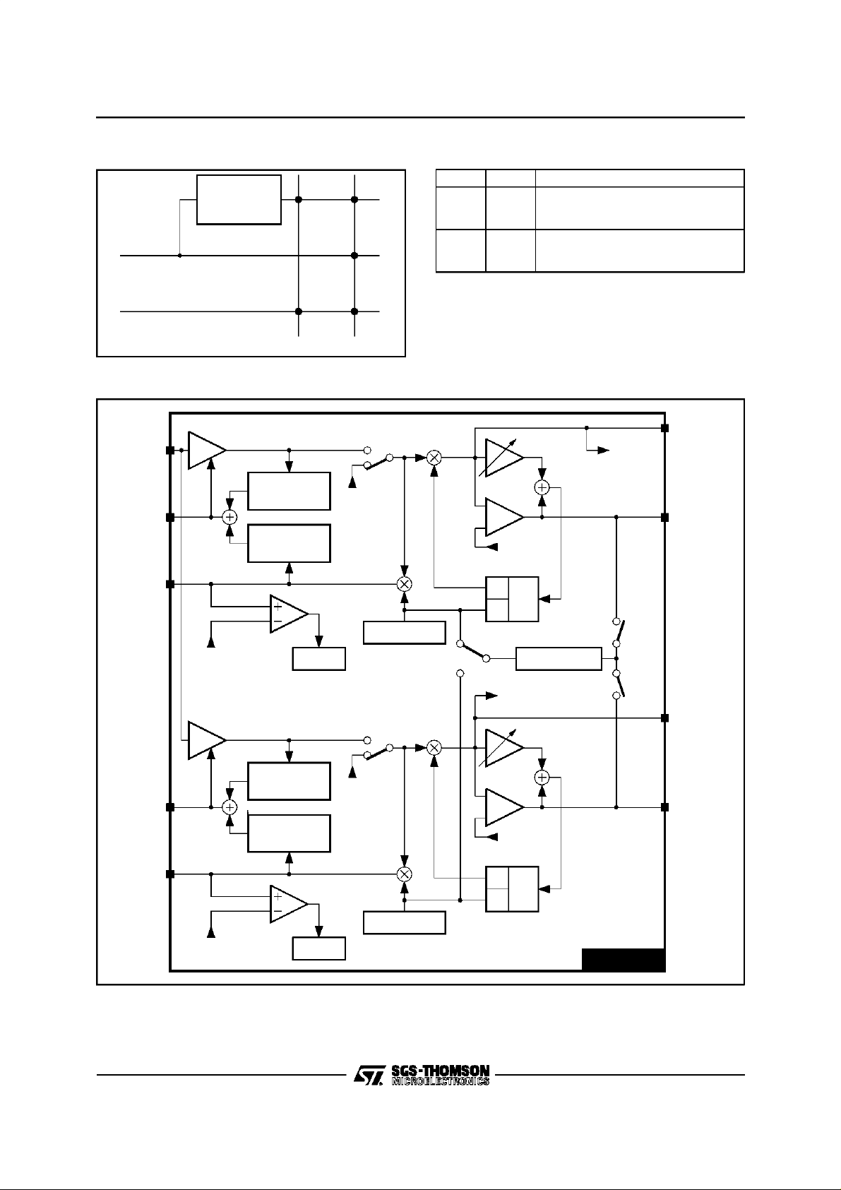
AUDIO SWITCHING
DEEMPHASIS
AUDIO PLL
AUDIO
+ ANRS
STV0042A
K
1a
K
5b
K
a
b
b
K
5c
a
b
b
K
2
1
2
1
2
ON
ON
ON
OFF
OFF
OFF
3
No ANRS, No De-emphasis
No ANRS, 50µs
No ANRS, 75µs
ANRS, No De-emphasis
ANRS, 50µs
ANRS, 75µs
AUX IN
K
1c
VOL OUT AUX OUT
FMDEMODULATION BLOCK DIAGRAM
FM IN
AGC R
AMPLKR
AGC
V
AGC
REF
LEVEL
DETECTOR1
LEVEL
DETECTOR2
Reg8 b4
Bias
Amp. Detect
K
5a
SW1
WATCHDOG
SW3
0042A-06.EPS
Phase
Detect
Phase
Detect
FM dev.
Select.
V
REF
90
VCO
0
SYNTHESIZER
AUDIOL
DETR
AUDIOR
CPUMP R
SW2
SW4
DETL
AGC L
AMPLKL
LEVEL
DETECTOR1
Bias
FM dev.
Select.
CPUMP L
LEVEL
DETECTOR2
V
REF
Amp. Detect
90
VCO
0
WATCHDOG
V
REF
Reg8 b0
STV0042A
0042A-07.EPS
7/24
Page 8

STV0042A
CIRCUITDESCRIPTION
1 - VideoSection
Thecompositevideo is first set to a standard level
by means of a 64 step gain controlledamplifier. In
thecasethat themodulationisnegative,an inverter
canbe switchedin.
One of two different external video de-emphasis
networks (for instance PAL and NTSC) is selectable by an integrated bus controlledswitch.
Then energy dispersal is removed by a sync tip
clamping circuit, which is used on all inputs to a
video switching matrix, thus making sure that no
DC steps occur when switching video sources.
The matrix can be used to feedvideo to and from
decoders,VCR’sand TV’s.
Additionaly all the video outputs are tristate type
(high impedance mode is supported), allowing a
simple parallel connections to the scarts (Twin
tunerapplications).
2 - Audio Section
Thetwoaudio channelsare totallyindependentexceptfor thepossibilitygivento outputonbothchannelsonlyone of the selectedinputaudiochannels.
To allow a very cost effective application, each
channel uses PLL demodulation. Neither external
complexfilter nor ceramicfiltersare needed.
The frequency of the demodulated subcarrier is
chosenby a frequencysynthesizerwhich sets the
frequency of the internal local oscillator by comparing its phase with the internally generated
reference. When the frequency is reached, the
microprocessor switches in the PLL and the demodulationstarts.Atanymomentthe microprocessor can read fromthe device(watchdog registers)
the actual frequencyto which the PLLis locked.It
canalsoverifythatacarrierispresentatthe wanted
frequency(by reading AMPLKstatus bit)thanks to
a synchronous amplitude detector, which is also
usedfor the audio input AGC.
In order to maintain constant amplitude of the
recovered audio regardless of variationsbetween
satellitesor subcarriers,the PLLloop gain may be
programmedfrom 56 values.
Any frequency deviation can be accomodated
(from ±30kHztill ±400kHz).
In thetypical application,theSTV0042Aofferstwo
audiode-emphasis75µsand 50µs. Whenrequired
a J17 de-emphasis can be implemented by using
specificapplicationdiagram(seeApplicationNote:
AN838, Chapter 4.2).
Adynamic noise reduction system (ANRS) is integrated into the STV0042A using a lowpass filter,
the cut-off frequency of which is controlled by the
amplitude of the audio after insertion of a bandpass filter.
Twotypes of audio outputs are provided: one is a
fixed 1V
2V
RMS
and the other is a gain controlled
RMS
max. The control range being from +12dB
to-26.75dBwith1.25dBsteps.Thisoutputcanalso
be muted.
A matrixis implementedto feed audioto and from
decodersVCR’s and TV’s.
Noise reduction system and de-emphasis can be
insertedor by-passedthroughbus control.
Also all the audio outputs are tristate-type (high
impedancemodeis supported),allowinga simple
parallel connections to the scarts (Twin tuner
applications).
3 - Others
A22kHz tone is generatedfor LNB control.
It isselectableby bus controland availableon one
of the two pins connected to the external video
de-emphasisnetworks.
By means of the I
2
C bus there is the possibility to
drive the ICs into a low power consumption mode
with a ctive audio and video matrixes. Independantly from the main power mode, each individualaudioand video outputcan bedrivento high
impedancemode.
8/24
Page 9

STV0042A
ABSOLUTE MAXIMUMRATINGS
Symbol Parameter Value Unit
V
CC
V
DD
P
tot
T
oper
T
stg
THERMAL DATA
Symbol Parameter Value Unit
Rth(j-a) Thermal Resistance Junction-ambient 60
DCAND AC ELECTRICAL CHARACTERISTICS
= 12V,VDD=5V,T
(V
CC
Symbol Parameter Test Conditions Min. Typ. Max. Unit
V
CC
V
DD
IQ
CC
IQ
DD
IQLP
CC
IQLP
DD
AUDIO DEMODULATOR
FMIN FM Subcarrier Input Level
DETH Detector1 and 2 (AMPLOCK Pins)
VCOMI VCO Mini Frequency V
VCOMA VCO Maxi Frequency 10 MHz
AP50 1kHz AudioLevel at PLL output
APA50 1kHz AudioLevel at PLL output
FMBW FM Demodulator Bandwidth Gain at 12kHz versus 1kHz
DPCO Digital Phase Comparator OutputCurrent
AUTOMATIC NOISE REDUCTION SYSTEM
LRS Output Level (Pin SUMOUT) 1V
LDOR Level Detector OutputResistance
NDFT Level Detector Fall Time Constant
NDLL Bias Level (Pins PK OUT) No audio in 2.40 V
LLCF Noise Reduction Cut-off Frequency at
HLCF Noise Reduction Cut-off Frequency at
Supply Voltage 15
7.0
Total Power Dissipation 900 mW
Operating Ambient Temperature 0, + 70
Storage Temperature -55, + 150
=25oC unless otherwise specified)
amb
Sypply Voltage 11.4
4.75125.0
Supply Current All audio and all video outputs
12.6
5.25VV
5587015mA
activated
Supply Current at Low Power Mode All audio and all video outputs
276359mA
are in highimpedance mode
(Pin FMIN for AGC action)
VCO locked on carrier at 6MHz
560kΩ load on AMPLOCK Pins
5 500 mV
180kΩ load on DET Pins
(Threshold for activating Level Detector 2)
(DET Pins)
(DET Pins)
8mV
Carrier without modulation
CC
T
amb
0.5V
Coarse deviation set to 50kHz
(Reg. 05 = 36
FMIN≤500mV
≤
PP
: 11.4 to 12.6V,
: 0 to 70oC
50kHz dev. FM input,
PP
)
HEX
PP
0.5VPP50kHz dev. FM input,
Coarse and fine settings used
2.90 3.10 3.30 V
5 MHz
0.6 1 1.35 V
0.92 1 1.08 V
0 0.3 1 dB
180kΩ, 82kΩ22pF on DET Pins
(CPUMP Pins)
Average sink andsource
current to externalcapacitor
on left and right channel 0.9 1 1.1 V
PP
60 µA
4.0 5.4 6.8 kΩ
(Pins PK OUT)
(Pins PK OUT)
Low Level Audio
High Level Audio
External 22nF toGND and
1.2MΩ to V
100mV
capacitor 330pF (FC Pins)
1V
PP
capacitor 330pF (FC Pins)
REF
on DET Pins,External
PP
on DET Pins,External
26.4 ms
0.85 kHz
7 kHz
o
C/W
V
V
o
o
mA
mA
C
C
0042A-02.TBL
0042A-03.TBL
PP
PP
PP
PP
0042A-04.TBL
9/24
Page 10

STV0042A
DCAND AC ELECTRICAL CHARACTERISTICS (continued)
= 12V,VDD=5V,T
(V
CC
Symbol Parameter Test Conditions Min. Typ. Max. Unit
AUDIO OUTPUT (Pins VOL OUT R, VOL OUT L)
DCOL DC OutputLevel 4.8 V
AOLN AudioOutput Level
with Reg 00 = 1A
AOL50 Audio Output Level
with Reg 00 = 1A
AOL75 Audio Output Level
with Reg 00 = 1A
AMA1 Audio Output Attenuation
with Mute-on. Reg 00 = 00.
MXAT Max Attenuationbefore Mute.
Reg 00 = 01.
MXAG Audio Gain. Reg 00 = 1F. 1kHz, from S2 RTN Pins 5 6 7 dB
ASTP Attenuation of each of the 31 steps 1kHz 1.25 dB
THDA1 THD with Reg 00 = 1A 1V
THDA2 THD with Reg 00 = 1A 2V
THDFM THD with Reg 00 = 1A FM inputas for APA50
ACS Audio Channel Separation 1V
ACSFM Audio Channel Separation at 1kHz - 0.5 V
SNFM Signal to Noise Ratio FM input as for APA50,
SNFMNR Signal to Noise Ratio FM inputas for APA50
Z
OUT L
Z
OUT H
Audio Output Impedance Low impedance mode
AUXILIARY AUDIO OUTPUT (Pins S2 OUT R, S2 OUT L)
DCOLAO DC output level Aux. input pins open circuit 4.8 V
AOLNS Audio Output Levelon S2 FM input as for APA50
AOL50S Audio Output Levelon S2 FM inputas for APA50
AOL75S Audio Output Levelon S2 FM inputas for APA50
THDAOFM THD on S2 FM input as for APA50
Z
OUT L
Z
OUT H
Audio Output Impedance Low impedance mode
=25oC unless otherwise specified)
amb
FM input as for APA50
No de-emphasis, No pre-emphasis
No noise reduction
FM input as for APA50
50µs de-emphasis, 27kΩ//2.7nF load
No pre-emphasis, No noise reduction
FM input as for APA50
75µs de-emphasis, 27kΩ//2.7nF load
No pre-emphasis, No noise reduction
1VPP- 1kHz from S2 RTN Pins 60 65 dB
1kHz, from S2 RTN Pins 32.75 dB
-1kHz from S2 RTN Pins 0.15 %
PP
-1kHz from S2 RTN Pins 0.3 1 %
PP
75µs de-emphasis, ANRS ON
-1kHz on S2 RTN Pins 60 74 dB
PP
- 50kHz deviation FM inputon
PP
one channel
- 0.5V
no deviation FM inputon the
PP
other channel
- Reg 05 = 36
-75µs de-emphasis, no ANRS
75µs de-emphasis,
no ANRS, Unweighted
75µs de-emphasis,
ANRS ON, Unweighted
High impedance mode 301844 55ΩkΩ
No de-emphasis, No pre-emphasis
No noise reduction
50µs de-emphasis, 27kΩ//2.7nF load
No pre-emphasis, No noise reduction
75µs de-emphasis, 27kΩ//2.7nF load
No pre-emphasis, No noise reduction
75µs de-emphasis, no ANRS
High impedance mode 306044
1.5 1.9 2.34 V
2.0 3.3 4.0 V
2.0 3.3 4.0 V
0.3 1 %
60 dB
HEX
56 dB
69 dB
1.55 2 2.42 V
2.0 3.4 4.0 V
2.0 3.4 4.0 V
0.3 1 %
10055Ω
kΩ
PP
PP
PP
PP
PP
PP
0042A-05.TBL
10/24
Page 11

STV0042A
DCAND AC ELECTRICAL CHARACTERISTICS (continued)
= 12V,VDD=5V,T
(V
CC
Symbol Parameter Test Conditions Min. Typ. Max. Unit
RESET
RTCCU End of Reset Threshold for V
RTCCD Start of Reset Threshold for V
RTDDU End of Reset Threshold for V
RTDDD Start of Reset Threshold for V
COMPOSITE SIGNAL PROCESSING
VIDC VID IN External load current < 1µA 2.25 2.45 2.65 V
ZVI VID IN Input Impedance 7 11 14 kΩ
DEODC DC Output Level (PinsVIDEEM) 2.25 2.45 2.65 V
DEOMX Max AC Level before Clipping
(Pins VIDEEM)
DGV Gain error vs GV @ 100kHz GV= 0 to 12.7dB, Reg 01 = 00 → 3F -0.5 0 0.5 dB
INVG Inverter Gain -0.9 -1 -1.1
VISOG Video Input to SCART Output Gain De-emphasis amplifier mounted in unity
DEBW Bandwidth for 1V
measured on Pins VIDEEM
DFG Differential Gain on Sync Pulses
measured on Pins VIDEEM
ITMOD Intermodulation of FM subcarriers
with chroma subcarrier
CLAMP STAGES (Pins CLAMP IN, S2)
ISKC Clamp Input Sink Current V
ISCC Clamp Input Source Current V
VIDEO MATRIX
XTK Output Level on any Outputwhen
CVBS input is selectedfor
1V
PP
any other output
BFG OutputBufferGain
(PinsS1 VIDOUT,S2 VID OUT)
DCOLVH DC Output Level High impedance mode 0 0.2 V
Z
OUT HV
Video Output Impedance High impedance mode 16 23 30 kΩ
VCL Sync TipLevel on SelectedOutputs
(Pins S1 VID OUT, S2 VID OUT)
=25oC unless otherwise specified)
amb
CC
DD
VDD= 5V, VCCgoing up 8.7 V
VDD= 5V, VCCgoing down 7.9 V
CC
VCC= 12V, VDDgoing up 3.8 V
VCC= 12V, VDDgoing down 3.5 V
DD
GV = 0dB, Reg 01 = 00 2 V
gain, Normal video selected
PP
input
@ - 3dB with GV = 0dB, Reg 01 = 00 10 MHz
GV = 0dB, 1V
25Hz sawtooth (input : VID IN)
7.02 and 7.2MHz sub-carriers,
12.2dB lower than chroma
= 3V 0.5 1 1.5 µA
IN
=2V 40 50 60 µA
IN
@ 5MHz -60 dB
@ 100kHz 1.87 2 2.13
CVBS through 10nF on input 1.05 1.3 1.55 V
1V
PP
CVBS + 0.5V
PP
PP
-1 0 1 dB
1%
-60 dB
PP
0042A-06.TBL
11/24
Page 12

STV0042A
PIN INTERNAL CIRCUITRY
S2 VID RTN, CLAMPIN
50µAsource is activeonly when VIDIN < 2.7V.
Figure 1
V
9V
DD
50µA
10k
4
60
2.3mA
Ω
Ω
1µA
60Ω
GND 0V
1
1
V
5V
DD
GND0V
V
12V
CC
S1 VID OUT
S2 VID OUT
20kΩ
20kΩ
GND 0V
V
12V
CC
V
2.4V
REF
S2 VID RTN
CLAMPIN
S1 VID OUT, S2 VID OUT
Sameas abovebut withno black level adjustment.
Figure3
VID MUX 10kΩ
UNCLDEEM
Sameas above but withno black level adjustment
and slightly differentgain.
Figure4
VIDEEM1
Ron of the transistorgate is≈10kΩ.
Figure 5
6µ/2µ
10µ/2µ
VIDEEM1
VIDEEM2/ 22kHz
Ron of the transistorgate is ≈10kΩ.
Figure 6
0042A-08.EPS
6µ/2µ
10µ/2µ
VIDEEM2/22kHz
V
100µ/2µ
60µ/2µ
VID IN
Figure7
0042A-09.EPS
VID IN
V
REF
10kΩ
6.5k
2.4V
Ω
0.5pF
GND 0V
1
125µA
0042A-11.EPS
1
125µA
5V
DD
22kHz
0042A-12.EPS
1
+
85µA
0042A-13.EPS
4
IN 10k
2.3mA
GND 0V
12/24
Ω
25k
16.7kΩ
GND 0V
Ω
UNCL DEEM
V
2.4V
REF
PK OUT
Figure 8
Audio
0042A-10.EPS
Peak Detector
VDD9V
1
Clamp
3.4V
1
5kΩ
PK OUT
0042A-14.EPS
Page 13

PIN INTERNAL CIRCUITRY(continued)
FC L, FC R
Ivar is controlled by the peak det audio level max.
±15µA(1V
PP
audio).
Figure9
STV0042A
FM IN
Theotherinputfor eachchannelis internallybiased
in the same way via 10kΩ to the2.4V V
Figure 13
REF
.
VDD9V
FC L
FC R
Ivar
1
1
VOLOUT R, VOL OUT L
Audio output with volume and scart driver with
+12dB of gain for up to 2V
. The opamp has a
RMS
push-pulloutputstage.
Figure10
Audio
2.4V Bias
30kΩ
15kΩ
30kΩ
GND 0V
4.8V
VOL OUT R
VOL OUT L
S2 OUT L, S2 OUT R
Sameas above but withgain fixed at +6dB.
Figure11
Audio
2.4V Bias
20kΩ
S2 OUT L
S2 OUT R
FM IN
0042A-15.EPS
I
REF
2.4V
The optimum value if I
Ω
Ω
10k
RightChannel
REF
1
is 50µA±2% so an
Left Channel
1
50µA
50µA
10k
external resistorof 47.5kΩ ±1% is required.
Figure 14
2.4V
1
I
REF
SCL
Thisis theinput toa Schmittinput buffermade with
a CMOSamplifier.
Figure 15
0042A-16.EPS
SCL 24µ/4µ
205
ESD
Ω
SDA
Inputsameasabove.Outputpulldown only: relies
on external resistor for pull-up.
Figure 16
0042A-19.EPS
0042A-20.EPS
0042A-21.EPS
20kΩ
GND 0V
S2 RTN L, S2 RTN R
4.8V bias voltageis thesame as the bias level on
the audio outputs.
Figure12
25kΩ
S2 RTN L
S2 RTN R
4.8V
1
50µA
SDA
600µ/2µ
0042A-17.EPS
205Ω
24µ/4µ
ESD
GND0V
U75 L, U75 R
I1 - I2= 2 x audio/ 18kΩ.eg1VPPaudio: ±55µA.
The are internal switches to matchthe audio level
of the differentstandards.
Figure 17
I1
U75 L
U75 R
0042A-18.EPS
I2
0042A-22.EPS
0042A-23.EPS
13/24
Page 14

STV0042A
PIN INTERNAL CIRCUITRY(continued)
XTL
Figure18
460
5pF
GND 0V
XTL
750µA
460
Ω
232
500µA
CPUMPL, CPUMPR
Anoffset on the PLL loop filter will causean offset
in the two 1µA currents that will prevent the PLL
fromdrifting-offfrequency.
Figure19
100µA
Dig Synth
CPUMP L
CPUMP R
100µA
1µA
Loop Filter Tracking
1µA
VCO Input
DET L, DETR
I2 - I1 = f (phaseerror).
Figure20
I2
DET L
DET R
I1
AMPLKL, AMPLK R, AGC L, AGCR
I2 and I1 from the amplitudedetectingmixer.
Figure21
To VCA
AMPLK L
AMPLKR
I2
2
I1
10k
Ω
V
2.4V
REF
5µA
160µA
3
Ω
750µA
AGC L
AGC R
V
REF
The 400µA source is off during stand-by mode.
Figure22
V
Vbg 1.2V
0042A-24.EPS
4
10kΩ
10kΩ
GND 0V
REF
400µA
SUMOUT
Figure 23
2.4V
V
REF
1
Audio
49k
50k
Ω49kΩ
Ω
100µA
PK IN
Figure 24
V
2.4V
0042A-25.EPS
PK IN
REF
67k
1
To Peak Det
Ω
100µA
V 12V
Doubledbonded (two bond wires and twopadsfor
one package pin) :
0042A-26.EPS
- One pad is connectedto all of the 12V ESD and
video guard rings.
- The second pad is connected to power up the
video block.
V GND
Doubledbonded :
- Onepadisconnectedtopower-upall ofthevideo
mux and I/O.
- The second pad is only as a low noise GND for
the video input.
VDD5V,GND 5V
Connected to XTL oscillator and the bulk of the
0042A-27.EPS
CMOS logicand 5V ESD.
(2.4V)
0042A-28.EPS
SUMOUT
0042A-29.EPS
0042A-30.EPS
14/24
Page 15

PIN INTERNAL CIRCUITRY(continued)
A GND L
Doubledbonded :
- One pad connected to the left VCO, dividers,
mixers and guard ring. the guard connection is
star connected directly to the pad.
- The secondpadis connectedto bothAGC amps
and the deemphasis amplifiers, frequency synthesis and FM deviation selection circuit for both
channels.
A 12V
Doubledbonded :
- One pad connectedto theESD and guard ring.
- The secondpad is connectedto themain power
for all of the audioparts.
A GND R
Boubledbonded:
- One pad connected to the right VCO, dividers,
mixers and guard ring. The guard connectionis
star connected directly to the pad.
- The second pad is connected to the bias block,
audio noise reduction,volume, mux and ESD.
STV0042A
A third bond wire on this pin is connected directly
to the die pad (substrate).
Figure 25
V 12V
VideoPads
V GND
VDD5V
Vpp
BIP 10vpl
Vmm
Substrate
DigitalPads
GND5V
A GND L
A 12V
AudioPads
A GND R
205Ω
BIP
12V
DZPN1
DZPN1
DZPN1
+
-
0042A-31.EPS
15/24
Page 16

STV0042A
I2C PROTOCOL
1) WRITING to the chip
S-StartCondition
P-Stop Condition
CHIPADDR - 7 bits. 06H
W-Write/Read bit is the 8th bit of thechip address.
A-ACKNOWLEDGEafter receiving8 bits of data/adress.
REGADDR Address of register to be written to, 8 bitsof which bits3, 4, 5, 6 & 7 are ’X’ or
don’t care ie
DATA 8 bits of databeingwrittento the register.All8 bitsmustbe writtento atthesame
time.
REGADDR/A/DATA/A can be repeated,the write process can continue untill terminatedwith a STOP
condition.If the REG ADDR is higher than 07 then IIC PROTOCOL will stillbe
met (ie an A generated).
Example:
S06WA00A55A01A8F A P
2) READING from the chip
Whenreading,thereis anauto-incrementfeature. Thismeansanyreadcommandalwaysstartsby reading
Reg 8 andwill continue to read the following registers in order after each acknowledge or untilthere is no
acknowledge or a stop. This function is cyclic that is it will read the same set of registers without
re-addressingthe chip. There are two modes of operationas set by writing to bit 7 of register 0. Read 3
registersin a cyclic fashionor all5 registersin acyclic fashion. Note only the last 5 of the11 registerscan
be read.
Reg0 bit 7 = L ⇒ Start/ chip add / R /A/ Reg 8 / A/ Reg9 / A/ Reg 0A/ A/ Reg8 / A/ Reg 9 / A/ Reg0A
/... / P /
Reg0 bit 7 = H⇒ Start/ chipadd / R / A / Reg 8 / A/ Reg 9 / A/ Reg 0A / A/ Reg 7 / A/ Reg 6/ A / Reg 8
/ A/ Reg9 / A/ Reg 0A/ A / Reg 7 /A / Reg 6 / ... / P /
only the first 3 bitsare used
.
CONTROL REGISTERS
Reg 0 writeonly
Bit (default 00
HEX
)
0 L Select 5 bits audio volumecontrol 00H = MUTE
1 L Select 5 bits audio volumecontrol 01H = -26.75dB
2 L Select 5 bits audio volumecontrol : : : : :
3 L Select 5 bits audio volumecontrol 1.25dB steps up to
4 L Select 5 bits audio volumecontrol 1FH = +12dB
5 L Not to be used
6 L Audio mux switch K3 - ANRSselect (L = no ANRS, H = ANRS)
7 L L = read 3 registers,H = read 5 registers
Reg 1 writeonly
Bit (default 00
HEX
)
0 L Select video gain bits
1 L Select video gain bits 00H = 0dB
2 L Select video gain bits 01H = +0.202dB
3 L Select video gain bits 02H = +0.404dB
4 L Select video gain bits n = + 0.202 dB * n
5 L Select video gain bits 3FH = + 12.73dB
6 L Selectedvideo invert (H = inverted,L= non inverted)
7 L Videodeemphasis1 / Videodeemphasis2 (L: V
16/24
De-em1)
ID
Page 17

CONTROL REGISTERS(continued)
Reg 2 writeonly
Bit (default F7
HEX
)
0 H Select video sourcefor scart1 O/P
1 H Select video sourcefor scart1 O/P
2 H Select video sourcefor scart1 O/P
3 L Select 4.000MHzor 8.000MHzclock speed (L = 8MHz)
4 H Select audio source for volume output (Switch K1)
5 H Select audio source for volume output (Switch K1)
6 H Select Left/Right/Stereofor volumeoutput
7 H Select Left/Right/Stereofor volumeoutput
Reg 3 writeonly
Bit (default F7
HEX
)
0 H Select video sourcefor scart2 O/P
1 H Select video sourcefor scart2 O/P
2 H Select video sourcefor scart2 O/P
3 L Videodeemphais2 / 22kHz(H : 22kHz)
4 H Select audio source for Scart 2 output (Switch K5)
5 H Select audio source for Scart 2 output (Switch K5)
6 H Audio deemphasisselect (Switch K2)
7 H Audio deemphasisselect (Switch K2)
STV0042A
Reg 4 writeonly
Bit (default BF
HEX
)
0 H Not to be used
1 H Not to be used
2 H Not to be used
3 H Stand-by or low power mode (H = low power)
4 H Not to be used
5 H Not to be used
6 L Not to be used
7 H Not to be used
Reg 5 writeonly
Bit (default B5
HEX
)
0 H FM deviationselection-- defaultvalue for 50kHz modulation
1 L FM deviation selection
2 H FM deviationselection
3 L FM deviation selection
4 H FM deviationselection
5 H FM deviationselection(L = double the FM deviation)
6 L Not to be used
7 H Not to be used
Reg 6 write/read
Bit (default 86
HEX
)
0 L Statusof I/O
1 H Select data direction of I/O 1 ( H = output)
2 H Select frequency synthesizer1 OFF/ON(L = OFF)
3 L Select frequencysynthesizer2 OFF/ON(L= OFF)
4 L Select RF source(L = OFF) to FM det 1
5 L Select RF source(L = OFF) to FM det 2
6 L Select frequencyfor PLL synthesizer- LSB (bit 0) of 10-bit value
7 H Select frequency for PLL synthesizer- bit1 of 10-bitvalue
17/24
Page 18

STV0042A
CONTROL REGISTERS(continued)
Reg 7 write/read
Bit (default AF
0 H Select frequency for PLL synthesizer- bit2 of 10-bitvalue
1 H Select frequency for PLL synthesizer
2 H Select frequency for PLL synthesizer
3 H Select frequency for PLL synthesizer
4 L Select frequencyfor PLL synthesizer
5 H Select frequency for PLL synthesizer
6 L Select frequencyfor PLL synthesizer
7 H Select frequency for PLL synthesizer- bit9, MSB(10th bit) of 10-bit value
Reg 8 read only
Bit
0 Subcarrierdetection (DET 1) (L = Nosubcarrier)
1 Not used
2 Read frequencyof watchdog 1 - LSB (bit 0) of 10-bit value
3 Read frequencyof watchdog 1 - bit 1 of 10-bitvalue
4 Subcarrierdetection (DET 2) (L = Nosubcarrier)
5 Not used
6 Read frequencyof watchdog 2 - bit 0 of 10-bitvalue
7 Read frequencyof watchdog 2 - bit 1 of 10-bitvalue
HEX
)
Reg 9 read only
Bit (default AF
HEX
)
0 Read frequencyof watchdog 1 - bit 2 of 10-bitvalue
1 Read frequencyof watchdog 1
2 Read frequencyof watchdog 1
3 Read frequencyof watchdog 1
4 Read frequencyof watchdog 1
5 Read frequencyof watchdog 1
6 Read frequencyof watchdog 1
7 Read frequencyof watchdog 1 - bit 9, MSB(10th bit) of 10-bit
Reg 0A read only
Bit
0 Read frequencyof watchdog 2 - bit 2 of 10-bitvalue
1 Read frequencyof watchdog 2
2 Read frequencyof watchdog 2
3 Read frequencyof watchdog 2
4 Read frequencyof watchdog 2
5 Read frequencyof watchdog 2
6 Read frequencyof watchdog 2
7 Read frequencyof watchdog 2 - bit 9, MSB(10th bit) of 10-bit
18/24
Page 19

CONTROL REGISTERS(continued)
VideoMux Truth Tables
Register2 <0:2>⇒Scart1 video output control
Register3 <0:2> ⇒ Scart2 video output control
Thetruth table for the three scartoutputs are the same.
Register 2/3 Video Output
Bit<2>
0
0
0
0
1
1
1
1
Bit<1>
0
0
1
1
0
0
1
1
Bit<0>
0
1
0
1
0
1
0
1
Baseband video
De-emphasized video
Normal video
Not to be used
Scart 2 return
Not to be used
Nothing selected
High Z or low power (default)
AudioMux TruthTables
Register 2 Switch K1/Audio Source Selection for Volume Output
Bit <5>
0
1
0
1
Bit <4>
0
0
1
1
Volume Output
A
Audio deemphasis (K2 switch O/P)
C
Scart 2 return
B
Not to be used
-
High Z or low power (default)
STV0042A
Register 3 Switch K2/Audio Deemphasis
Bit <7>
0
1
0
1
Bit <6>
0
1
X
X
Bit <5>
0
1
0
1
Register 2 Left / Right / Stereo on Volume Output
Bit <7>
0
1
1
Bit <6>
0
0
1
1
Register 0 Switch K3 & K4
Bit <5>
X
X
0
1
Register 3 Switch K5/Audio Source Selection for Scart 2
Bit <4>
0
0
1
1
Bit <6>
0
0
1
Mono left /channel 1
Mono right / channel 2
Stereo left & right (default)
Audio Deemphasis
A
No deemphasis
C
Not to be used
B
50µs
B
75µs (default)
ANRS I/O Select
A
Noise reduction OFF
B
Noise reduction ON (default)
A
Not to be used
B
Not to be used
Aux Audio Output
C
PLL output
A
Not to be used
B
Audio deemphasis (K2 switch O/P)
-
High Z or low power state (default)
19/24
Page 20

STV0042A
CONTROL REGISTERS(continued)
Register5 : FM DeviationSelection
43210
0
0
0
0
0
0
0
0
0
0
0
0
0
0
0
0
1
1
1
1
1
1
1
1
1
1
1
1
1
1
1
1
Example : Default power up state54.4kHz ⇒±54.4kHz.
0
0
0
0
0
0
0
0
1
1
1
1
1
1
1
1
0
0
0
0
0
0
0
0
1
1
1
1
1
1
1
1
0
0
0
0
1
1
1
1
0
0
0
0
1
1
1
1
0
0
0
0
1
1
1
1
0
0
0
0
1
1
1
1
0
0
1
1
0
0
1
1
0
0
1
1
0
0
1
1
0
0
1
1
0
0
1
1
0
0
1
1
0
0
1
1
0
1
0
1
0
1
0
1
0
1
0
1
0
1
0
1
0
1
0
1
0
1
0
1
0
1
0
1
0
1
0
1
Selected Nominal Carrier Modulation
Bit 5 = 0 Bit 5 = 1
Do not use
Do not use
Do not use
Cal. set. (2V)
592kHz
534kHz
484kHz
436kHz
396kHz
358kHz
322kHz
292kHz
266kHz
240kHz
218kHz
196kHz
179kHz
161kHz
146kHz
122kHz
120kHz
109kHz
98kHz
89kHz
78kHz
71kHz
65kHz
58kHz
53kHz
48.6kHz
43.8kHz
39.6kHz
cal : do not use = 0.3373V offseton VCO
cal : do not use = 0.3053V offseton VCO
cal : do not use = 0.2763V offseton VCO
calibration setting (1V offset on VCO)
296kHz modulation
267kHz modulation
242kHz
218kHz
198kHz
179kHz
161kHz
146kHz
133kHz
120kHz
109kHz
98.3kHz
89.7kHz
80.9kHz
73.1kHz
66.0kHz
60.0kHz
54.4kHz = default power up state
49.1kHz
44.3kHz
39.8kHz
35.9kHz
32.4kHz
29.1kHz
26.7kHz
24.3kHz
21.9kHz
19.7kHz
Register 1
Bit <7>
0
0
1
1
Register 3
Bit <3>
0
1
0
1
Deemphasis 1 (default)
Deemphasis 1 + 22kHz (Pin 13)
Deemphasis 2
Deemphasis 2
FMDEMODULATION SOFTWARE ROUTINE
WiththeSTV0042Acircuit,foreachchannel,three
stepsarerequired to acheivea FMdemodulation:
st
step:To set the demodulationparameters :
-1
• FM deviationselection,
• Subcarrier frequencyselection.
nd
-2
step : To implement a waiting loop to check
the actual VCO frequency.
rd
-3
step:To close the demodulationphaselocked
loop (PLL).
Refering to the FM demodulation block diagram
(page 12), the frequency synthesis block is commonto bothchannels(leftand right); consequently
20/24
Video Deemphasis/22kHz
twocompletesequenceshaveto bedoneone after
the other when demodulatingstereopairs.
Detailed Description
Conventions:
- R = Stands for Register
- B = Standsfor Bit
Example :
R05 B2 = Register 05, Bit 2
For clarity, the explanationsare basedon the following example : stereo pair 7.02MHz/L
7.20MHz/R,deviation±50kHz max.
Page 21

FMDEMODULATION SOFTWARE ROUTINE(continued)
1stStep(Left):SettingtheDemo dulati onParam eters
A. The FMdeviationis selectedby loadingR5 with
the appropriatevalue. (seeR5 truth table).
NB : Verywide deviations (up to ±592kHz)can be
accomodatedwhen R5 B5 is low.
Corresponding bandwidth can be calculated as
follows:
Bw ≈ 2 (FM deviation + audio bandwidth)
Bw≈2 (valuegiven in table + audiobandwidth)
In the example:
R5Bits 76543210
XX110110
B. Thesubcarrierfrequencyisselectedby launching
afrequencysynt hesis(theVCOisdriventothewanted
frequency ) .This operationrequirestwo actions:
- To connect the VCO to the frequency synthesis
loop.Referingtothe FM blockdiagram(page12):
•
SW4 closed
⇒
R6 B2 = H
• SW3 to bias ⇒ R6 B4= L
• SW2 to bias
⇒ R6 B3 = L
• SW1 opened ⇒ R6B5 = L
- To load R7 and R6 B6 B7 with the value corresponding to the left channel frequency. This 10
bits value is calculatedas follows:
Subcarrierfrequency = codedvalue x 10kHz
(10kHz is the minimum step of the frequency
synthesisfunction). Consideringthatthe tunning
range is comprised between 5 to 10MHz, the
coded value is a numberbetween 500 and 1000
10
= 1024) then 10 bits are required.
(2
the watchdog.
3rdStep (Left)
TheFMdemodulationcanbestartedbyconnecting
the VCO to the phase locked loop (PLL).
In practice:
- SW3 closed⇒R6 B4 = H
- SW4 opened ⇒ R6 B2 = L
After this sequence of 3 steps for left channel,
a similarsequenceis needed for the rightchannel.
Note :
Inthesequencefortheright,thereisnoneedtoagain
selecttheFMdeviation(onceisenoughforthepair).
GeneralRemark
Before to enable the demodulated signal to the
audiooutput, it isrecommandedto keepthemuting
and to checkwhethera subcarrieris presentat the
wantedfrequency.Suchan informationisavailable
in R8 B0 andR8 B4which can be read.
Twodifferentstrategiescan be adoptedwhenenabling the output :
- Eitherbothleftandrightdemodulatedsignalsaresimul taneouslyauthorizedwhenbothchannelareready.
- Or while the rightchannelsequenceis running,the
alreadyready left signal is sent to the leftand right
outputsandtherealstereosoundL/Risoutputwhen
bothchannelsare ready. This secondoption gives
sounda fewhundredsof msbeforethefirstone.
Table1: FrequencySynthesisRegisterSettingfor
the Most Common SubcarrierFrequencies
Example :
7.02MHz= 702x 10kHz
702⇒1010 1111 10
⇒
AF + 10
Subcarrier Freq. (MHz)
R7 is loaded with AF and R6 B6 : L, R6 B7 : H.
TheTable1 givesthesettingfor themostcommon
subcarrierfrequencies.
2ndStep(Left) : VCOFrequencyChecking(VCO)
Thissecondstepisactuallyawaitingloopinwhichthe
actualrunningfrequencyoftheVCOis measured.
To exit of this loop is allowed when : Subcarrier
Frequency- 10kHz≤MeasuredFrequency≤SubcarrierFrequency+10kHz(± 10kHzisthemaximum
dispersionof the frequencysynthesisfunction).
Inpractice,R8B2B3andR9arereadandcompared
tothevalueloadedin R6 B6 B7 andR7 ±1 bit.
Note :
The duration of this step depends on how large is
frequencydifference between the start frequency
and the targetedfrequency.Typically:
- therate ofchangeof the VCOfrequencyis about
3.75MHz/s(C
pump
=10µF)
- In addition to this settling time, 100ms must be
added to takeintoaccountthe samplingperiod of
STV0042A
Register 7
(Hex)
5.58 8B 1 0
5.76 90 0 0
5.8 91 0 0
5.94 94 1 0
6.2 9B 0 0
6.3 9D 1 0
6.4 A0 0 0
6.48 A2 0 0
6.5 A2 1 0
6.6 A5 0 0
6.65 A6 0 1
6.8 AA 0 0
6.85 AB 0 1
7.02 AF 1 0
7.20 B4 0 0
7.25 B5 0 1
7.38 B8 1 0
7.56 BD 0 0
7.74 C1 1 0
7.85 C4 0 1
7.92 C6 0 0
8.2 CD 0 0
8.65 D8 0 1
Register 6
Bit 7 Bit 6
21/24
Page 22

STV0042A
TYPICALAPPLICATION (with 2 videodeemphasis network)
TV SCART
VCR/DECODERSCART
C4
R13, R12, C15, R14, C14 is shown
for 525 lines systems.
20
18
16
14
12
10
8
6
4
2
220nF
Ω
R6
75
20
18
16
14
12
10
8
6
4
2
J6RJ5
L
21 J1
19
17
15
13
11
9
7
5
3
1
21 J2
19
17
15
13
11
9
7
5
3
1
C5
2.2µF
C6
C8
2.2µF
2.2µF
C7
2.2µF
TDK FILTER
CCV
V
CCV
V
R5 68Ω
C11
8.2nF
SEL5618
Q1
Q2
3
2
1
BC547
BC547
V
R16
J4
C64
1.5nF
R2 68Ω
R3
470Ω
JP9
JP10
JP8
123456789101617181920 111213141521
C2
2.2µF
C3
2.2µF
R4
470Ω
R14 5.6kΩ
R13 10kΩ
R9 5.1kΩ
C14 150pF
C15
16V
10µF
+
R10 10kΩ
R12 1.8kΩ
Ω
1k
R15
JP11
C12 100pF
CCV
C23
C25
C26
8.2nF
R17 470Ω
100pF
J7
V
10µF
16V
JP1
L4
47µH
Ω
R18
1k
Ω
R48
75
+
C13
10µF 16V
R11 1.5kΩ
Ω
1k
R57
C56
C24
Ω
24k
C65
100nF
100nF
27pF
Ω
R54
3.3k
C62
C63
220nF
Ω
R58
43k
R59
1.2MΩ
C50
+
STV0042A
29 30 36 37 38 4031 32 33 34 35 39 41 4228272625242322
C41
+
JP2
123
1
1I/O
J10
J9
J8
INPUT
CLOCK
5V
8.2nF
JP5
10µF
CCA
V
C43
10µF
DD
V
SDA
16V
100nF
16V
JP6
C65
C66
SCL
JP7
C29
47pF
47pF
R50
4
GND
R55
R56
R53
R60
47.5kΩ
22pF
Ω
1.5k
Ω
10k
Ω
43k
Ω
1.2M
1%
R37
C45
C42
R36
560kΩ
560kΩ
4MHz or
J11
Q4
BC557
100nF
100nF
8MHz Crystal
DD
V
15V
+
C61
C60
C66
C58
C30
C31
L1 22µH
1.5nF
1.5nF
100nF
100nF
R51
100nF
220µF
1
GND
560kΩ
16V
J12
CCA
V
Ω
R41
82k
C48
22pF
C47
22pF
R40
180kΩ
C46
2.7nF
R39
27kΩ
C40
470µF
16V
+
R34
27kΩ
C39
2.7nF
R33
180kΩ
C38
22pF
Ω
R32
C37
22pF
82k
CCV
CCA
V
V
C32
100nF
C34
100nF
C33
220µF
C35
220µF
16V
J14
16V
+
+
1
112V
J13 L2 22µH
GND
22/24
Optionally : A second video deemphasis network
SEL5618 : 5MHz LPF made by TDK / Japan
INPUT
TUNER
0042A-32.EPS
Page 23

TYPICALAPPLICATION (with 22kHz tone and threeaudio de-emphasis50µs, 75µs, J17)
R54
TV SCART
C4
220nF
R59
3.3kΩ
C63
220nF
R58
43kΩ
1.2MΩ
J6RJ5
L
J1
21
20
19
18
17
16
15
14
13
12
11
10
9
8
7
6
5
4
3
2
1
J4
V
CCV
V
CCV
V
R5 68Ω
Q1
Q2
BC547
BC547
R2 68Ω
R3
470Ω
C2
2.2µF
C3
2.2µF
R4
470Ω
JP9
JP11
JP10
JP8
C64
123456789101617181920 111213141521
R57
1.5nF
C65
24kΩ
100nF
R55
1.5kΩ
C61
1.5nF
C62
8.2nF
Q4
BC557
R56
10kΩ
R53
43kΩ
JP5
R60
1.2MΩ
JP7
C58
100nF
47.5kΩ -1%
R51
R50
+
16V
C50
10µF
R37 560kΩ
CCA
V
C60
1.5nF
C66
100nF
C48
22pF
C47
560kΩ
R40
4.7kΩ
8.2nF
36kΩ
2.7nF
STV0042A
R41
82kΩ
22pF
180kΩ
75/J17
4.7kΩ
VCR/DECODER SCART
R13, R12, C15, R14, C14 is shown
Optionally : A second video deemphasis network
R6
75Ω
for 525 lines systems.
J2
21
20
19
18
17
16
15
14
13
12
11
10
9
8
7
6
5
4
3
2
1
SEL5618 : 5MHz LPF made by TDK / Japan
100nF
220µF
16V
J12
8.2nF
J13 L2 22µH
27kΩ
C40
470µF
16V
+
4.7kΩ
4.7kΩ
36kΩ
2.7nF
4.7kΩ
27kΩ
R33
180kΩ
C38
22pF
C37
R32
22pF
82kΩ
CCV
CCA
V
V
C34
1
100nF
F
µ
220
16V
J14
100nF
16V
C35
220µF
+
112V
C32
C33
+
GND
C45
100nF
CCA
V
C43
100nF
C42
C41
+
123
5V
10µF
V
SDA
100nF
R36 560kΩ
16V
DD
C29
22pF
4MHz or
8MHz Crystal
DD
V
47pF
47pF
4
GND
C30
C31
+
L1 22µH
1
15V
J11
GND
JP6
C65
C66
SCL
C56
C24
100nF
27pF
J8
STV0042A
29 30 36 37 38 4031 32 33 34 35 39 41 4228272625242322
JP2
1
1I/O
J9
J10
INPUT
CLOCK
Ω
R9 5.1k
C12 100pF
+
C13
Ω
R11 1.5k
10µF 16V
22kHz
TONE
C5
2.2µF
R10 10kΩ
C6
C8
2.2µF
2.2µF
C7
C11
8.2nF
2.2µF
R16
1kΩ
3
2
1
SEL5618
TDK FILTER
R15
1kΩ
C23
C25
C26
8.2nF
Ω
R17 470
100pF
J7
10µF
TUNER
16V
INPUT
CCV
V
JP1
L4
47µH
R18
1kΩ
R48
75Ω
23/24
0042A-33.EPS
Page 24

STV0042A
PACKAGE MECHANICAL DATA
42 PINS- PLASTICSHRINK DIP
A2
A1
E
E1
LA
Dimensions
BeB1
D
42
1
22
21
c
SDIP42
Millimeters Inches
Min. Typ. Max. Min. Typ. Max.
e1
e2
E
.015
0,38
Gage Plane
e3
e2
A 5.08 0.200
A1 0.51 0.020
A2 3.05 3.81 4.57 0.120 0.150 0.180
B 0.38 0.46 0.56 0.0149 0.0181 0.0220
B1 0.89 1.02 1.14 0.035 0.040 0.045
c 0.23 0.25 0.38 0.0090 0.0098 0.0150
D 36.58 36.83 37.08 1.440 1.450 1.460
E 15.24 16.00 0.60 0.629
E1 12.70 13.72 14.48 0.50 0.540 0.570
e 1.778 0.070
e1 15.24 0.60
e2 18.54 0.730
e3 1.52 0.060
L 2.54 3.30 3.56 0.10 0.130 0.140
PMSDIP42.EPS
SDIP42.TBL
Informationfurnished is believed to be accurate and reliable.However, SGS-THOMSON Microelectronics assumes no responsibility
for the consequences of use of such information nor for any infringementof patentsor other rights of third parties which may result
from itsuse.No licence is grantedby implication orotherwise underany patent or patent rightsof SGS-THOMSON Microelectronics.
Specifications mentioned in this publication are subject to change without notice. This publication supersedes and replaces all
informationpreviouslysupplied. SGS-THOMSON Microelectronics products arenotauthorized for use as criticalcomponents in life
support devices or systems without express written approval of SGS-THOMSON Microelectronics.
1997 SGS-THOMSON Microelectronics - All Rights Reserved
2
Purchase of I
2
I
C Patent. Rights to use these components in a I2C system,is grantedprovided that the system conforms to
C Components of SGS-THOMSON Microelectronics, conveys a license under the Philips
2
C Standard Specifications as defined by Philips.
the I
SGS-THOMSON Microelectronics GROUP OF COMPANIES
Australia - Brazil - Canada - China - France - Germany - Hong Kong - Italy - Japan - Korea - Malaysia - Malta - Morocco
The Netherlands - Singapore- Spain - Sweden - Switzerland - Taiwan - Thailand- UnitedKingdom - U.S.A.
24/24
 Loading...