

Page 1
STU7NB90
STU7NB90I
N-CHANNEL 900V - 1.1 Ω - 7.3 A Max220/Max220I
PowerMesh™ MOSFET
TYPE V
DSS
STU7NB90 900 V < 1.45
STU7NB90I 900 V < 1.45
■ TYPICAL R
■ EXTREMELY HIGH dv /d t CAPABILITY
■ 100% AVALANCHE TESTED
■ VERY LOW INTRINSIC CAPAC ITANCES
■ GATE CHARGE MINIMIZED
■ REDUCED VOLTAGE SPREAD
(on) = 1.1 Ω
DS
R
DS(on)
I
D
Ω
7.3 A
Ω
7.3 A
DESCRIPTION
Using the latest high voltage MESH OVERLAY™
process, STMicroelectronics has designed an advanced family of power MOSFETs with outstanding
performances. The new patent pending strip layout
coupled with the Company’s proprieraty edge termination structure, gives the lowest R
DS(on)
per area,
exceptional avalanche and dv/dt capabilities and
unrivalled gate charge and switching characteristics.
APPLICATIONS
■ HIGH CURRENT, HIGH SPEED SWITCHING
■ SWITH MODE POWER SUPPLI ES ( SMPS)
■ DC-AC CONVERTERS FOR WELDING
EQUIPMENT
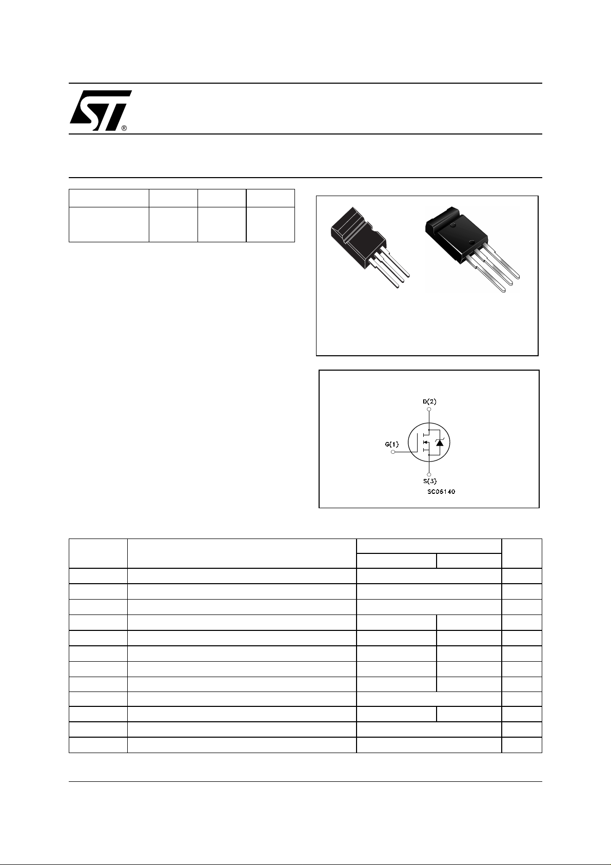
3
2
1
Max220
Max220I
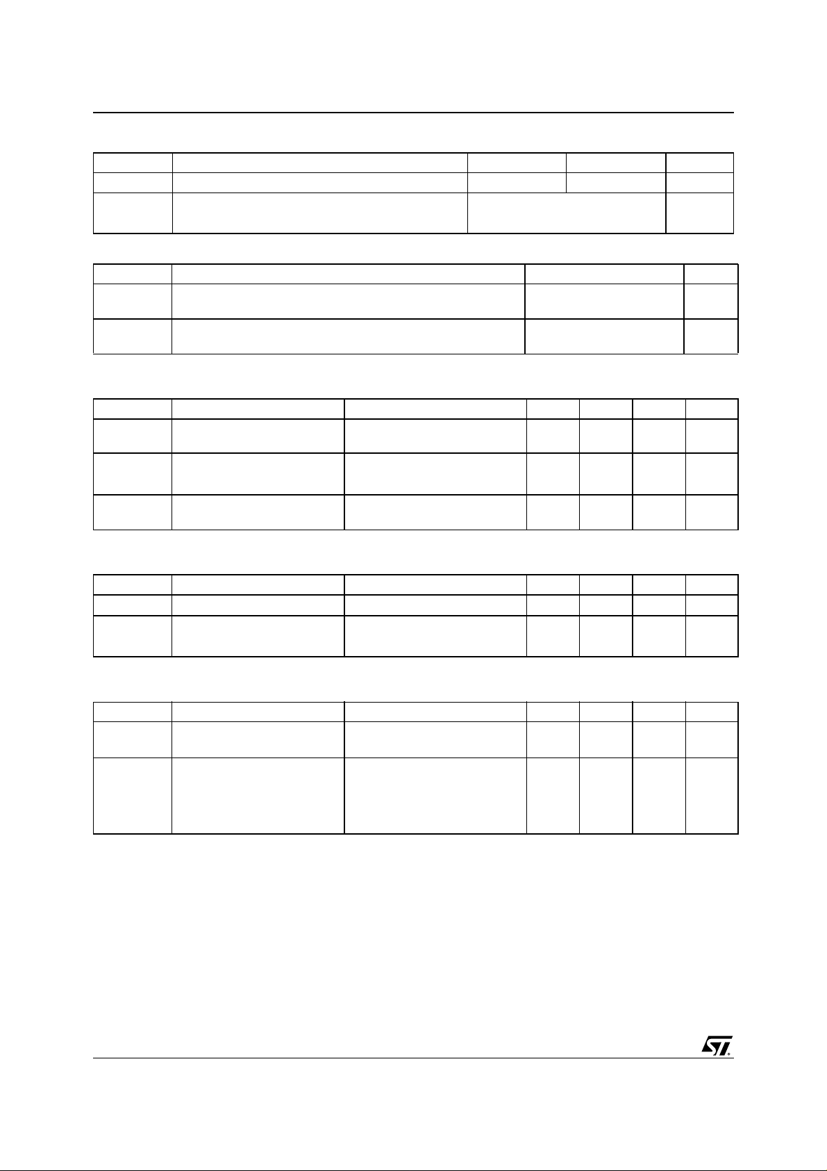
INTERNAL SCHEMATIC DIAGRAM
ABSOLUTE MAXIMUM RATINGS
Symbol Parameter Value Unit
STU7NB90 STU7NB90I
V
DS
V
DGR
V
GS
I
D
I
D
I
DM
P
TOT
dv/dt (1) Peak Diode Recovery voltage slope 4 V/ns
V
ISO
T
stg
T
j
(•)Pu l se width limited by safe operating area
Drain-source Voltage (VGS = 0)
Drain-gate Voltage (RGS = 20 kΩ)
900 V
900 V
Gate- source Voltage ±30 V
Drain Current (continuos) at TC = 25°C
Drain Current (continuos) at TC = 100°C
(●)
Drain Current (pulsed) 29.2 29.2 (*) A
Total Dissipation at TC = 25°C
7.3 7.3 (*) A
4.6 4.6 (*) A
170 60 W
Derating Factor 1.36 0.47 W/°C
Insulation Withstand Voltage (DC) - 2500 V
Storage Temperature –65 to 150 °C
Max. Operating Junction Temperature 150 °C
(1) ISD ≤7.3 A, di/dt ≤200A/µs, VDD ≤ V
(*) Curren t Lim i ted by Pack age
(BR)DSS
, Tj ≤ T
JMAX.
1/9May 2001
Page 2
STU7NB90 - STU7NB90I
THERMA L D ATA
Max220 Max220 I
Rthj-case Thermal Resistance Junction-case Max 0.734 2.1 °C/W
Rthj-amb Thermal Resistance Junction-ambient Max 62.5 °C/W
T
l
AVALANCHE CHARACTERISTICS
Symbol Parameter Max Value Unit
I
AR
E
AS
ELECTRICAL CHARACTERISTICS (TCASE = 25 °C UNLESS OTHERWISE SPECIFIED)
OFF
Symbol Parameter Test Conditions Min. Typ. Max. Unit
V
(BR)DSS
I
DSS
I
GSS
Maximum Lead Temperature For Soldering Purpose 300 °C
Avalanche Current, Repetitive or Not-Repetitive
(pulse width limited by T
max)
j
Single Pulse Avalanche Energy
(starting T
Drain-source
= 25 °C, ID = IAR, VDD = 50 V)
j
ID = 250 µA, VGS = 0 900 V
7.3 A
600 mJ
Breakdown Voltage
Zero Gate Voltage
Drain Current (V
GS
Gate-body Leakage
Current (V
DS
= 0)
= 0)
V
= Max Rating
DS
V
= Max Rating, TC = 125 °C
DS
V
= ±30V ±100 nA
GS
1µA
50 µA
ON (1)
Symbol Parameter Test Conditions Min. Typ. Max. Unit
V
V
GS(th)
R
DS(on)
Gate Threshold Voltage
Static Drain-source On
= VGS, ID = 250 µA
DS
VGS = 10 V, ID = 4 A
234V
1.1 1.45
Resistance
DYNAMIC
Symbol Parameter Test Conditions Min. Typ. Max. Unit
(1) Forward Transconductance VDS > I
g
fs
C
iss
C
oss
C
rss
Input Capacitance
Output Capacitance 225 pF
Reverse Transfer
Capacitance
ID=4 A
V
DS
D(on)
x R
DS(on)max,
= 25V, f = 1 MHz, VGS = 0
8S
2120 pF
23 pF
Ω
2/9
Page 3
STU7NB90 - STU7NB90I
ELECTRICAL CHARACTERISTICS (CONTINUED)
SWITCHING ON
Symbol Parameter Test Conditions Min. Typ. Max. Unit
V
t
d(on)
Q
Q
Q
t
r
g
gs
gd
Turn-on Delay Time
Rise Time 12 ns
Total Gate Charge
Gate-Source Charge 12.5 nC
Gate-Drain Charge 23.5 nC
SWITCHING OFF
Symbol Parameter Test Conditions Min. Typ. Max. Unit
t
r(Voff)
t
t
f
c
Off-voltage Rise Time
Fall Time 15 ns
Cross-over Time 31 ns
SOURCE DRAIN DIODE
Symbol Parameter Test Conditions Min. Typ. Max. Unit
I
SD
I
SDM
VSD (1)
t
rr
Q
rr
I
RRM
Note: 1. Pulsed: Pu l se duration = 300 µs, duty cycle 1.5 %.
2. Pulse width li mited by safe operating ar ea.
Source-drain Current 7.3 A
(2)
Source-drain Current (pulsed) 29.2 A
Forward On Voltage
Reverse Recovery Time
Reverse Recovery Charge 6.3 µC
Reverse Recovery Current 18 A
= 450 V, ID = 3.5 A
DD
RG= 4.7Ω VGS = 10 V
(see test circuit, Figure 3)
V
= 720V, ID = 7.4A,
DD
VGS = 10V
V
= 720V, ID = 7.4 A,
DD
RG=4.7Ω, V
GS
= 10V
(see test circuit, Figure 5)
ISD = 7.3 A, VGS = 0
I
= 7.4 A, di/dt = 100A/µs,
SD
VDD = 100V, Tj = 150°C
(see test circuit, Figure 5)
25 ns
51 72 nC
22 ns
1.6 V
700 ns
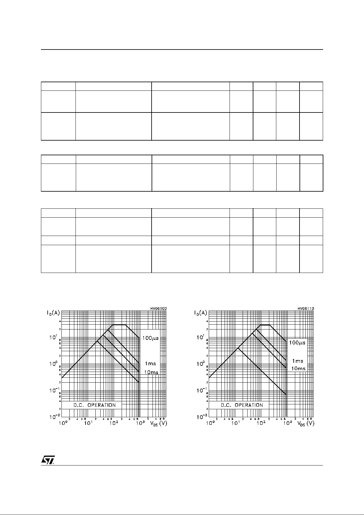
Safe Operating Area for Max220ISafe Operating Area for Max220
3/9
Page 4

STU7NB90 - STU7NB90I
Thermal Impedence for Max220IThermal Impedence for Max220
Output Characteristics Transfer Characteristics
4/9
Static Drain-source On ResistanceTransconductance
Page 5

STU7NB90 - STU7NB90I
Capacitance VariationsGate Charge vs Gate-source Voltage
Normalized Gate Thereshold Voltage vs Temp. Normalized On Resistance vs Temperature
Source-drain Diode Forward Characteristics
5/9
Page 6

STU7NB90 - STU7NB90I
Fig. 2: Unclamped Inductive WaveformFig. 1: Unclamped Inductive Load Test Circuit
Fig. 3: Switching Times Test Circuit For
Resistive Load
Fig. 5: Test Circuit For Inductive Load Switching
And Diode Recovery Times
Fig. 4: Gate Charge test Circuit
6/9
Page 7

Max220 MECHANICAL DATA
STU7NB90 - STU7NB90I
DIM.
MIN. TYP. MAX. MIN. TYP. MAX.
A 4.3 4.6 0.169 0.181
A1 2.2 2.4 0.087 0.094
A2 2.9 3.1 0.114 0.122
b 0.7 0.93 0.027 0.036
b1 1.25 1.4 0.049 0.055
b2 1.2 1.38 0.047 0.054
c 0.45 0.6 0.18 0.023
D 15.9 16.3 0.626 0.641
D1 9 9.35 0.354 0.368
D2 0.8 1.2 0.031 0.047
D3 2.8 3.2 0.110 0.126
e 2.44 2.64 0.096 0.104
E 10.05 10.35 0.396 0.407
L 13.2 13.6 0.520 0.535
L1 3 3.4 0.118 0.133
D3 D1
A
mm inch
D2
A2
C
A1
D
b1
b2
E
L1
L
b
e
P011R
7/9
Page 8

STU7NB90 - STU7NB90I
I-Max220 MECHANICAL DATA
DIM.
MIN. TYP. MAX. MIN. TYP. MAX.
A 4.3 4.6 0.169 0.18 1
A1 2.6 2.75 0.102 0.108
A2 1.95 2.15 0.077 0.084
b 0.7 0.93 0.027 0.036
b1 1.25 1.4 0.049 0.055
b2 1.2 1.38 0.047 0.054
c 0.45 0.6 0.017 0.023
D 15.9 16.3 0.626 0.641
D1 12.5 12.9 0.492 0.508
D2 0.6 1 0.023 0.039
D3 1.75 2.15 0.069 0.084
e 2.44 2.64 0.096 0.104
E 10.05 10.35 0.396 0.407
L 13.2 13.6 0.520 0.535
L1 3 3.4 0.118 0.133
mm inch
8/9
P011S
Page 9

STU7NB90 - STU7NB90I
Information furnished is believed to be accurate and reliable. However, STMicroelectronics assumes no responsibility for the consequences
of use of such informa tion n or for an y infring ement of patent s or other rig hts of third part ies which may resu lt from its use . No l i cen se i s
granted by implication or otherwise under any patent or patent rights of STMicroelectronics. Specification mentioned in this publication are
subject to change without notice. This publication supersedes and replaces all information previously supplied. STMicroelectronics products
are not authorized for use as critical compo nents in life support devices or systems without express written approval of STMicroelectronics.
Australia - Brazil - China - Finland - France - Germany - Hong Kong - India - Italy - Japan - Malaysia - Malta - Morocco -
The ST logo is a trademark of STMicroelectronics
© 2000 STMicroelectronics – Printed in Italy – All Rights Reserved
STMicroelectronics GROUP OF COMPANIES
Singapore - Spain - Sweden - Switzerland - United Kingdom - U.S.A.
http://www.st.com
9/9
 Loading...