

Page 1
®
N - CHANNEL 900V - 1.05 Ω - 7A - Max220
FAST POWER MOS TRANSISTOR
TYPE V
DSS
STU7NA90 900 V < 1.3 Ω 7 A
■ TYPICAL R
■ ± 30V GATE TO SO URCE VO LT AG E
DS(on)
= 1.05 Ω
RANTING
■ 100% AVALANCHE TESTE D
■ REPETITIVE AV A LANCHE DATA AT 100
■ LOW INTRINSIC CAPACITANCE
■ GATE CHARGE MINIMIZED
■ REDUCED VOLTAG E SP REA D
R
DS(on)
STU7NA90
PRELIMINARY DATA
I
D
o
C
3
2
1
APPLICATIONS
■ HIGH CURRENT, HIGH SPEED S WITCHI NG
■ SWITCH MODE PO WE R S UPP LY (S MPS )
■ CONSUMER AND I NDUS TRIA L LI G HTING
■ DC-AC CONVERT E R FOR W E LDI NG
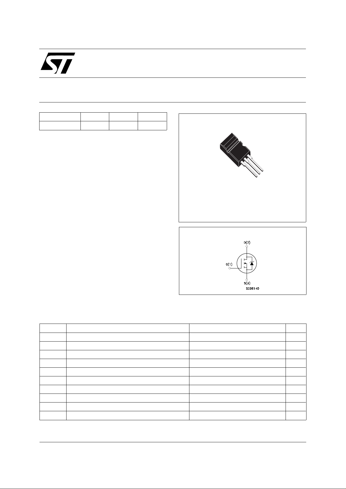
Max220
EQUIPMENT AND UN INTERRUPTABLE
POWER SUPP LY (UPS)
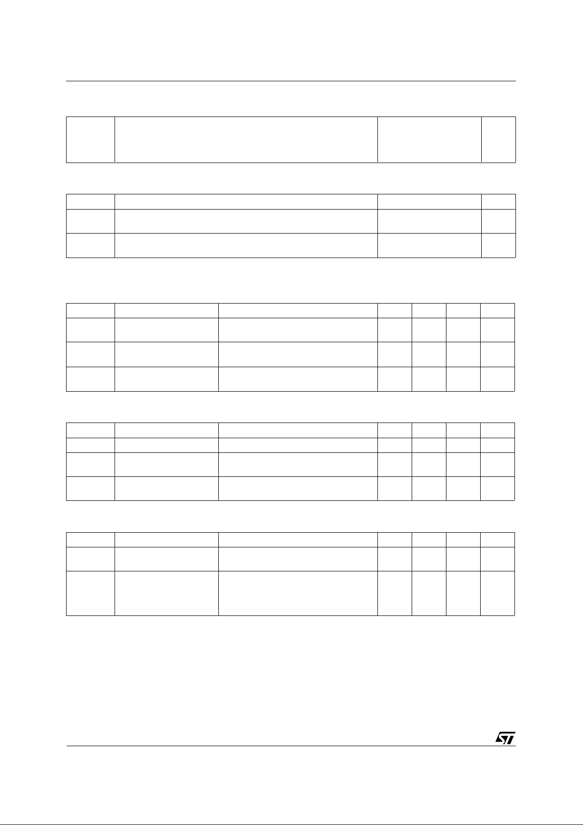
INTERNAL SCHEMAT I C DIAGRAM
ABSOLUTE MA XIMU M RAT INGS
Symbol Parameter Value Unit
V
V
V
IDM(•) Drain Current (pulsed) 28 A
P
T
(•) Pulse width limited by safe operating area
Drain-source Voltage (VGS = 0) 900 V
DS
Drain- gate Voltage (RGS = 20 kΩ)
DGR
Gate-source Voltage ± 30 V
GS
I
Drain Current (continuous) at Tc = 25 oC7A
D
I
Drain Current (continuous) at Tc = 100 oC 4.41 A
D
Total Dissipation at Tc = 25 oC 160 W
tot
Derating Factor 1.28 W/
Storage Temperature -65 to 150
stg
T
Max. Operating Junction Temperature 150
j
900 V
o
C
o
C
o
C
June 1998
1/5
Page 2
STU7NA90
THERMAL DATA
R
thj-case
R
thj-amb
R
thc-si n k
T
Thermal Resistance Junction-case Max
Thermal Resistance Junction-ambient Max
Thermal Resistance Case-sink Typ
Maximum Lead Temperature For Soldering Purpose
l
AVALANCHE CHARACTERISTI CS
Symbol Parameter Max Value Unit
I
AR
E
Avalanche Current, Repetitive or Not-Repetitive
(pulse width limited by T
Single Pulse Avalanche Energy
AS
(starting T
= 25 oC, ID = IAR, V
j
max, δ < 1%)
j
DD
= 25 V)
0.78
30
0.1
300
7A
700 mJ
o
C/W
o
C/W
o
C/W
o
C
ELECTRICAL CHARACTERISTICS (T
= 25 oC unless otherwise specif ied)
case
OFF
Symbol Parameter Test Conditions Min. Typ. Max. Unit
V
(BR)DSS
Drain-source
I
= 250 µA V
D
GS
= 0
900 V
Breakdown Voltage
I
DSS
I
GSS
Zero Gate Voltage
Drain Current (V
GS
Gate-body Leakage
Current (V
DS
= 0)
= 0)
= Max Rating
V
DS
V
= Max Rating Tc = 100oC
DS
V
= ± 30 V
GS
50
500
± 100 nA
ON (∗)
Symbol Parameter Test Conditions Min. Typ. Max. Unit
V
GS(th)
R
DS(on)
Gate Threshold Voltage
Static Drain-source On
= VGS ID = 250 µA
V
DS
VGS = 10 V ID = 3 A 1.05 1.3 Ω
2.25 3 3.75 V
Resistance
I
D(on)
On State Drain Current VDS > I
V
= 10 V
GS
D(on)
x R
DS(on)max
7A
DYNAMIC
Symbol Parameter Test Conditions Min. Typ. Max. Unit
gfs (∗) Forward
Transconductance
C
C
C
Input Capacitance
iss
Output Capacitance
oss
Reverse Transfer
rss
Capacitance
VDS > I
V
DS
x R
D(on)
DS(on)max
= 25 V f = 1 MHz V
ID = 3.5 A 7 9 S
= 0 3100
GS
310
100
4000
400
130
µA
µA
pF
pF
pF
2/5
Page 3

STU7NA90
ELECTRICAL CHARACTERISTICS (continued)
SWITCHING ON
Symbol Parameter Test Conditions Min. Typ. Max. Unit
t
d(on)
t
r
Turn-on Time
Rise Time
V
= 450 V ID = 3.5 A
DD
RG = 4.7 Ω VGS = 10 V
26
18
37
25
ns
ns
Q
Q
Q
Total Gate Charge
g
Gate-Source Charge
gs
Gate-Drain Charge
gd
V
= 720 V ID = 7 A V
DD
= 10 V 125
GS
17
58
175 nC
SWITCHING OFF
Symbol Parameter Test Conditions Min. Typ. Max. Unit
t
r(Voff)
t
t
Off-voltage Rise Time
Fall Time
f
Cross-over Time
c
V
= 720 V ID = 7 A
DD
= 4.7 Ω VGS = 10 V
R
G
34
14
53
48
20
74
SOURCE DRAIN DIODE
Symbol Parameter Test Conditions Min. Typ. Max. Unit
7
28
I
SDM
I
SD
Source-drain Current
(•)
Source-drain Current
(pulsed)
V
(∗) Forward On Voltage ISD = 7 A VGS = 0 1.6 V
SD
t
Q
Reverse Recovery
rr
Time
Reverse Recovery
rr
I
= 7 A di/dt = 100 A/µs
SD
V
= 100 V Tj = 150 oC
DD
810
13
Charge
I
RRM
Reverse Recovery
32
Current
(∗) Pulsed: Pulse duration = 300 µs, duty cycle 1.5 %
(•) Pulse width limited by safe operating area
nC
nC
ns
ns
ns
A
A
ns
µC
A
3/5
Page 4

STU7NA90
Max220 MECHANICAL DATA
DIM.
MIN. TYP. MAX. MIN. TYP. MAX.
A 4.3 4.6 0.169 0.181
A1 2.2 2.4 0.087 0.094
A2 2.9 3.1 0.114 0.122
b 0.7 0.93 0.027 0.036
b1 1.25 1.4 0.049 0.055
b2 1.2 1.38 0.047 0.054
c 0.45 0.6 0.18 0.023
D 15.9 16.3 0.626 0.641
D1 9 9.35 0.354 0.368
D2 0.8 1.2 0.031 0.047
D3 2.8 3.2 0.110 0.126
e 2.44 2.64 0.096 0.104
E 10.05 10.35 0.396 0.407
L 13.2 13.6 0.520 0.535
L1 3 3.4 0.118 0.133
mm inch
D3 D1
D2
C
A
E
A2
A1
D
b1
b2
L1
L
b
e
P011R
4/5
Page 5

STU7NA90
Information furnished is believed to be accurate and reliable. However, STMicroelectronics assumes no responsibility for the consequences
of use of such inform ation nor for any infringe ment o f patents or other rig hts o f third par ties which ma y resul t from i ts use. N o li cen se is
granted by implicatio n or otherwise under any patent or patent rights of STMicroelectronics. Specification mentioned in this publication are
subject to change without notice. This publication supersedes and replaces all information previously supplied. STMicroelectronics products
are not authorized for use as critical compo nents in life support devices or systems without express written approval of STMicroelectronics.
The ST logo is a trademark of STMicroelectronics
© 1998 STMicroelectro nics – Printed in Italy – All Rights Reserved
STMicroelectronics GROUP OF COMPANIES
Australia - Brazil - Canada - China - France - Germany - Italy - Japan - Korea - Malaysia - Malta - Morocco - The Netherlands -
Singapore - Spain - Sweden - Switzerland - Taiwan - Thailand - United Kingdom - U.S.A.
.
5/5
 Loading...