

Page 1
®
N - CHANNEL 1000V - 1.45Ω - 6A - Max220
FAST POWER MOS TRANSISTOR
TYPE V
DSS
STU6NA100 1000 V < 1.7 Ω 6 A
■ TYPICAL R
■ ± 30V GATE TO SOURCE VOLTA GE
DS(on)
= 1.45 Ω
RANTING
■ 100% AVALANCHE TESTED
■ REPETITIVE AVA LANCHE DATA AT 100
■ LOW INTRINSIC CAPACITANCE
■ GATE CHARGE MINIMIZED
■ REDUCED VOLTAGE SPRE AD
R
DS(on)
STU6NA100
PRELIMINARY DATA
I
D
o
C
3
2
1
APPLICATIONS
■ HIGH CURRENT, HIGH SPE ED SWI TCHING
■ SWITCH MODE POWER SUPPLY (SMPS)
■ CONSUMER AND INDU STRI AL LIG HT ING
■ DC-AC CONVERTER FO R WELDING
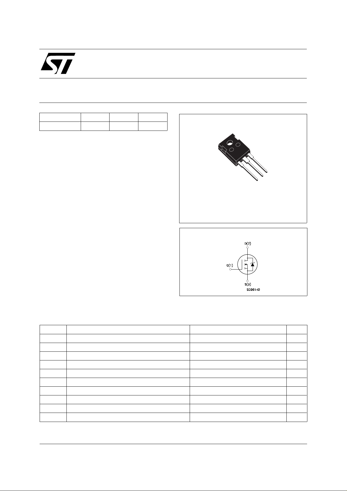
Max220
EQUIPMENT AND UNINTERRUPTABLE
POWER SU PP LY (UP S)
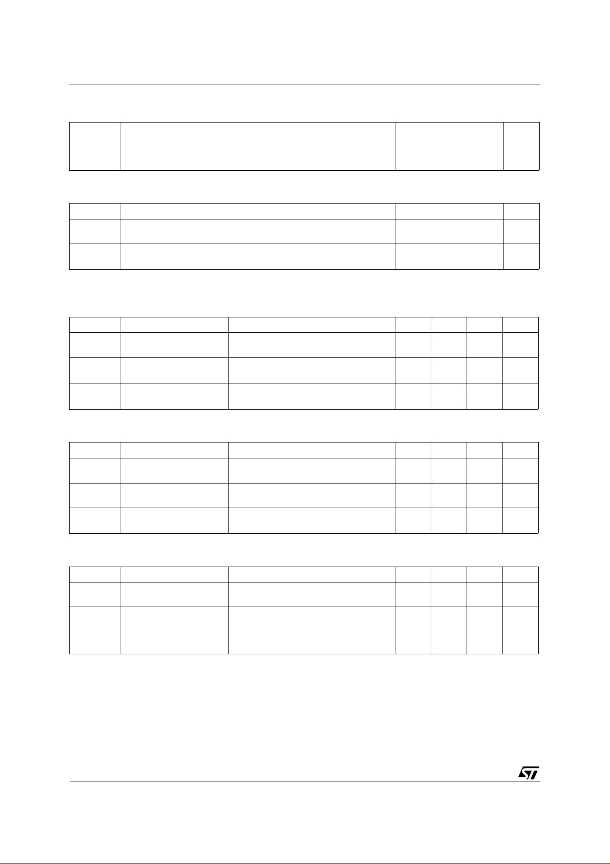
INTER NAL SCH E M ATI C DIAG RA M
ABSOLUTE MAXIMUM RATINGS
Symbol Parameter Value Unit
V
V
V
IDM(•) Drain Current (pulsed) 24 A
P
T
(•) Pulse width limited by safe operating area
Drain-source Voltage (VGS = 0) 1000 V
DS
Drain- gate Voltage (RGS = 20 kΩ)
DGR
Gate-source Voltage ± 30 V
GS
I
Drain Current (continuous) at Tc = 25 oC6A
D
I
Drain Current (continuous) at Tc = 100 oC 3.9 A
D
Total Dissipation at Tc = 25 oC 160 W
tot
Derating Factor 1.28 W/
Storage Temperature -65 to 150
stg
T
Max. Operating Junction Temperature 150
j
1000 V
o
C
o
C
o
C
June 1998
1/5
Page 2
STU6NA100
THERMAL DATA
R
thj-case
R
thj-amb
R
thc-si n k
T
Thermal Resistance Junction-case Max
Thermal Resistance Junction-ambient Max
Thermal Resistance Case-sink Typ
Maximum Lead Temperature For Soldering Purpose
l
AVALANCHE CHARACTERI S TICS
Symbol Parameter Max Value Unit
I
AR
E
Avalanche Current, Repetitive or Not-Repetitive
(pulse width limited by T
Single Pulse Avalanche Energy
AS
(starting T
= 25 oC, ID = IAR, V
j
ma x)
j
DD
= 50 V)
0.8
62
0.1
300
6A
800 mJ
o
C/W
o
C/W
o
C/W
o
C
ELECTRICAL CHARACTERISTICS (T
= 25 oC unless otherwise specified)
case
OFF
Symbol Parameter Test Conditions Min. Typ. Max. Unit
V
(BR)DSS
Drain-source
I
= 250 µA V
D
GS
= 0
1000 V
Breakdown Voltage
I
DSS
I
GSS
Zero Gate Voltage
Drain Current (V
GS
Gate-body Leakage
Current (V
DS
= 0)
= 0)
= Max Rating
V
DS
V
= Max Rating Tc = 100oC
DS
V
= ± 30 V
GS
50
500
± 100 nA
ON (∗)
Symbol Parameter Test Conditions Min. Typ. Max. Unit
V
GS(th)
Gate Threshold
V
= VGS ID = 250 µA
DS
2.25 3 3.75 V
Voltage
R
DS(on)
Static Drain-source On
VGS = 10 V ID = 3 A 1.45 1.7 Ω
Resistance
I
D(on)
On State Drain Current VDS > I
V
= 10 V
GS
D(on)
x R
DS(on)max
6A
DYNAMIC
Symbol Parameter Test Conditions Min. Typ. Max. Unit
gfs (∗) Forward
Transconductance
C
C
C
Input Capacitance
iss
Output Capacitance
oss
Reverse Transfer
rss
Capacitance
VDS > I
V
DS
x R
D(on)
DS(on)max
= 25 V f = 1 MHz V
ID = 3 A 6 7 S
76
4100
351
99
= 0 3170
GS
270
µA
µA
pF
pF
pF
2/5
Page 3

STU6NA100
ELECTRICAL CHARACTERISTICS (continued)
SWITCHING O N
Symbol Parameter Test Conditions Min. Typ. Max. Unit
t
d(on)
t
r
Turn-on Time
Rise Time
V
= 500 V ID =
DD
3.5 A
R
= 4.7 Ω VGS = 10 V
G
28
19
40
27
ns
ns
Q
Q
Q
Total Gate Charge
g
Gate-Source Charge
gs
Gate-Drain Charge
gd
VDD = 800 V ID = 7 A V
= 10 V 125
GS
150 nC
17
58
SWITCHING O F F
Symbol Parameter Test Conditions Min. Typ. Max. Unit
t
r(Voff)
t
t
Off-voltage Rise Time
Fall Time
f
Cross-over Time
c
V
= 800 V ID = 7 A
DD
= 4.7 Ω VGS = 10 V
R
G
35
15
55
50
21
77
SOURCE DRAIN DIO DE
Symbol Parameter Test Conditions Min. Typ. Max. Unit
6
24
I
SDM
I
SD
Source-drain Current
(•)
Source-drain Current
(pulsed)
V
(∗) Forward On Voltage ISD = 6 A VGS = 0 1.6 V
SD
t
Q
Reverse Recovery
rr
Time
Reverse Recovery
rr
I
= 6 A di/dt = 100 A/µs
SD
V
= 100 V Tj = 150 oC
DD
835
14
Charge
I
RRM
Reverse Recovery
33
Current
(∗) Pulsed: Pulse duration = 300 µs, duty cycle 1.5 %
(•) Pulse width limited by safe operating area
nC
nC
ns
ns
ns
A
A
ns
µC
A
3/5
Page 4

STU6NA100
Max220 MECHANICAL DATA
DIM.
MIN. TYP. MAX. MIN. TYP. MAX.
A 4.3 4.6 0.169 0.181
A1 2.2 2.4 0.087 0.094
A2 2.9 3.1 0.114 0.122
b 0.7 0.93 0.027 0.036
b1 1.25 1.4 0.049 0.055
b2 1.2 1.38 0.047 0.054
c 0.45 0.6 0.18 0.023
D 15.9 16.3 0.626 0.641
D1 9 9.35 0.354 0.368
D2 0.8 1.2 0.031 0.047
D3 2.8 3.2 0.110 0.126
e 2.44 2.64 0.096 0.104
E 10.05 10.35 0.396 0.407
L 13.2 13.6 0.520 0.535
L1 3 3.4 0.118 0.133
mm inch
D3 D1
D2
C
A
E
A2
A1
D
b1
b2
L1
L
b
e
P011R
4/5
Page 5

STU6NA100
Information furnished is believed to be accurate and reliable. However, STMicroelectronics assumes no responsibility for the consequences
of use of such information n or for any infrin gement of patents or othe r rights of third parties which may result from its use. No licens e i s
granted by implication or otherwise under any patent or patent rights of STMicroelectronics. Specification mentioned in this publication are
subject to change without notice. This publication supersedes and replaces all information previously supplied. STMicroelectronics products
are not authorized for use as critical components in life support devices or systems without express written approval of STMicroelectronics.
Australia - Brazil - Canada - China - France - Germany - Italy - Japan - Korea - Malaysia - Malta - Mexico - Morocco - The Netherlands -
Singapore - Spain - Sweden - Switzerland - Taiwan - Thailand - United Kingdom - U.S.A.
The ST logo is a trademark of STMicroelectronics
© 1998 STMicroelectronics – Printed in Italy – All Rights Reserved
STMicroelectronics GROUP OF COMPANIES
.
5/5
 Loading...