

Page 1
®
TURBO 2 ULTRAFAST HIGH VOLTAGE RECTIFIER
Table 1: Main Product Characteristics
I
F(AV)
V
I
(max)
R
V
F
(typ)
t
rr
RRM
T
j
(typ)
3 A
600 V
100 µA
175°C
1.0 V
35 ns
STTH3R06
KA
FEATURES AND BENEFITS
■ Ultrafast switching
■ Low forward voltage drop
■ Low thermal resistance
■ Low leakage current (platinium doping)
DESCRIPTION
The STTH3R06, which is using ST Turbo 2 600V
technology, is specially suited for use in switching
power supplies, inverters and as a free wheeling
diode.
Table 2: Order Codes
Part Number Marking
STTH3R06 STTH3R06
STTH3R06RL STTH3R06
STTH3R06U 3R6U
STTH3R06S R6S
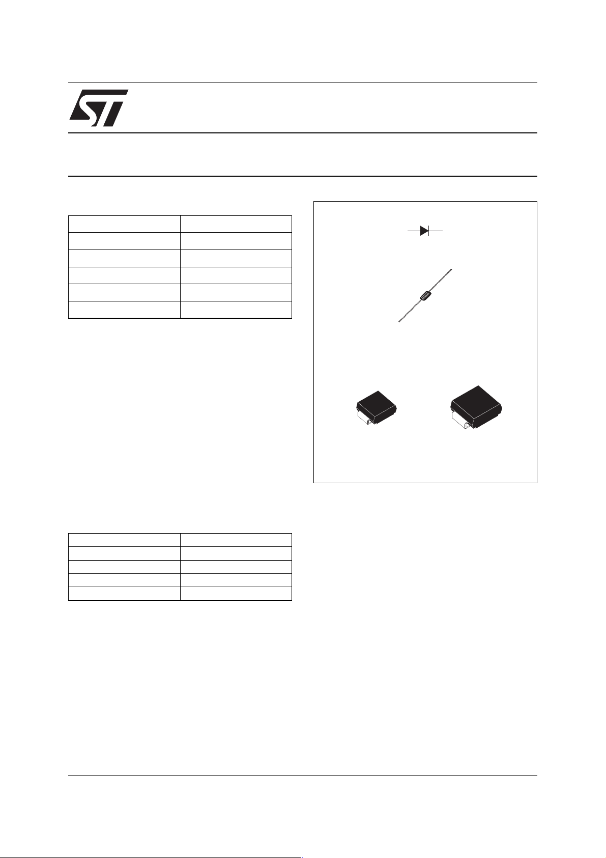
SMB
STTH3R06U
DO-201AD
STTH3R06
SMC
STTH3R06S
September 2005 REV. 3
1/9
Page 2

STTH3R06
Table 3: Absolute Ratings (limiting values)
Symbol Parameter Value Unit
V
RRM
I
F(RMS)
I
F(AV)
I
FSM
T
T
Table 4: Thermal Parameters
Symbol Parameter Maximum Unit
R
th(j-l)
R
th(j-a)
Repetitive peak reverse voltage 600 V
RMS forward current 10 A
Average forward current
δ = 0.5
DO-201AD Tl = 80°C 3 A
SMB Tl = 55°C
SMC Tl = 80°C
Surge non repetitive forward current DO-201AD tp = 10ms
SMB / SMC 45
Storage temperature range -65 to + 175 °C
stg
Maximum operating junction temperature 175 °C
j
sinusoidal
55 A
Junction to lead DO-201AD L = 10 mm 20 °C/W
SMB 25
SMC 20
Junction to ambient (see fig. 13) DO-201AD L = 10 mm 75 °C/W
Table 5: Static Electrical Characteristics
Symbol Parameter Test conditions Min. Typ Max. Unit
I
V
To evaluate the conduction losses use the following equation: P = 1.03 x I
Reverse leakage current Tj = 25°C VR = V
R
= 150°C 15 100
T
j
Forward voltage drop Tj = 25°C IF = 3A 1.7 V
F
= 150°C 1.0 1.25
T
j
F(AV)
RRM
+ 0.09 I
F2(RMS)
3µA
Table 6: Dynamic Characteristics
Symbol Parameter Test conditions Min. Typ Max. Unit
t
Reverse recovery
rr
time
t
Forward recovery
fr
time
V
Forward recovery
FP
Tj = 25°C IF = 0.5A IRR = 0.25A IR = 1A 30 ns
I
= 1A dIF/dt = -50 A/µs VR =30V 35
F
Tj = 25°C IF = 3A dIF/dt = 100 A/µs
= 1.1 x V
V
FR
Fmax
100 ns
IF = 3A dIF/dt = 100 A/µs 10 V
voltage
2/9
Page 3
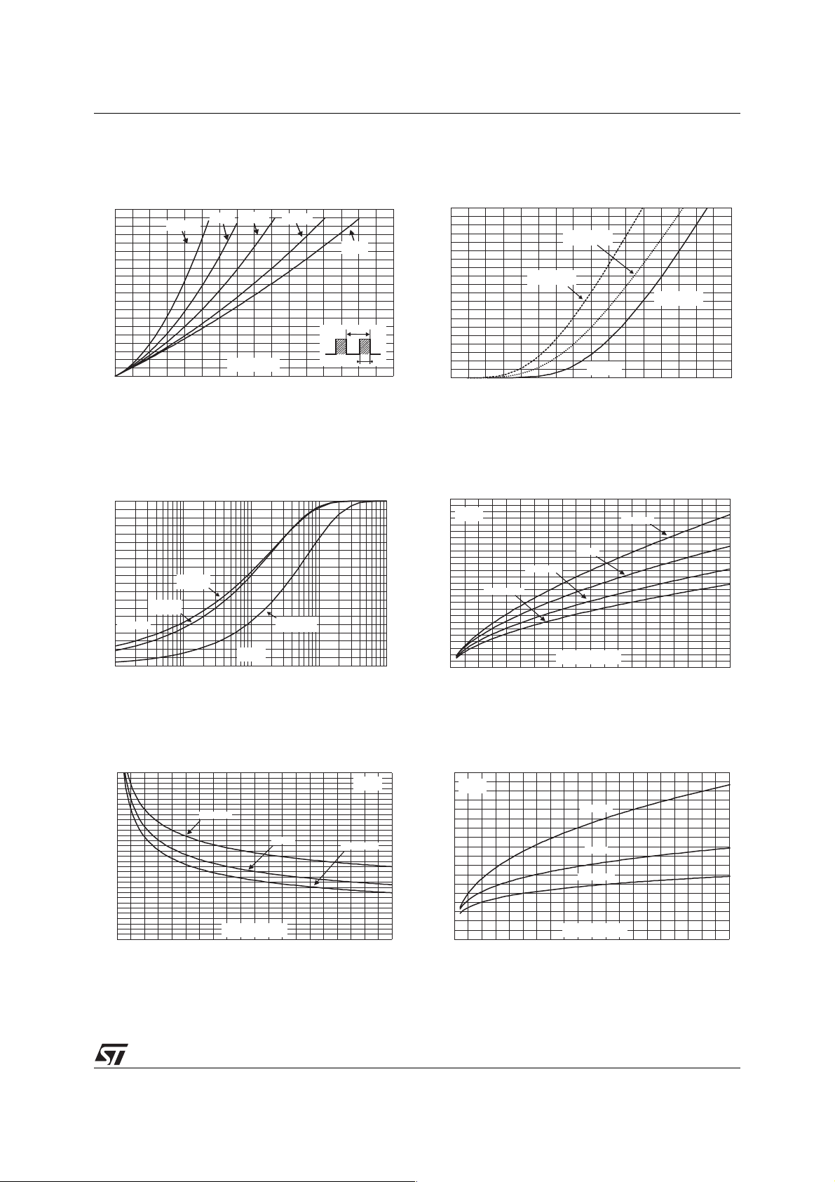
STTH3R06
Figure 1: Conduction losses versus average
current
P(W)
5.0
4.5
4.0
3.5
3.0
2.5
2.0
1.5
1.0
0.5
0.0
0.0 0.5 1.0 1.5 2.0 2.5 3.0 3.5 4.0
δ = 0.05
δ = 0.1
δ = 0.2
I (A)
F(AV)
δ = 0.5
δ
=tp/T
δ = 1
T
tp
Figure 3: Relative variation of thermal impedance
junction ambient versus pulse duration (epoxy
printed circuit FR4, L
Z/R
th(j-a) th(j-a)
1.0
0.9
0.8
0.7
0.6
0.5
0.4
0.3
Single pulse
0.2
0.1
0.0
1.E-01 1.E+00 1.E+01 1.E+02 1.E+03
SMB
S = 1cm
Cu
SMC
S = 1cm
Cu
2
2
= 10mm, SCU=1cm2)
leads
DO-201AD
L = 10mm
leads
t (s)
p
Figure 2: Forward voltage drop versus forward
current
I (A)
FM
50
45
40
35
30
25
20
15
10
5
0
0.0 0.5 1.0 1.5 2.0 2.5 3.0 3.5 4.0
(typical values)
T =150°C
j
T =150°C
j
(maximum values)
V (V)
FM
T =25°C
j
(maximum values)
Figure 4: Peak reverse recovery current
versus dI
I (A)
RM
13
V =400V
R
12
T =125°C
j
11
10
9
8
7
6
5
4
3
2
1
0
0 50 100 150 200 250 300 350 400 450 500
/dt (typical values)
F
I=I
FF(AV)
I =0.5 x I
FF(AV)
I =0.25 x I
F F(AV)
dI /dt(A/µs)
F
I =2 x I
FF(AV)
Figure 5: Reverse recovery time versus dI
(typical values)
t (ns)
rr
160
150
140
130
120
110
100
90
80
70
60
50
40
30
20
10
0
0 50 100 150 200 250 300 350 400 450 500
I =2 x I
F F(AV)
dI /dt(A/µs)
F
I=I
F F(AV)
V =400V
R
T =125°C
j
I =0.5 x I
F F(AV)
/dt
F
Figure 6: Reverse recovery charges versus
dI
/dt (typical values)
F
Q (nC)
rr
450
V =400V
R
T =125°C
j
400
I =2 x I
350
FF(AV)
300
250
200
150
I=I
FF(AV)
I =0.5 x I
FF(AV)
100
50
0
dI /dt(A/µs)
F
0 50 100 150 200 250 300 350 400 450 500
3/9
Page 4
STTH3R06
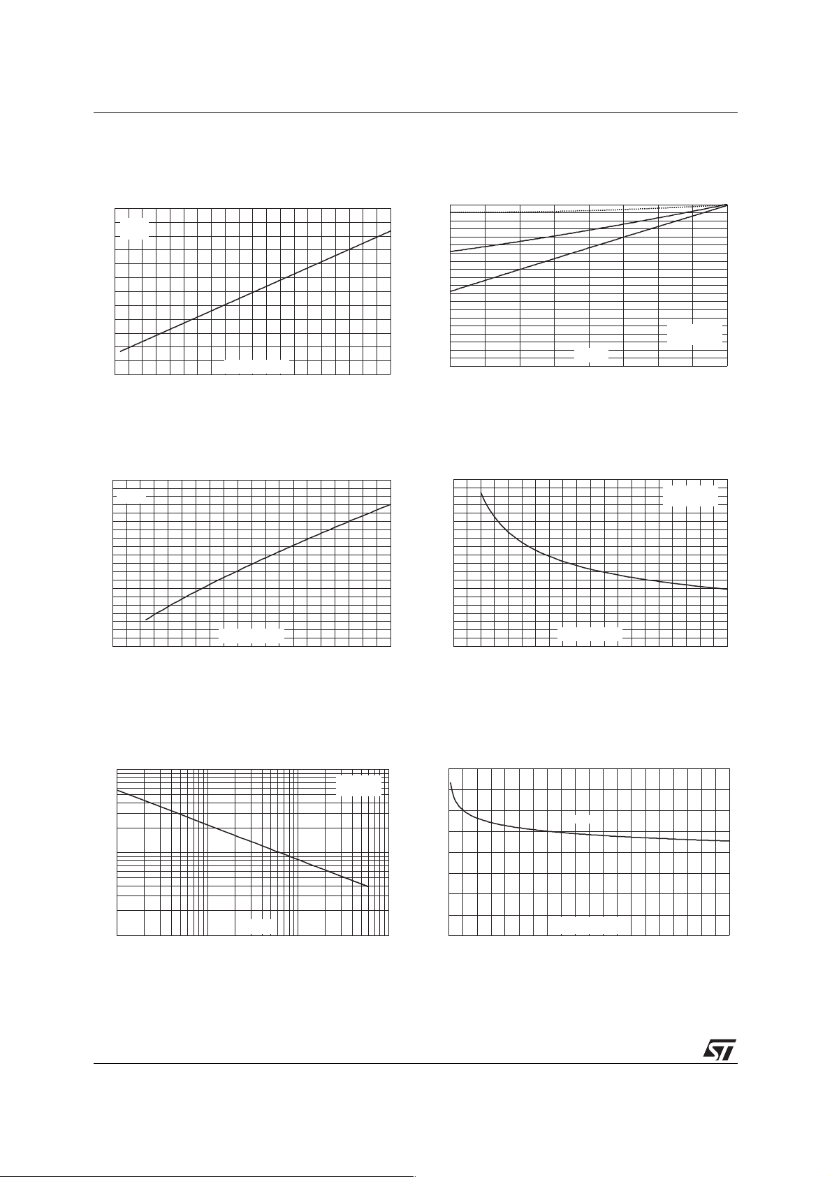
Figure 7: Softness factor versus dIF/dt (typical
values)
S factor
3.0
I=I
F F(AV)
V =400V
R
T =125°C
j
2.5
2.0
1.5
1.0
0.5
dI /dt(A/µs)
0.0
0 50 100 150 200 250 300 350 400 450 500
F
Figure 9: Transient peak forward voltage
versus dI
V (V)
FP
20
I=I
F F(AV)
18
T =125°C
16
14
12
10
8
6
4
2
0
0 20 40 60 80 100 120 140 160 180 200
/dt (typical values)
F
j
dI /dt(A/µs)
F
Figure 8: Relative variations of dynamic
parameters versus junction temperature
1.0
0.9
0.8
0.7
0.6
0.5
0.4
0.3
0.2
0.1
0.0
Q
RR
25 50 75 100 125
Figure 10: Forward recovery time versus dI
S factor
I
RM
I=I
F F(AV)
V =400V
R
Reference:T =125°C
j
T (°C)
j
/dt
F
(typical values)
t (ns)
fr
200
180
160
140
120
100
80
60
40
20
0
0 20 40 60 80 100 120 140 160 180 200
dI /dt(A/µs)
F
I=I
F F(AV)
V =1.1 x V max.
FR F
T =125°C
j
Figure 11: Junction capacitance versus
reverse voltage applied (typical values)
C(pF)
100
10
V (V)
1
1 10 100 1000
R
4/9
F=1MHz
V =30mV
OSC RMS
T =25°C
j
Figure 12: Thermal resistance junction to
ambient versus copper surface under lead
(epoxy FR4, e
R (°C/W)
th(j-a)
80
70
60
50
40
30
20
10
0
012345678910
=35µm) (DO-201AD)
CU
DO-201AD
S (cm²)
CU
Page 5
STTH3R06
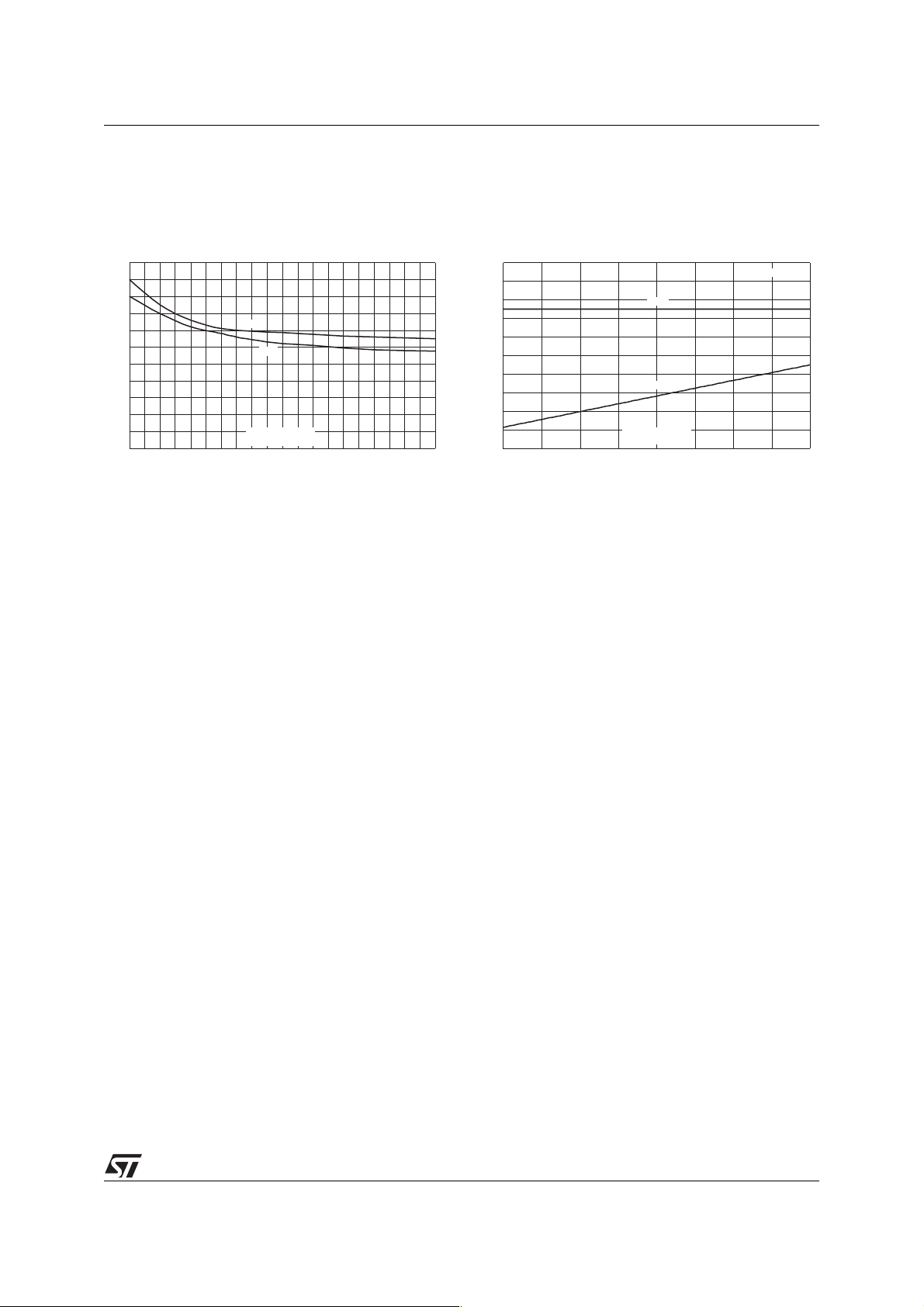
Figure 13: Thermal resistance junction to
ambient versus copper surface under lead
(epoxy FR4, e
R (°C/W)
th(j-a)
110
100
90
80
70
60
50
40
30
20
10
0
0.0 0.5 1.0 1.5 2.0 2.5 3.0 3.5 4.0 4.5 5.0
=35µm) (SMB / SMC)
CU
SMB
SMC
S (cm²)
CU
Figure 14: Thermal resistance versus lead
length
R (°C/W)
th
100
90
80
70
60
50
40
30
20
10
0
5 10152025
R
th(j-a)
R
th(j-l)
L (mm)
lead
DO-201AD
5/9
Page 6
STTH3R06
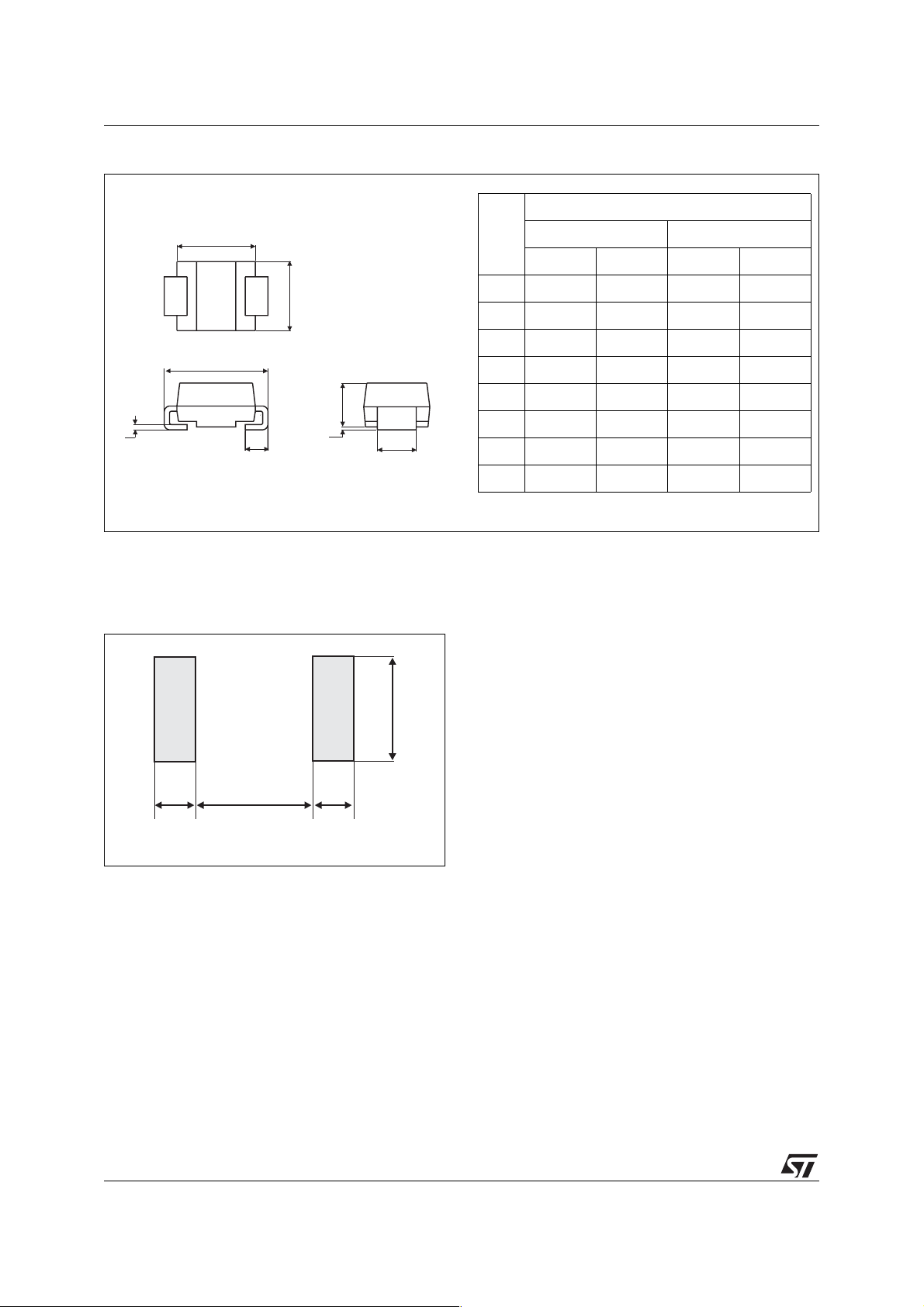
Figure 15: SMB Package Mechanical Data
DIMENSIONS
E1
D
E
A1
C
L
A2
Figure 16: SMB Foot Print Dimensions
(in millimeters)
REF.
Millimeters Inches
Min. Max. Min. Max.
A1 1.90 2.45 0.075 0.096
A2 0.05 0.20 0.002 0.008
b 1.95 2.20 0.077 0.087
c 0.15 0.41 0.006 0.016
E 5.10 5.60 0.201 0.220
E1 4.05 4.60 0.159 0.181
b
D 3.30 3.95 0.130 0.156
L 0.75 1.60 0.030 0.063
1.52 2.75
2.3
1.52
6/9
Page 7
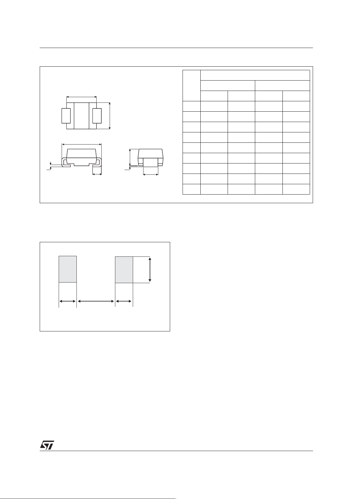
Figure 17: SMC Package Mechanical Data
STTH3R06
DIMENSIONS
E1
D
E
A1
C
L
A2
Figure 18: SMC Foot Print Dimensions
(in millimeters)
REF.
Millimeters Inches
Min. Max. Min. Max.
A1 1.90 2.45 0.075 0.096
A2 0.05 0.20 0.002 0.008
b 2.90 3.2 0.114 0.126
c 0.15 0.41 0.006 0.016
E 7.75 8.15 0.305 0.321
E1 6.60 7.15 0.260 0.281
E2 4.40 4.70 0.173 0.185
b
D 5.55 6.25 0.218 0.246
L 0.75 1.60 0.030 0.063
2.0 4.2 2.0
3.3
7/9
Page 8
STTH3R06
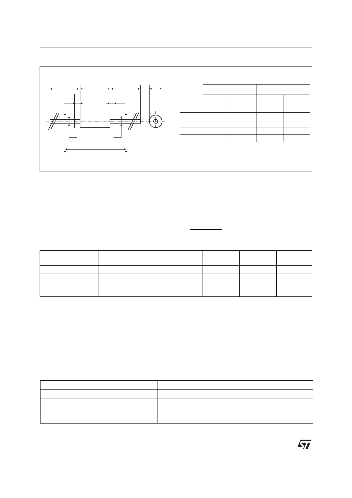
Figure 19: DO-201AD Package Mechanical Data
BA
B
ØC
REF.
DIMENSIONS
Millimeters Inches
note 1
E
note 1
E
Min. Max. Min. Max.
A9.500.374
B 25.40 1.000
C5.300.209
D1.300.051
ØD ØD
note 2
E 1.25 0.049
1 - The lead diameter ø D is not controlled over zone E
NOTES
2 - The minimum axial length within which the device
may be placed with its leads bent at right angles is
0.59"(15 mm)
In order to meet environmental requirements, ST offers these devices in ECOPACK® packages. These
packages have a Lead-free second level interconnect . The category of second level interconnect is
marked on the package and on the inner box label, in compliance with JEDEC Standard JESD97. The
maximum ratings related to soldering conditions are also marked on the inner box label. ECOPACK is an
ST trademark. ECOPACK specifications are available at: www.st.com
.
Table 7: Ordering Information
Ordering type Marking Package Weight Base qty
Delivery
mode
STTH3R06 STTH3R06 DO-201AD 1.12 g 600 Ammopack
STTH3R06-RL STTH3R06 DO-201AD 1.12 g 1900 Tape & reel
STTH3R06U 3R6U SMB 0.11 g 2500 Tape & reel
STTH3R06S R6S SMC 0.243 g 2500 Tape & reel
■ Epoxy meets UL94, V0
■ Band indicated cathode (DO-201AD)
■ Bending method: see application note AN1471 (DO-201AD)
Table 8: Revision History
Date Revision Description of Changes
March-2003 1 First issue
07-Sep-2004 2 SMB and SMC packages added
14-Oct-2005 3 Changed marking of STTH3R06U from R06U to 3R6U on
page 1. Added ECOPACK statement.
8/9
Page 9

STTH3R06
Information furnished is believed to be accurate and reliable. However, STMicroelectronics assumes no responsibility for the consequences
of use of such information nor for any infringement of patents or other rights of third parties which may result from its use. No license is granted
by implication or otherwise under any patent or patent rights of STMicroelectronics. Specifications mentioned in this publication are subject
to change without notice. This publication supersedes and replaces all information previously supplied. STMicroelectronics products are not
authorized for use as critical components in life support devices or systems without express written approval of STMicroelectronics.
The ST logo is a registered trademark of STMicroelectronics.
All other names are the property of their respective owners
© 2005 STMicroelectronics - All rights reserved
Australia - Belgium - Brazil - Canada - China - Czech Republic - Finland - France - Germany - Hong Kong - India - Israel - Italy - Japan -
Malaysia - Malta - Morocco - Singapore - Spain - Sweden - Switzerland - United Kingdom - United States of America
STMicroelectronics group of companies
www.st.com
9/9
 Loading...