

Page 1
®
HIGH EFFICIENCY ULTRAFAST DIODE
MAIN PRODUCT CHARACTERISTICS
STTH302S
I
F(AV)
V
RRM
3A
200 V
Tj (max) 175 °C
(max) 0.75 V
V
F
trr (max) 35 ns
FEATURES AND BENEFITS
Very low conduction losses
■
Negligible switching losses
■
Low forward and reverse recovery times
■
High junction temperature
■
DESCRIPTION
The STTH302S, which is using ST’s new 200V
planar technology, is specially suited for switching
mode base drive & transistor circuits.
The device is also intended for use as a free
wheeling diode in power supplies and other power
switching applications.
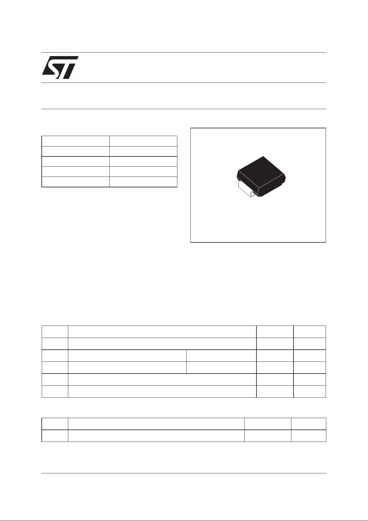
SMC
ABSOLUTE RATINGS (limiting values)
Symbol Parameter Value Unit
V
RRM
I
F(AV)
I
FSM
T
stg
Repetitive peak reverse voltage 200 V
Average forward current Tl = 107°C δ =0.5 3 A
Surge non repetitive forward current tp = 10 ms Sinusoidal 100 A
Storage temperature range - 65 + 175 °C
Tj Maximum operating junction temperature 175 °C
THERMAL PARAMETERS
Symbol Parameter Maximum Unit
R
th (j-l)
April 2002 - Ed: 1A
Junction to lead 20 °C/W
1/5
Page 2
STTH302S
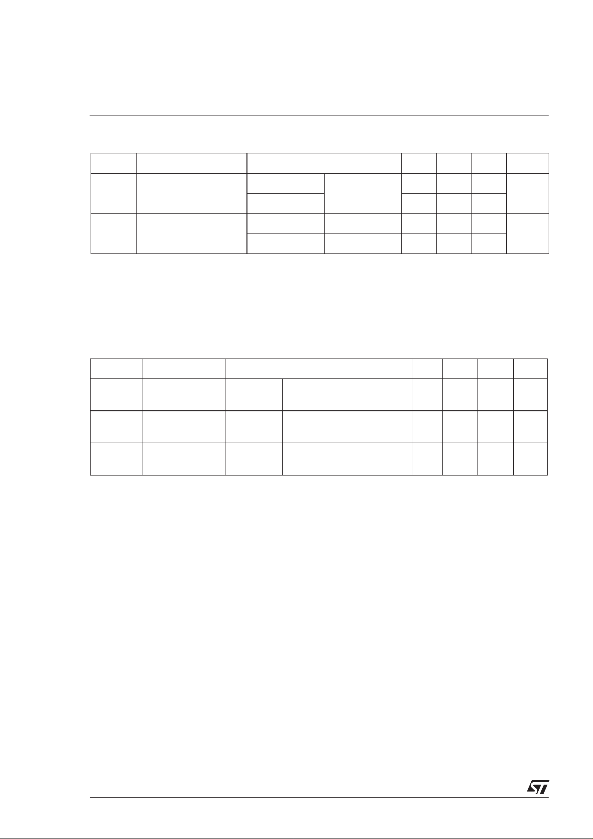
STATIC ELECTRICAL CHARACTERISTICS
Symbol Parameter Tests conditions Min. Typ. Max. Unit
I
* Reverse leakage
R
current
V
** Forward voltage drop Tj= 25°C I
F
Tj = 25°C V
R=VRRM
3 µA
Tj = 125°C 4 75
= 3 A 0.95 V
F
Tj = 125°C I
Pulse test: * tp = 5ms, δ <2%
** tp = 380µs, δ <2%
= 3 A 0.66 0.75
F
To evaluate the maximum conduction losses use the following equation :
P=0.60xI
F(AV)
+ 0.05 I
F2(RMS)
DYNAMIC ELECTRICAL CHARACTERISTICS
Symbol Parameter Tests conditions Min. Typ. Max. Unit
trr Reverse recovery
time
tfr Forward recovery
time
V
FP
Forward recovery
Tj = 25°C I
Tj = 25°C I
Tj = 25°C I
=1 A Irr = -50 A/µs
F
VR= 30V
=3A dIF/dt=50A/µs
F
70 ns
VFR=1.1xVFmax
=3A dIF/dt=50A/µs 1.6 V
F
35 ns
voltage
2/5
Page 3
STTH302S
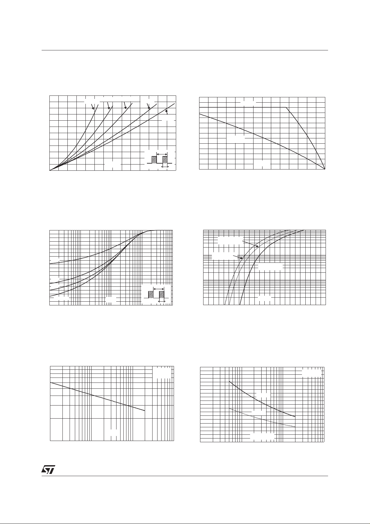
Fig. 1: Average forward power dissipation versus
average forward current.
P (W)F(AV)
3.0
δ = 0.05
2.5
2.0
1.5
1.0
0.5
0.0
0.0 0.5 1.0 1.5 2.0 2.5 3.0 3.5
δ = 0.1
I (A)F(AV)
δ = 0.2
δ = 0.5
δ
=tp/T
δ = 1
T
tp
Fig. 3: Relative variation of thermal impedance
junction ambient versus pulse duration (Printed
circuit board epoxy FR4).
Zth(j-a)/Rth(j-a)
1.0
0.9
0.8
0.7
δ = 0.5
0.6
0.5
0.4
δ = 0.2
0.3
δ = 0.1
0.2
0.1
Single pulse
0.0
1.E-01 1.E+00 1.E+01 1.E+02 1.E+03
tp(s)
δ
=tp/T
T
tp
Fig. 2: Average forward current versus ambient
temperature (δ = 0.5)
I (A)F(AV)
3.5
3.0
2.5
2.0
1.5
1.0
0.5
0.0
0 25 50 75 100 125 150 175
R
th(j-a)=Rth(j-l)
R
=75°C/W
th(j-a)
S=1cm²
T (°C)amb
Fig. 4: Forward voltage drop versus forward
current.
I (A)FM
100.0
Tj=125°C
Tj=125°C
(Maximum values)
(Maximum values)
Tj=125°C
10.0
1.0
0.1
0.0 0.2 0.4 0.6 0.8 1.0 1.2 1.4 1.6 1.8 2.0 2.2 2.4
Tj=125°C
(Typical values)
(Typical values)
Tj=25°C
(Maximum values)
V (V)FM
Fig. 5: Junction capacitance versus reverse
voltage applied (typical values).
C(pF)
100
V (V)R
10
1 10 100 1000
F=1MHz
V
osc
T
=30mV
=25°C
j
Fig. 6: Reverse recovery time versus dIF/dt (90%
confidence).
t (ns)RR
100
90
80
70
60
50
40
30
20
10
0
1 10 100 1000
Tj=125°C
Tj=25°C
dI /dt(A/µs)F
IF=3A
=100V
V
R
3/5
Page 4
STTH302S
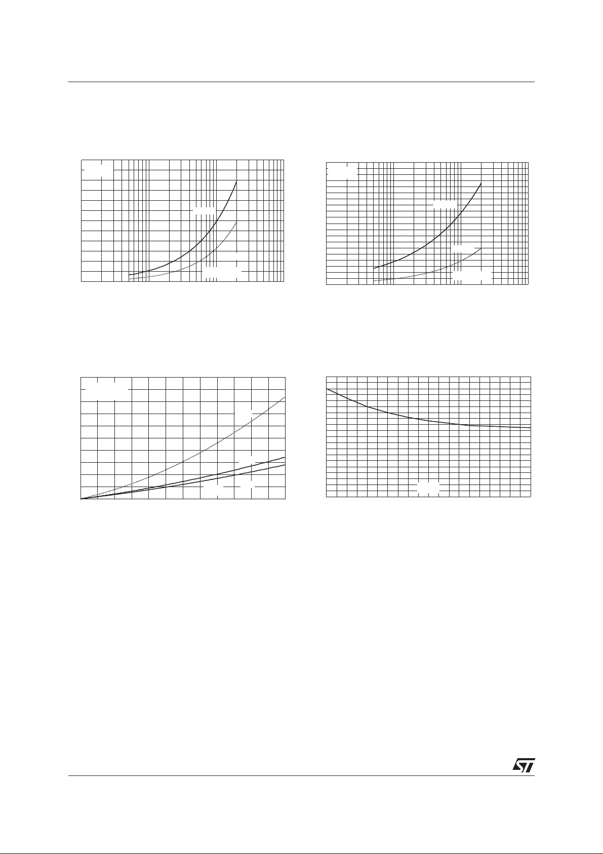
Fig. 7: Peak reverse recovery current versus
/dt (90% confidence).
dI
F
I (A)RM
6.0
IF=3A
=100V
V
R
5.0
4.0
3.0
2.0
1.0
Tj=125°C
Tj=25°C
dI /dt(A/µs)F
0.0
1 10 100 1000
Fig. 9: Relative variations of dynamic parameters
versus junction temperature.
I ;t ; Q [Tj] / I ; t ; Q [Tj = 25°C]RM RR RR RM RR RR
3.5
3.0
2.5
2.0
1.5
1.0
IF=3A
/dt=200A/µs
dI
F
=100V
V
R
Q
RR
t
RR
I
Tj(°C)
25 50 75 100 125 150 175
RM
Fig. 8: Reverse recovery charges versus dIF/dt
(90% confidence).
Q (nC)RR
100
IF=3A
90
=100V
V
R
80
70
60
50
40
30
20
10
0
1 10 100 1000
Tj=125°C
Tj=25°C
dI /dt(A/µs)F
Fig. 10: Thermal resistance junction to ambient
versus copper surface under each lead (epoxy
FR4, e = 35µm).
Rth(j-a)(°C/W)
100
90
80
70
60
50
40
30
20
10
0
0.0 0.5 1.0 1.5 2.0 2.5 3.0 3.5 4.0 4.5 5.0
S(cm²)
4/5
Page 5
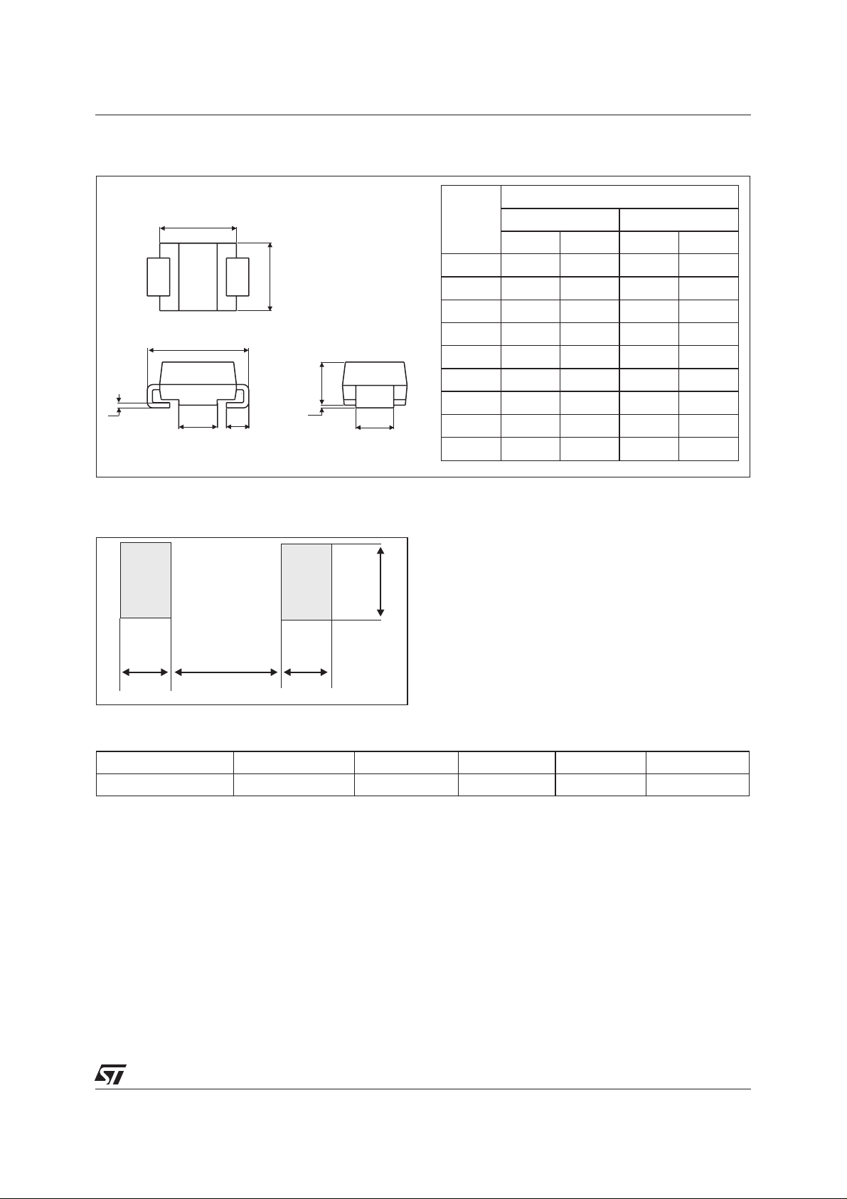
PACKAGE MECHANICAL DATA
SMC
E1
D
E
C
L
E2
STTH302S
DIMENSIONS
REF.
A1 1.90 2.45 0.075 0.096
A2 0.05 0.20 0.002 0.008
b 2.90 3.2 0.114 0.126
c 0.15 0.41 0.006 0.016
E 7.75 8.15 0.305 0.321
A1
A2
b
E1 6.60 7.15 0.260 0.281
E2 4.40 4.70 0.173 0.185
D 5.55 6.25 0.218 0.246
L 0.75 1.60 0.030 0.063
Millimeters Inches
Min. Max. Min. Max.
FOOTPRINT
3.3
2.0 4.2 2.0
Ordering code Marking Package Weight Base qty Delivery mode
STTH302S U32 SMC 0.245 g 2500 Tape & reel
■
Epoxy meets UL 94,V0
Informationfurnished is believedto be accurateand reliable. However,STMicroelectronics assumes noresponsibility for theconsequences of
useof suchinformation nor forany infringement ofpatents or otherrights of thirdparties which mayresult fromits use. Nolicense is grantedby
implication or otherwise under any patent or patent rights of STMicroelectronics. Specifications mentioned in this publication are subject to
change withoutnotice. This publication supersedes and replaces all information previously supplied.
STMicroelectronics products are not authorized for use as critical components in life support devices or systems without express written approval ofSTMicroelectronics.
The ST logo is a registered trademark of STMicroelectronics
© 2002 STMicroelectronics - Printed in Italy - All rights reserved.
STMicroelectronics GROUP OF COMPANIES
Australia - Brazil - Canada - China - Finland - France - Germany
Hong Kong - India - Israel - Italy - Japan - Malaysia - Malta - Morocco - Singapore
Spain - Sweden - Switzerland - United Kingdom - United States.
http://www.st.com
5/5
 Loading...