

Page 1
STT2604
Elektronische Bauelemente
N-Channel Enhancement Mode Power Mos.FET
RoHS Compliant Product
Description
The STT2604 utiltzed advance processing techniques to achieve the lowest
possible on-resistance, extermely efficient and cost-effectiveness device.
The STT2604 is universally used for all commercial-industrial applications.
Features
* Lower Gate Charge
* Fast Switching Characteristic
* Small Footprint & Low Profile Package
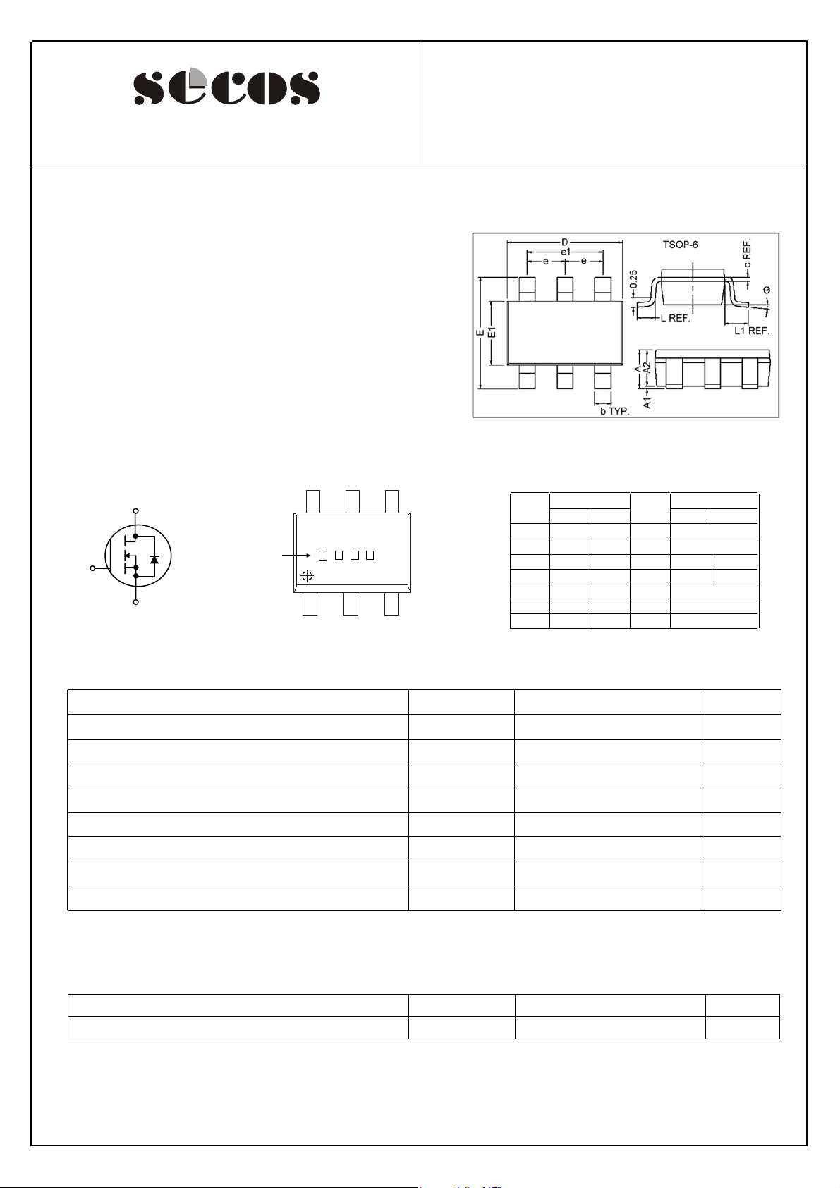
D D S
D
6
2604
G
S
Date Code
1
D D G
4
5
3
2
5.5A, 30V,RDS(ON) 45m
Ω
REF.
Millimeter
Min. Max.
A 1.10 MAX. L 0.45 REF.
A1 0 0.10 L1 0.60 REF.
A2 0.70 1.00 0° 10°
c 0.12 REF. b 0.30 0.50
D 2.70 3.10 e 0.95 REF.
E 2.60 3.00 e1 1.90 REF.
E1 1.40 1.80
REF.
Millimeter
Min. Max.
Absolute Maximum Ratings
Parameter Symbol Ratings Unit
Drain-Source Voltage
Gate-Source Voltage
1,2
3
GS@4.5V
3
GS@4.5V
Continuous Drain Current,V
Continuous Drain Current,V
Pulsed Drain Current
Total Power Dissipation
Linear Derating Factor
Operating Junction and Storage Temperature Range
Thermal Data
Parameter
Thermal Resistance Junction-case
3
Max.
VDS
VGS
D@TC=25
I
I
D@TC=70
I
DM
PD@TC=25
Tj, Tstg
Symbol
Rthj-c
3
0
20
±
o
C
o
C
o
C
5.5
4.4
20
2
0.016
-55~+150
V
V
W / C
A
A
A
W
o
o
C
Ratings Unit
62.5
o
/W C
http://www.SeCoSGmbH.com/ Any changing of specification will not be informed individual
01-Jun-2002 Rev. A
Page 1 of 4
Page 2
STT2604
5.5A, 30V,RDS(ON) 45m
Elektronische Bauelemente
N-Channel Enhancement Mode Power Mos.FET
o
o
C
)
C
o
BV
DSS
BVDS/ Tj
VGS(th)
IGSS
IDSS
RD S( ON )
Qg
Qgs
Qgd
Td
(ON)
Tr
(Off)
Td
T
f
Ciss
Coss
Crss
Min. Unit
30
_
1.0
_
_
_
_
_
_
_
_
_
_
_
_
_
_
_
_
_
Typ.
_
0.02
_
_
_
_
_
_
6
2
3
6
8
15
4
440
105
35
3.0
±
100
705
_
_
1
25
45
65
10
_
_
_
_
_
_
_
_
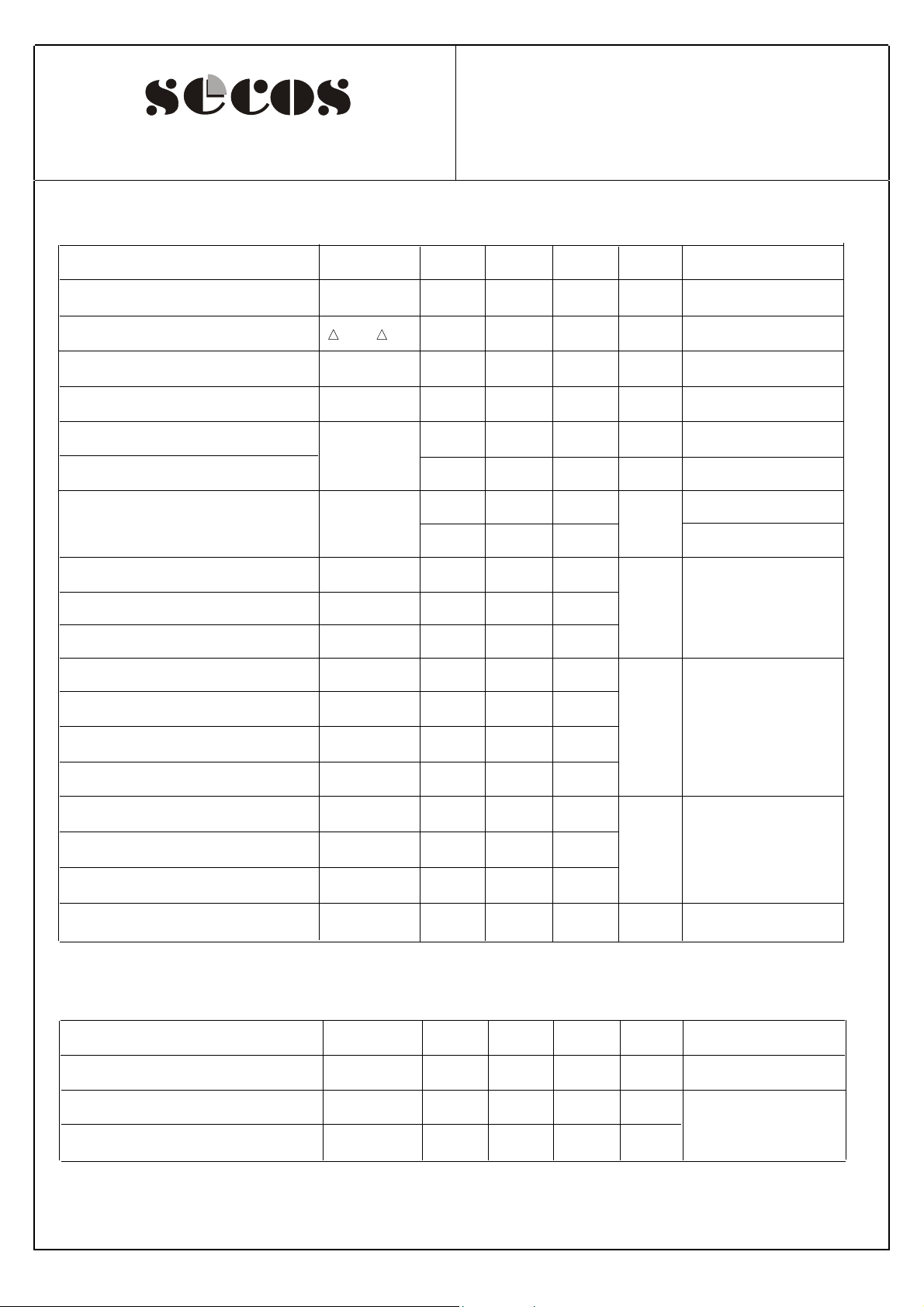
Electrical Characteristics( Tj=25 C Unless otherwise specified)
Parameter Symbol Max.
Drain-Source Breakdown Voltage
Breakdown Voltage Temp. Coefficient
Gate Threshold Voltage
Gate-Source Leakage Current
Drain-Source Leakage Current (Tj=25 )
Drain-Source Leakage Current(Tj=55
Static Drain-Source On-Resistance
Total Gate Charge
2
Gate-Source Charge
Gate-Drain ("Miller") Charge
Turn-on Delay Time
2
Rise Time
Turn-off Delay Time
Fall Time
Input Capacitance
Output Capacitance
Reverse Transfer Capacitance
2
V
o
V/
C
V
nA
uA
uA
Ω
m
nC
nS
pF
Ω
Test Condition
VGS=0V, ID=250uA
Reference to 25 C , I
DS=VGS, ID=250uA
V
±
VGS= 20V
VDS=30V,VGS=0
DS=24V,VGS=0
V
VGS=10V, ID
GS=4.5V, I
V
ID=4.8A
VDS=24V
VGS= 4.5V
VDD=15V
ID=1A
VGS=10V
RG=3.3
Ω
RD=15
GS=0V
V
VDS=25V
f=1.0MHz
o
=4.8A
D=2.4A
Ω
D=1m
A
Forward Transconductance
Gfs
7
__
S
VDS =10V, ID=4.8A
Source-Drain Diode
Parameter Symbol Max.
Forward On Voltage
Reverse Recovery Time
2
2
Reverse Recovery Change
Notes: 1.Pulse width limited by safe operating area.
2.Pulse width 300us, dutycycle 2%.
≦
3.Surface mounted on 1 in2 copper pad of FR4 board; 156OC/W when mounted on Min. copper pad.
http://www.SeCoSGmbH.com/ Any changing of specification will not be informed individual
01-Jun-2002 Rev. A
≦
V
SD
Trr
Q
rr
Min. Unit
_
_
Typ.
__
15
7
1.2
_
_
V
nS
nC
Test Condition
=4.8
IS A, VGS=0V.
=4.8A, VGS=0V.
IS
dl/dt=100A/us
Page 2 of 4
Page 3
STT2604
Elektronische Bauelemente
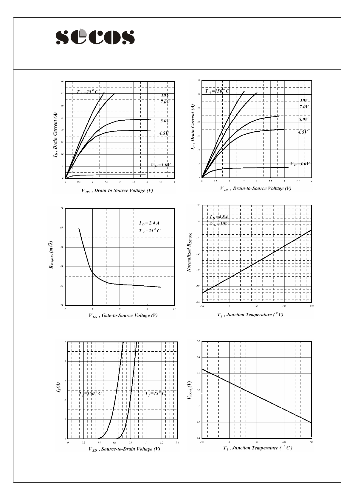
Characteristics Curve
Fig 1. Typical Output Characteristics
5.5A, 30V,RDS(ON) 45m
Ω
N-Channel Enhancement Mode Power Mos.FET
Fig 2. Typical Output Characteristics
Fig 3. On-Resistance v.s. Gate Voltage
Fig 4. Normalized On-Resistance
v.s. Junction Temperature
http://www.SeCoSGmbH.com/
01-Jun-2002 Rev. A
Fig 5. Forward Characteristics of
Reverse Diode
Fig 6. Gate Threshold Voltage v.s.
Junction Temperature
Any changing of specification will not be informed individual
Page3 of 4
Page 4
STT2604
5.5A, 30V,RDS(ON) 45m
Ω
Elektronische Bauelemente
N-Channel Enhancement Mode Power Mos.FET
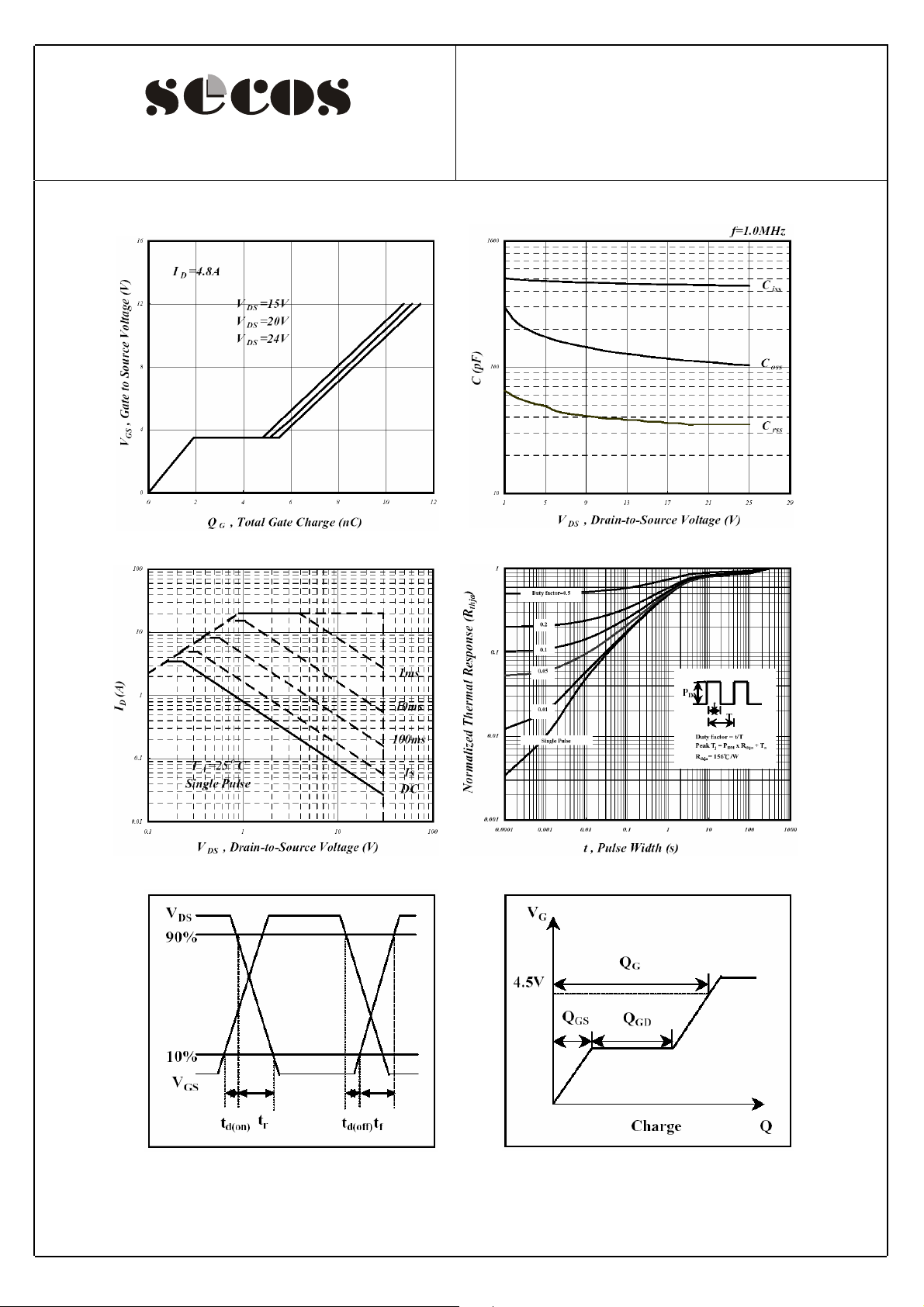
Fig 7. Gate Charge Characteristics Fig 8. Typical Capacitance Characteristics
Fig 9. Maximum Safe Operating Area Fig 10. Effective Transient Thermal Impedance
Fig 11. Switching Time Waveform Fig 12. Gate Charge Waveform
http://www.SeCoSGmbH.com/
01-Jun-2002 Rev. A
Any changing of specification will not be informed individual
Page 4 of 4
 Loading...