

Page 1
STT1NF100
N-CHANNEL 100V - 0.7Ω -1ASOT23-6L
STripFET™ II POWER MOSFET
PRELIMINARY DATA
TYPE V
DSS
R
DS(on)
I
D
STT1NF100 100V <0.8Ω 1A
■ TYPICAL R
■ EXCEPTIONAL dv/dt CAPABILITY
■ VERY LOW Qg
DS(on)
=0.7Ω
DESCRIPTION
This Power MOSFET is the latest development of STMicroelectronics unique “Single Feature Size
™”strip-
based process. The resulting transistor shows extremely high packing density for low on-resistance,
rugged avalance charac teristics and less critical alignment steps therefore a remarkable manufacturing reproducibility.
APPLICATIONS
■ DC-DC & DC-AC CONVERTERS
■ DC MOTOR CONTROL (DISK DRIV ES, etc.)
■ SYNCHRONOUS RECTIFICATION
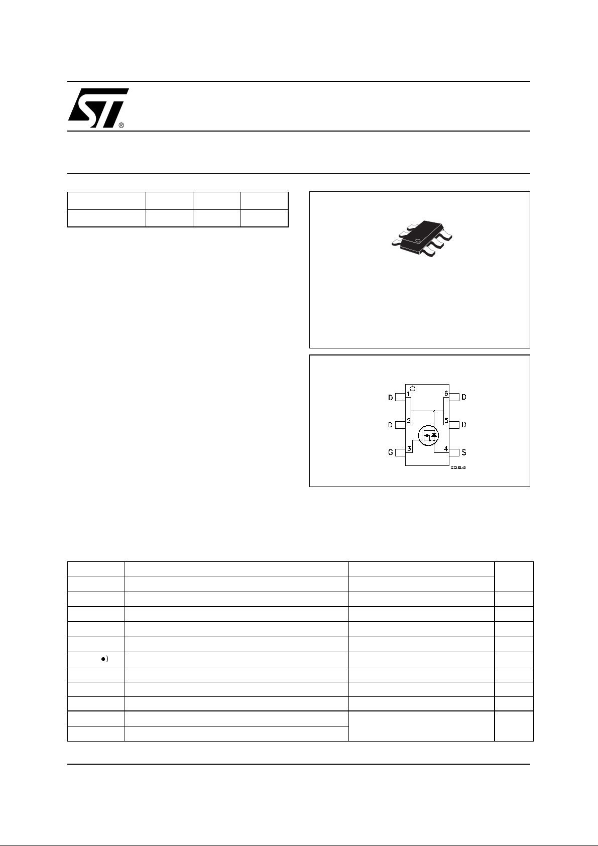
SOT23-6L
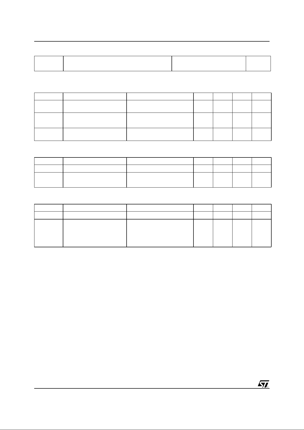
INTERNAL SCHEMATIC DIAGRAM
MARKING
■ STQ0
ABSOLUTE MAXIMUM RATINGS
Symbol Parameter Value Unit
V
DS
V
DGR
V
GS
I
D
I
D
I
DM
P
TOT
dv/dt(1) Peak Diode Recovery voltage slope 20 V/ns
T
stg
T
j
(●) Pulse width limited by safe operating area
September 2002
Drain-source Voltage (VGS=0)
Drain-gate Voltage (RGS=20kΩ)
100 V
100 V
Gate- source Voltage ± 20 V
Drain Current (continuous) at TC= 25°C
Drain Current (continuous) at TC= 100°C
()
Drain Current (pulsed) 4 A
Total Dissipation at TC= 25°C
1A
0.6 A
1.6 W
Derating Factor 0.013 W/°C
Storage Temperature
Max. Operating Junction Temperature
(1) ISD≤1A, di/dt ≤350A/µs, VDD≤ V
–55to150 °C
(BR)DSS,Tj≤TJMAX.
1/6
Page 2
STT1NF100
THERMAL DATA
Rthj-amb(*) Thermal Resistance Junction-ambient Max 78 °C/W
T
l
(*) When mounted on FR-4 board of 1inch² pad, 0.5oz Cu
ELECTRICAL CHARACTERISTICS (TCASE = 25 °C UNLES S OTHERWISE SPECIFIED)
OFF
Symbol Parameter Test Conditions Min. Typ. Max. Unit
V
(BR)DSS
I
DSS
I
GSS
ON (1)
Symbol Parameter Test Conditions Min. Typ. Max. Unit
V
GS(th)
R
DS(on)
Maximum Lead Temperature For Soldering Purpose 260 °C
Drain-source
ID= 250 µA, VGS= 0 100 V
Breakdown Voltage
Zero Gate Voltage
Drain Current (V
GS
=0)
Gate-body Leakage
Current (V
DS
=0)
Gate Threshold Voltage
Static Drain-source On
V
= Max Rating
DS
VDS= Max Rating, TC= 125 °C
V
= ± 20V ±100 nA
GS
V
DS=VGS,ID
=10V,ID= 0.5 A
V
GS
= 250µA
2V
0.7 0.8 Ω
1µA
10 µA
Resistance
DYNAMIC
Symbol Parameter Test Conditions Min. Typ. Max. Unit
(1) Forward Transconductance VDS=15V,ID=1A 1 S
g
fs
C
iss
C
oss
C
rss
Input Capacitance
Output Capacitance 20 pF
Reverse Transfer
Capacitance
V
=25V,f=1MHz,VGS=0
DS
105 pF
9pF
2/6
Page 3

STT1NF100
ELECTRICAL CHARACTERISTICS (CONTINUED)
SWITCHING ON
Symbol Parameter Test Conditions Min. Typ. Max. Unit
V
t
d(on)
t
r
Q
g
Q
gs
Q
gd
Turn-on Delay Time
Rise Time 5.5 ns
Total Gate Charge
Gate-Source Charge
Gate-Drain Charge
SWITCHING OFF
Symbol Parameter Test Conditions Min. Typ. Max. Unit
t
d(off)
t
f
Turn-off-Delay Time
Fall Time
SOURCE DRAIN DIODE
Symbol Parameter Test Conditions Min. Typ. Max. Unit
I
SD
I
SDM
V
SD
t
rr
Q
rr
I
RRM
Note: 1. Pulsed: Pulse duration = 300 µs, duty cycle 1.5 %.
2. Pulse width limited by safe operating area.
Source-drain Current 1 A
(2)
Source-drain Current (pulsed) 4 A
(1)
Forward On Voltage
Reverse Recovery Time
Reverse Recovery Charge
Reverse Recovery Current
=50V,ID= 0.5A
DD
= 4.7Ω VGS=10V
R
G
(see test circuit, Figure 1)
VDD=50V,ID=1A,
V
=10V
GS
(see test circuit, Figure 2)
VDD= 50V, ID= 0.5A,
=4.7Ω, VGS= 10V
R
G
(see test circuit, Figure 1)
ISD= 1A, VGS=0
= 1A, di/dt = 100A/µs,
I
SD
=20V,Tj= 150°C
V
DD
(see test circuit, Figure 3)
4ns
4
6
1
1.5
13
6.5
1.2 V
45
60
2.7
nC
nC
nC
ns
ns
ns
nC
A
3/6
Page 4

STT1NF100
Resistive Loa d
Fig. 3: Test Circuit For Diode Recovery Behaviour
Fig. 2: Gate Charge test CircuitFig. 1: Switching Times Test Circuit For
4/6
Page 5

TSOP-6 MECHANICAL DATA
STT1NF100
DIM.
MIN. TYP. MAX. MIN. TYP. MAX.
A 0.90 1.45 0.035 0.057
A1 0.00 0.15 0.000 0.006
A2 0.90 1.30 0.035 0.051
b 0.25 0.50 0.010 0.020
C 0.09 0.20 0.004 0.008
D 2.80 3.10 0.110 0.122
E 2.60 3.00 0.102 0.118
E1 1.50 1.75 0.059 0.069
L 0.35 0.55 0.014 0.022
e 0.95 0.037
e1 1.90 0.075
mm mils
AA2
A1
b
e
c
L
E
e1
D
E1
5/6
Page 6

STT1NF100
Information furnished is believed to be accurate and reliable. However, STMicroelectronics assumes no responsibility for t he
consequences of use of su ch in formation nor for any in fringement of paten ts or o ther rights of third parties w hich may result from
its use. No license is granted by implication or otherwise under any patent or patent rights of STMicroelectronics. Specifications
mentioned in this publication are subject to change without notice. This publication supersedes and replaces all information
previously suppli ed. STMi croelect ronics pr oducts are not author ized for use as c ritical component s in li fe suppo rt devi ces or
systems without express written approval of STMicroelectronics.
Australia - Brazil - Canada - China - Finland - France - Germany - Hong Kong - India - Israel - Italy - Japan - Malaysia - Malta - Morocco
© The ST logo is a registered trademark of STMicroelectronics
© 2002 STMicroelectronics - Printed in Italy - All Rights Reserved
Singapore - Spain - Sweden - Switzerland - United Kingdom - United States.
STMicroelectronics GROUP OF COMPANIES
© http://www.st.com
6/6
 Loading...