

Page 1
1/12June 2003
■ SUPPLY VOLTAGE RANGE: 4V TO 5.5V
■ TYPICAL PEAK OUTPUT CURRENT:
(SOURCE 2A, SINK 3.5A)
■ OPERATING FREQUENCY: 30 TO 750 KHz
■ SMART TURN-OFF ANTICIPATION TIMING
■ AUTOMATICTURN OFF FOR DUTY CYCLE
LESS THAN 14%
■ POSSIBILITY TO OPERATEIN
DISCONTINUOUS MODE
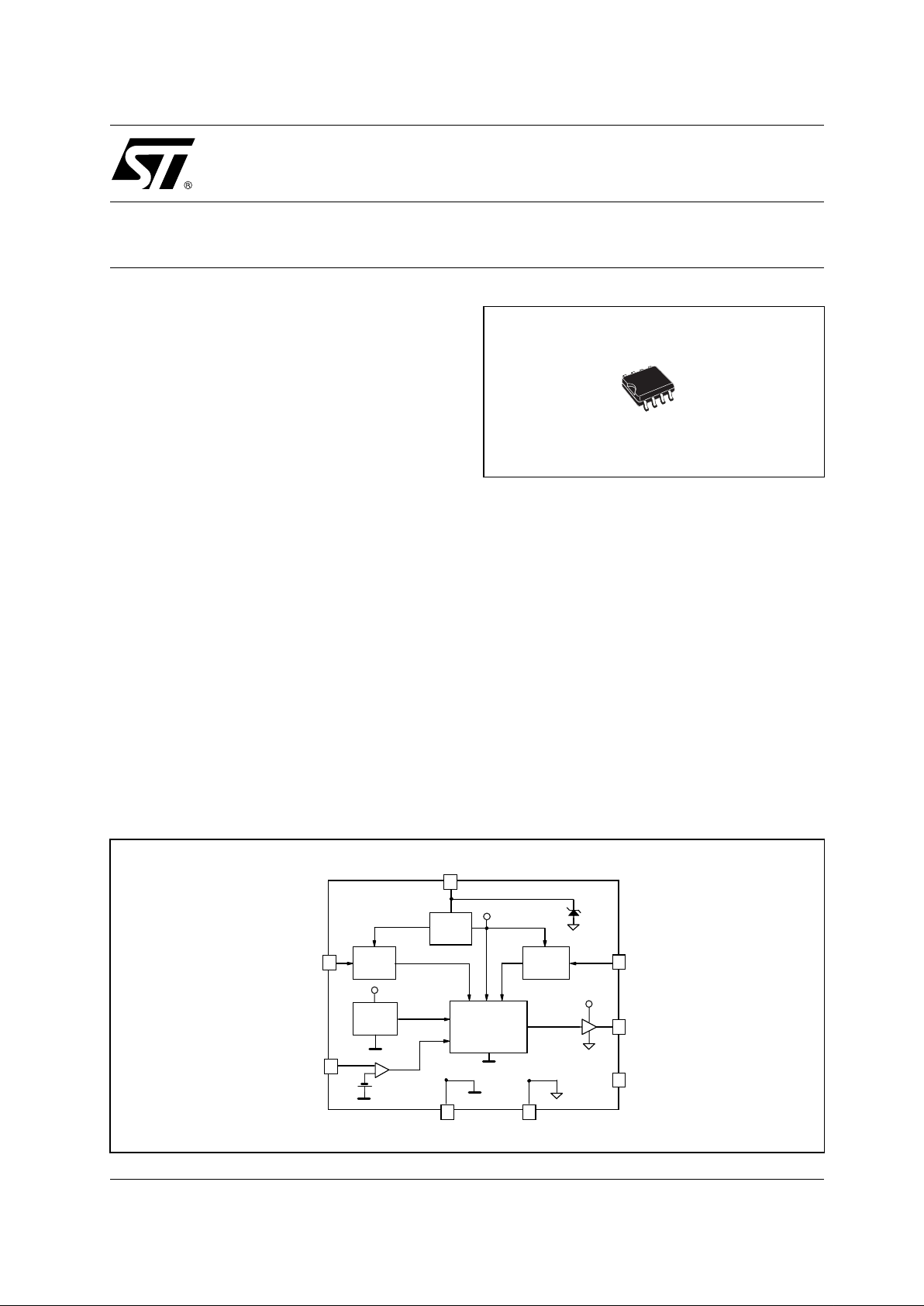
DESCRIPTION
STSR3 Smart Driver IC provides a high current
outputs to properly drive secondary Power
Mosfets used as Synchronous Rectifier in low
output voltage, high efficiency Flyback
Converters. From a synchronizing clock input,
withdrawn on the secondary side of the isolation
transformer, the IC generates a drivi ng s ignal with
set dead time s with respect to the primary side
PWM signal .
The IC operation prevents secondary side
shoot-through conditions at t urn-on of the primary
switch providing anticipation in turn-off the output.
This sm art function is implemented by a fast
cycle-after-cycle logic control mechanism, based
on a high frequency oscillator synchronized by the
clock signal. This anticipation is externally set
through external component. A special Inhibit
function allows to shut-off the drive output. This
feature make s discontinuous conducti on mode
possible and avoids reverse conduction of the
synchronous rectifier.
STSR3
SYNCHRONOUS RECTIFIERS
SMART DRIVER FOR FLYBACK
PEAK
DETECTOR
BIAS
UVLO
CK
Vcc
6
5.7V
8
4
2
OUTPUT
BUFFER
1
N/C
PWRGND
SGLGND
ANTICIPATION
SET
3
5
INHIBIT
25mV
+
DIGITAL
CONTROL
HIGH
FREQUENCY
OSCILLATOR
7
+
+
+
OUT
GATE
SETANT
SCHEMATIC DIAGRAM
SO-8
Page 2
STSR3
2/12
ABSOLUTE MAXIMUM RATINGS
Absolute Maximum Ratings are those values beyond which damage to the device may occur. Functional operation under these condition is
not implied.
(*) A higher positive voltage level can be applied to the pin with a resistor which limits the current flowing into the pin to 10mA maximum
THERMAL DATA
(*) This value is referred to one layer pcb board with minimum copper connections for the leads. a minimum value of 120 °C/W can be
obtained improving thermal conductivity of the board
ORDERING CODES
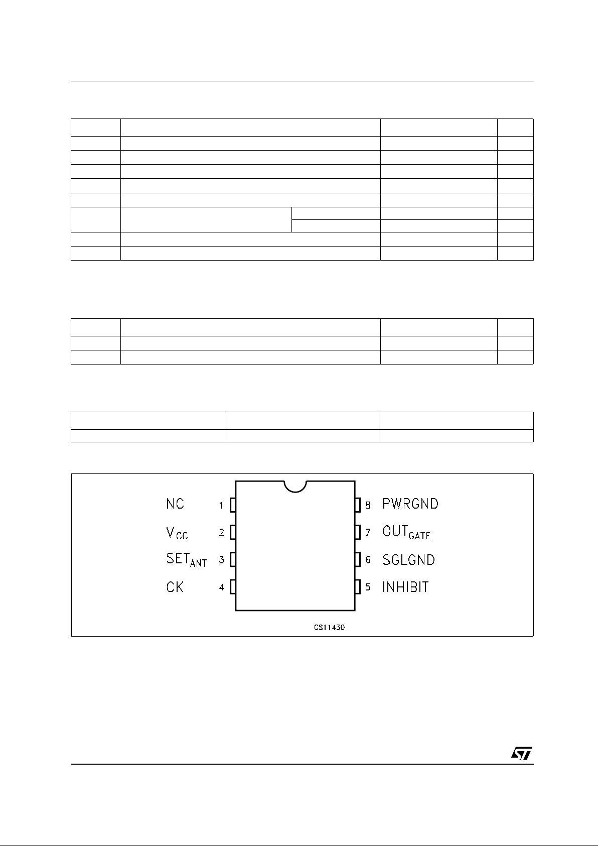
CONNECTION DIAGRAM (top view)
Symbol Parameter Value Unit
V
CC
DC Input Voltage
-0.3 to 6 V
V
OUTGATE
Max Gate Drive Output Voltage -0.3 to V
CC
V
V
INHIBIT
Max INHIBIT Voltage (*) -0.6 to V
CC
V
V
CK
Clock Input Voltage Range (*) -0.3 to V
CC
V
P
TOT
Continuous Power Dissipation at TA=105°C without heatsink 270 mW
ESD Human Body Model Pins 1,2, 4, 5, 6, 7, 8 ±1KV
Pin 3 ±0.9 KV
T
stg
Storage Temperature Range
-55 to +150 °C
T
op
Operating Junction Temperature Range -40 to +125 °C
Symbol Parameter SO-8 Unit
R
thj-amb
Thermal Resistance Junction-case
40 °C/W
R
thj-amb
Thermal Resistance Junction-ambient (*)
160 °C/W
TYPE SO-8 SO-8 (T&R)
STSR3 STSR3CD STSR3CD-TR
Page 3
STSR3
3/12
PIN DESCRIPTION
Pin N° Symbol Name and Function
1 NC No internally connected
2V
CC
The supply voltage range from 4.0V to 5.5V allows applications with logic gate
threshold mosfets. UVLO feature guarantees proper start-up while it avoids
undesirable driving during eventual dropping of the supply voltage.
3 SET
ANT
The voltage on this pin sets the anticipation (t
ANT
) in turning off the OUT
GATE
It is
possible to choose among three different anticipation times by discrete
partitioning of the supply voltage.
4 CK This input provides synchronization for IC’s operations, being the transitions
between the two output conditions based on a positive threshold, equal for the
two slopes. A smart internal control logic mechanism using a 15MHz internal
oscillator generates proper anticipation timing at the turn-off of each output. This
feature allows safe turn-off of Synchronous Rectifier avoiding any eventual
shoot-through situation on secondary side at both transitions. Smart clock
revelation mechanism makes these operations independent by false triggering
pulses generated in light load conditions. Absolute maximum voltage rating of the
pin can be exceeded limiting the current flowing into the pin to 10mA max.
5 INHIBIT This input enables OUT
GATE
to work when its voltage is lower than the negative
threshold voltage (V
INHIBIT<VH
). If V
INHIBIT>VH
the OUT
GATE
will be high for a
minimum conduction time (t
ON(GATE)
). In typical flyback converter application, it is
possible to turn off the synchronous MOSFET when the current through it tends to
reverse, allowing discontinuous conduction mode and providing protection to the
converter from eventual sinking current from the load.Absolute maximum voltage
rating of the pin can be exceeded limiting the current flowing into the pin to 10mA
max.
6 SGLGND Reference for all the control logic signals. This pin is completely separated from
the PWRGND to prevent eventual disturbances to affect the control logic.
7OUT
GATE
Gate Drive signal for synchronous MOSFET. Anticipation [t
ANT
] in turning off
OUT
GATE
is provided during the transition in which the clock input goes to high
level.
8 PWRGND Reference for power signals, this pin carries the full peak currents for the two
outputs.
Page 4
STSR3
4/12
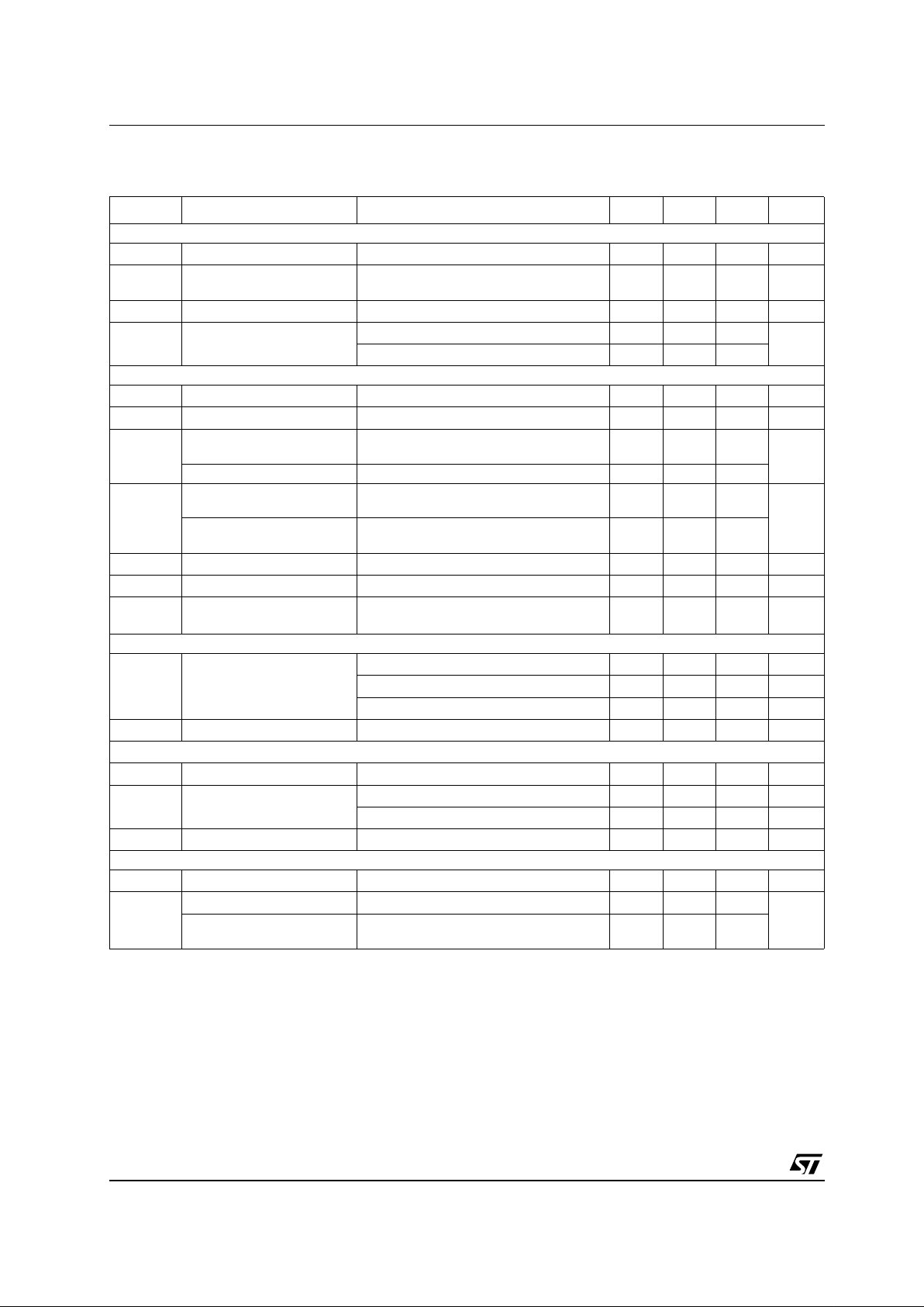
ELECTRICAL CHARACTERISTICS(VCC=5V, CK= 250kHz, duty -c ycle =50%, V
INHIBIT
=-200mV, TJ=-40
to 125°C, unles s otherwise specified.)
Note1:tRis measured between 10% and 90% of the final voltage; tFis measuredbetween 90%and 10% on theinitialvoltage
Note2: Parameter guaranteed by design
Symbol Parameter Test Conditions Min. Typ. Max. Unit
SUPPLY INPUT AND UNDER VOLTAGE LOCK OUT
V
CCON
Start Threshold 3.8 4 V
V
CCOFF
Turn OFF Threshold After
Start
3.5 3.6 V
V
Z
Zener Voltage CK=0V IZ= 2mA 5.5 5.8 6 V
I
CC
Unloaded Supply Current OUT
GATE
= no load 15 20 mA
CK=0V OUT
GATE
= no load 3 5
GATE DRIVER OUTPUTS
V
OL
Output Low Voltage I
OUTGATE
=-200mA 0.10 0.16 V
V
OH
Output High Voltage I
OUTGATE
=200mA 4.70 4.85 V
I
OUT
Output Source Peak
Current
2A
Output Sink Peak Current 3.5
R
OUT
Output Series Source
Resistance
I
OUTGATE
=-200mA 0.75 1.5 Ω
Output Series Sink
Resistance
I
OUTGATE
=200mA 0.5 0.8
t
R
OUT
GATE
Rise Time C
LOAD
=5nF (Note 1) 40 ns
t
F
OUT
GATE
Fall Time C
LOAD
=5nF (Note 1) 30 ns
t
P
Clock Propagation Delay to
Turn ON of OUT
GATE
No Load 50 ns
TURN-OFF ANTICIPATION TIME
t
ANT
OUT
GATE
Turn-off
Anticipation Time
V
ANT
= 0 to 1/3VCC; no load 75 ns
V
ANT
= 1/3VCCto 2/3VCC; no load 150
V
ANT
= 2/3VCCto VCC; no load 225
I
SETANT
Leakage Current (Note 2) -0.1 0.1 µA
INHIBIT OUT
GATE
ENABLE
V
H
Threshold Voltage TJ= 25°C -30 -25 mV
I
H
Leakage Current (Note 2) V
INHIBIT
= 200mV -400 nA
V
INHIBIT
= -200mV 1 µA
t
ON(GATE)
Minimum OUT
GATE
On time V
INHIBIT
= +200mV 250 ns
SYNCHRONIZATION INPUT
V
CK
Reference Voltage TJ= 25°C 2.6 2.8 V
D
OFF
Duty Cycle Shut Down TJ= 25°C 13 14 %
Duty Cycle Turn ON after
Shut Down
T
J
= 25°C 18 20
Page 5

STSR3
5/12
TIMING DIAGRAM
APPLICATION INFORMATION: STSR3 IN FLYBACK CONVERTER SE CONDARY SIDE
NOTES
1) Ceramic Capacitors C1 and C2 must be placed very close to the IC;
2)R1andR2settheanticipationtimebypartitioningtheV
CC
voltage;
3) R3 and R4 is a resistor divider meant to provide the correct CK voltage range;
4) R5 limits the current flowing through diode D2 when Freewheeling drain voltage is high;
5) D1 could be necessary to protect INHIBIT pin from negative voltages.
6) D2 could be necessary to protect INHIBIT pin from voltages higher than V
CC
7) D3 could be necessary to protect CK pin from voltages higher than VCC.
8) SGLGND layout trace must not include OUT
GATE
current paths.
9) A capacitor in parallel with R4 could be necessary to eliminate turn off voltage spike.
+5V
+5V
VoutVin
+5V
Cout
C2
100nF
R1
R2
R3
R4
D1
D2
C1
100nF
R5
STSR3
4
5
7
8
2
6
3
Ck
INHIBIT
OUTGate
PWRGND
Vcc
SGLGND
SETANT
TRANSFORMER
MosfetN
D3
PWM
Feedback
Loop
option
Page 6

STSR3
6/12
EXAMPLE OF COMPONENTS S ELECTION FOR A FLYBACK CONVERTER
Flyback Specification:
V
IN
=36-72V
V
OUT
=3.3V
n=Np/Ns=4.5
R
3
and R4are calculated assuring a minimum voltage of 2.8V at Ck pin. At 36V input, t he voltage on the
secondary winding is 36/4.5=8V. Choosing R
3
=1.5KΩ,R4results to be:
R
4
=1kΩ is cho se n. At 72V input the current at Ck pin is calculated as:
This v alue is below the maximum allowabl e current flowing into the Ck pin (10mA). If the 10mA value is
exceeded an external diode co nnec ted to V
CC
must be added (D3).
R
1
and R2values set the anticipation time for OUT
GATE
.ForR1=∞and R2=0, t
ANT
=75ns; for
R
1=R2
=10kΩ,t
ANT
=150ns; for R1=0 and R2=∞,t
ANT
=225ns.
The RC group composed by R
5
and the parasitic capacitance of Inhibit pin (typically 5pF) delays the
signal on Inhibit comparator. Th is d elay must be lower than 200ns. This condition imposes a maximum
value for R
5
of about 20kΩ.
In general a suggested value for R
5
is 10kΩ. At 72V input, the secondary voltage is 16V, so the maximum
current flowing int o Inhibit pin is 16V /10kΩ=1.6mA which is below the maximum allowable cu rren t for the
pin (10mA). If the 10mA value is exceeded an external di ode (D2) connected to V
CC
must be added.
The maximum negative voltage of –0.6V must be guaranteed for the Inhibit pin. If this negative vol tage is
exceeded the current must be limited to 50mA. If necessary, a diode (D1) connected to SGLGND can be
added to satisfy this specification.
R
4
V
CKR3
×
V
INICK 2.8()
– R3V
CK
–×
--------------------------------------------------------------- -
≥ 1kΩ
2.8V 1.5kΩ×
8V 220µA– 1.5kΩ 2.8V–×
------------------------------------------------------------------------- -
× 862Ω==
I
CK
V
IN max()
V
CC
– 0.3–
R
3
-----------------------------------------------------
16 5– 0.3–
1.5kΩ
----------------------------- -
7.13mA===
Page 7

STSR3
7/12
INHIBIT O P ERATION OF OUT
GATE
IN DIS CONTINUOUS CONDUCTION MODE
INHIBIT O P ERATION OF OUT
GATE
Page 8

STSR3
8/12
TYPICAL PERFORMANCE CHARACTE RISTICS (unless otherwise specified Tj=25°C
Figure1 : Zener Characteristics
Figure2 : Ris e and Fall Time vs Load Capacitor
Figure3 : OUT
GATE
vs Characteristics
Figure4 : Sink-Source ON Resistance vs
Temperature
Figure5 : Clock Threshold Voltage vs
Temperature
Figure6 : INHI B IT Threshold Voltage vs
Temperature
Page 9

STSR3
9/12
Figure7 : Supply Current vs Load Cap ac itor
Figure8 : Supply Current vs Clock Frequency
Figure9 : G ATE ON Time vs Temperature
Figure10 : Duty Cycle Shu t Down vs
Temperature
Figure11 : Duty Cycle Turn ON After Shut Down
vs Temperature
Figure12 : Clock Leakage Current vs Clock
Voltage
Page 10

STSR3
10/12
DIM.
mm. inch
MIN. TYP MAX. MIN. TYP. MAX.
A 1.35 1.75 0.053 0.069
A1 0.10 0.25 0.04 0.010
A2 1.10 1.65 0.043 0.065
B 0.33 0.51 0.013 0.020
C 0.19 0.25 0.007 0.010
D 4.80 5.00 0.189 0.197
E 3.80 4.00 0.150 0.157
e 1.27 0.050
H 5.80 6.20 0.228 0.244
h 0.25 0.50 0.010 0.020
L 0.40 1.27 0.016 0.050
k ˚ (max.)
ddd 0.1 0.04
SO-8 MECHANICAL DATA
0016023/C
8
Page 11

STSR3
11/12
DIM.
mm. inch
MIN. TYP MAX. MIN. TYP. MAX.
A 330 12.992
C 12.8 13.2 0.504 0.519
D 20.2 0.795
N 60 2.362
T 22.4 0.882
Ao 8.1 8.5 0.319 0.335
Bo 5.5 5.9 0.216 0.232
Ko 2.1 2.3 0.082 0.090
Po 3.9 4.1 0.153 0.161
P 7.9 8.1 0.311 0.319
Tape & Reel SO-8 MECHANICAL DATA
Page 12

STSR3
12/12
Information furnished is believed to be accurate and reliable. However, STMicroelectronics assumes no responsibility for the
consequences of use o f suc h inf ormat ion n or f or an y infr ingeme nt of paten ts or oth er ri gh ts of third part ies whic h may resul t f rom
its use. No license is granted by implication or otherwise under any patent or patent rights of STMicroelectronics. Specifications
mentioned in this publication are subject to change without notice. This publication supersedes and replaces all information
previously supplied. STMicroelectronics products are not authorized for use as critical components in life support devices or
systems without express written approval of STMicroelectronics.
© The ST logo is a registered trademark of STMicroelectronics
© 2003 STMicroelectronics - Printed in Italy - All Rights Reserved
STMicroelectronics GROUP OF COMPANIES
Australia - Brazil - Canada - China - Finland - France - Germany - Hong Kong - India - Israel - Italy - Japan - Malaysia - Malta - Morocco
Singapore - Spain - Sweden - Switzerland - United Kingdom - United States.
© http://www.st.com
 Loading...