

Page 1
®
HIGH EFFICIENCY SWITCHED MODE RECTIFIER
MAIN PRODUCT CHARACTERISTI CS
STSR220
I
F(AV)
V
RRM
(max) 0.8V
V
F
2A
200V
FEATURES AND BENE FITS
VERY LOW CO NDU CT ION LOSS E S
NEGLIGIBLE SWITCHING LOSSE S
LOW FORWARD AND REVERSE RECOVERY
TIMES
HIGH SURGE CURRENT
DESCRIPTION
Low voltage drop rectifiers suited for Switched
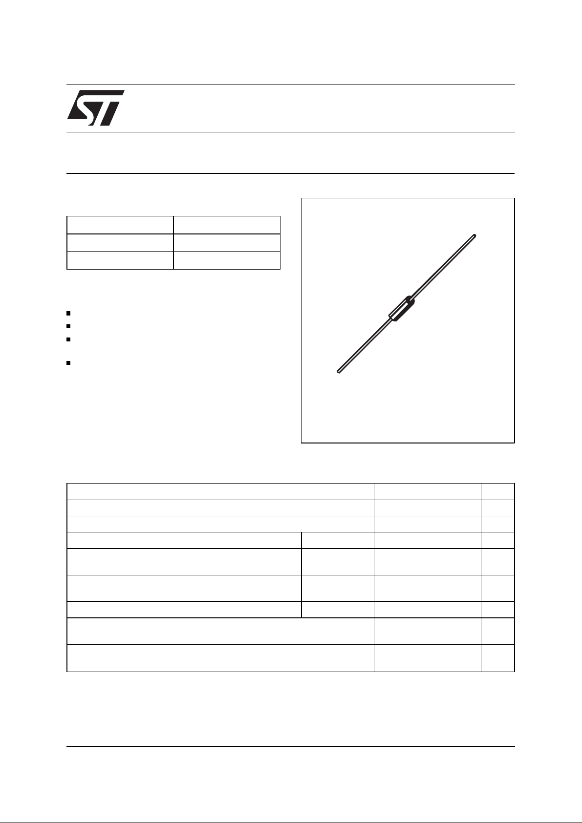
F126
(Plastic)
Mode Power Supplies and for switching mode
base drive and transistor circuit.
ABSOLUTE RATINGS
(limiting values)
Symbol Parameter Value Unit
V
RRM
V
RSM
I
FRM
I
F (AV)
I
FSM
Repetitive peak reverse voltage
200 V
Non repetitive peak reverse voltage 220 V
Repetive peak forward current tp < 20µs70A
Average forward current * Ta = 75°C
δ
= 0.5
Surge non repetitive forward current tp = 10ms
2A
70 A
Sinusoidal
P
tot
T
stg
T
T
L
Power dissipation * Ta = 75°C 1.85 W
Storage temperature range
Maximum junction temperature
j
Maximum lead temperature for soldering during 10s at
- 40 to + 150
150
230 °C
4mm from case
°C
* On infinite heatsink with 10mm lead length
October 1999 - Ed: 2A
1/3
Page 2
STSR220
THERMAL RESISTANCE
Symbol Parameter Value Unit
R
th (j - a)
* On infinite heatsink with 10mm lead lengh.
Junction to ambient thermal resistance *
40 °C/W
STATIC ELECTRICAL CHARACTE RISTICS
Symbol Parameter Test Conditions Min. Typ. Max. Unit
I
R
Reverse leakage
VR = V
RRM
Tj = 25°C 10
current
T
= 100°C 0.5 mA
j
V
F
Forward voltage
IF = 2A Tj = 25°C 1 V
drop
= 2A Tj = 100°C 0.8
I
F
RECOVERY CHARA CTERISTICS
Symbol Test Conditions Min. Typ. Max. Unit
t
rr
Tj = 25°C IF = 1A
= 30V
V
R
di
/dt = -50A/µs35ns
F
µ
A
Q
rr
t
fr
Tj = 25°C IF = 2A
< 30V
V
R
Tj = 25°C IF = 1A
Measured at 1.1x V
V
FP
Tj = 25°C IF = 1A tr = 10ns 5 V
F
di
/dt = -20A/µs12nC
F
tr = 10ns 20 ns
To evaluate the conduction losses use the following equation:
P = 0.68 x I
F(AV)
+ 0.06 I
F2(RMS)
2/3
Page 3

PACKAGE ME CHANICAL D AT A
F126 (Plastic)
STSR220
D
DIMENSIONS
REF.
A 6.05 6.20 6.35 0.238 0.244 0.250
B 2.95 3.00 3.05 0.116 0.118 0.120
C 26 31 1.024 1.220
Millimeters Inches
Min. Typ. Max. Min. Typ. Max.
A
CC
D
B
D 0.76 0.81 0.86 0.030 0.032 0.034
Marking
: type number; ring at cathode end
Cooling method: by convection (method A)
Weight: 0.4 g
Information furnished is believed to be accurate and reliable. However, STMicroelectronics assumes no responsibility for the consequences of
use of such information nor for any infringement of patents or other rights of third parties which may result from its use. No license is granted by
implication or otherwis e under any patent or patent rights of STMicroelec tronics. Specifications menti oned in this publication are subject to
change without notice. This publication supersedes and replaces all information previously supplied.
STMicroelectronics products ar e not authorized for use as critical c omponents in life support devices or systems without expres s w ri tte n approval of STMicroelectronics.
The ST logo is a registered trad emark of STMicroelectr onics
© 1999 STMicroelectronics - Printed in Italy - All rights reserved.
STMicroelectronics GROUP OF COMPANIES
Australia - Brazil - China - Finland - France - Germany - Hong Kong - India - Italy - Japan - Malaysia
Malta - Morocco - Singapore - Spain - Sweden - Switzerland - United Kingdom - U.S.A.
http://www.st.com
3/3
 Loading...