

Page 1
STSJ3NM50
N-CHANNEL 500V - 2.5Ω - 3A PowerSO-8
Zener-Protected MDmesh™ POWER MOSFET
TYPE V
STSJ3NM50 500 V < 3 Ω 3 A
■ TYPICAL R
■ HIGH dv/dt AND AVALANCHE CAPABILITIES
■ IMPROVED ESD CAPABILITY
■ LOW INPUT CAPACITANCE AND GATE
DS
DSS
(on) = 2.5 Ω
R
DS(on)
I
D
CHARGE
■ LOW GATE INPUT RESIST ANC E
■ TIGHT PROCESS CONTROL AND HIGH
MANUFACTORING YIELDS
DESCRIPTION
The MDmesh™
is a new revolutionary MOSFET
technology that associates the Multiple Drain process with the Company’s PowerMESH™ horizontal
layout. The resulting product has an outstanding low
on-resistance, impressively high dv/dt and excellent
avalanche characteristics. The adoption of the
Company’s proprietary strip technique yields overall
dynamic performance that is significantly better than
that of similar completition’s products.
APPLICATIONS
The MDmesh™ family is very suitable for increase
the power density of high voltage converters allowing system miniaturization and higher efficiencies.
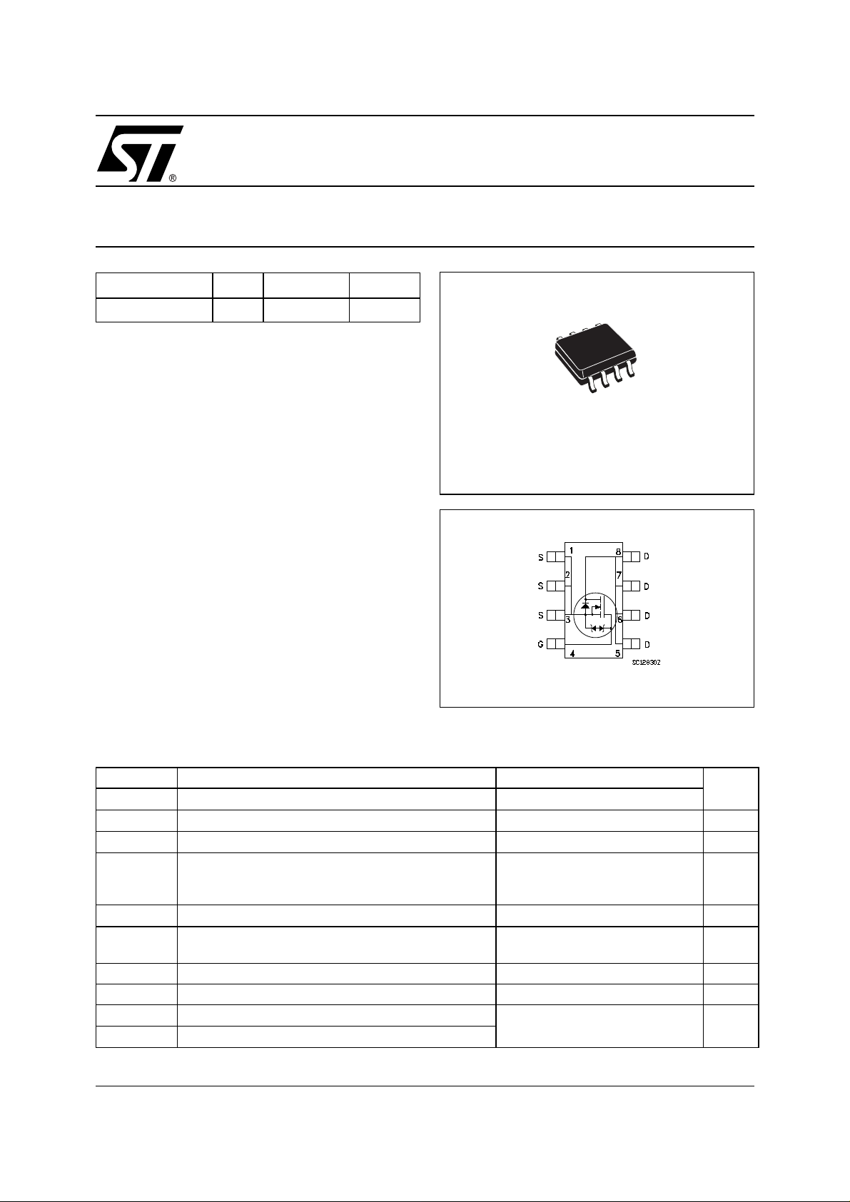
PowerSO-8
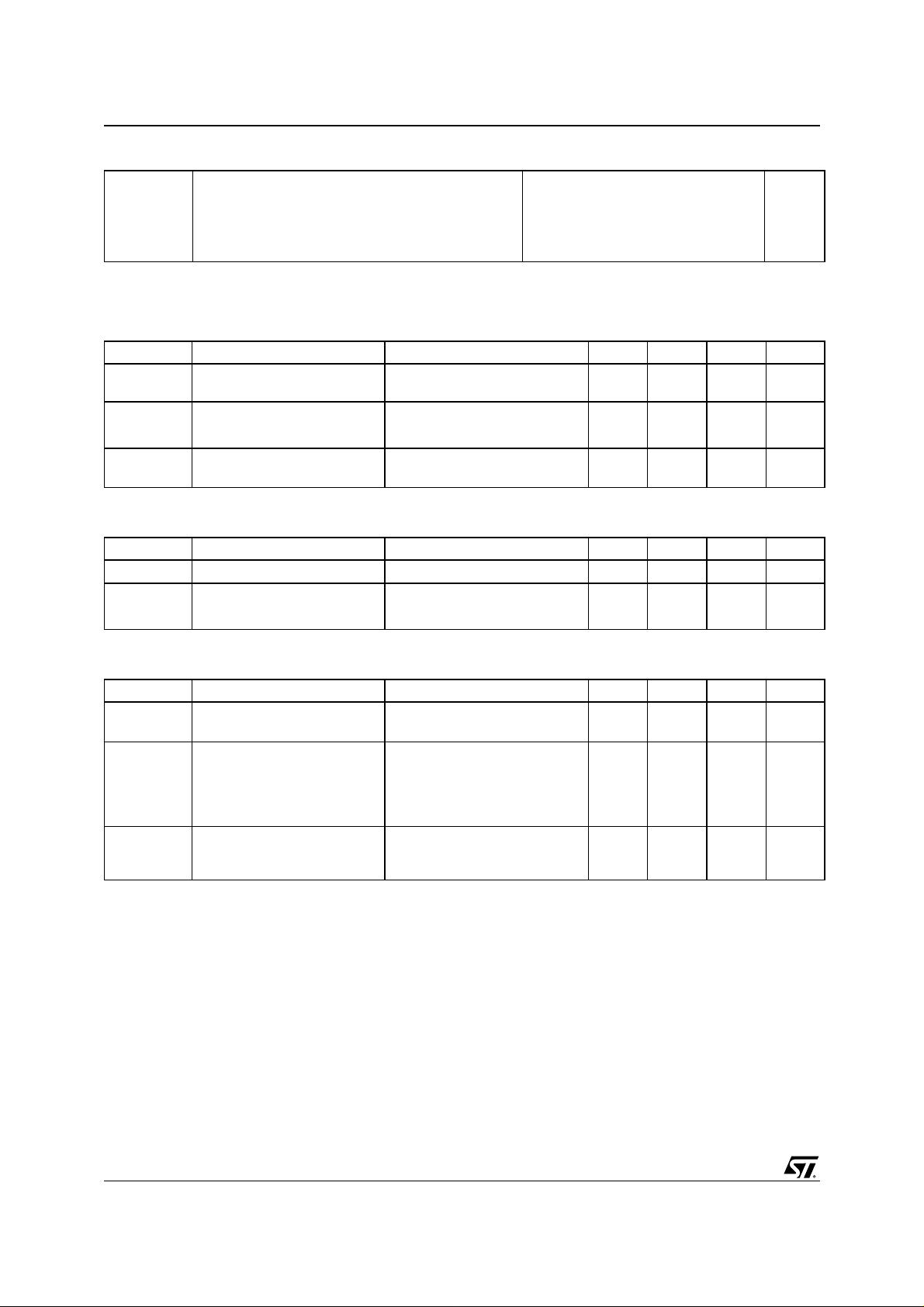
INTERNAL SCHEMATIC DIAGRAM
DRAIN CONTACT ALSO ON THE BACKSIDE
ABSOLUTE MAXIMUM RATINGS
Symbol Parameter Value Unit
V
DS
V
DGR
V
GS
I
D
I
DM
P
TOT
P
TOT
dv/dt (3) Peak Diode Recovery voltage slope 15 V/ns
T
stg
T
(2)
j
Drain-source Voltage (VGS = 0)
Drain-gate Voltage (RGS = 20 kΩ)
Gate- source Voltage ± 30 V
Drain Current (continuous) at TC = 25°C
Drain Current (continuous) at TA = 25°C (1)
Drain Current (continuous) at T
Drain Current (pulsed) 12 A
Total Dissipation at TC = 25°C
Total Dissipation at TA = 25°C (1)
Derating Factor (1) 0.02 W/°C
Storage Temperature
Max. Operating Junction Temperature
= 100°C
C
500 V
500 V
3
0.63
1.89
70
3
– 65 to 150 °C
A
A
A
W
W
1/8August 2002
Page 2
STSJ3NM50
THERMA L D ATA
Rthj-c Thermal Resistance Junction-case Max 1.78 °C/W
Rthj-amb Thermal Resistance Junction-ambient Max (1) 42 °C/W
T
T
stg
Max. Operating Junction Temperature 150 °C
j
Storage Temperature – 65 to 150 °C
ELECTRICAL CHARACTERISTICS (T
= 25 °C UNLESS OTHERWISE SPECIFIED)
CASE
OFF
Symbol Parameter Test Conditions Min. Typ. Max. Unit
V
(BR)DSS
Drain-source
ID = 1 mA, VGS = 0 500 V
Breakdown Voltage
V
= Max Rating
DS
VDS = Max Rating, TC = 125 °C
V
= ± 20V ±5 µA
GS
1µA
10 µA
ON
I
I
GSS
(1)
DSS
Zero Gate Voltage
Drain Current (V
GS
Gate-body Leakage
Current (V
DS
= 0)
= 0)
Symbol Parameter Test Conditions Min. Typ. Max. Unit
V
V
GS(th)
R
DS(on)
Gate Threshold Voltage
Static Drain-source On
= VGS, ID = 250µA
DS
VGS = 10 V, ID = 1.5 A
345V
2.5 3 Ω
Resistance
DYNAMIC
Symbol Parameter Test Conditions Min. Typ. Max. Unit
(4) Forward Transconductance VDS > I
g
fs
C
iss
C
oss
C
rss
Input Capacitance
Output Capacitance 40 pF
Reverse Transfer
Capacitance
R
G
Gate Input Resistance f=1 MHz Gate DC Bias = 0
ID= 3 A
V
DS
Test Signal Level = 20mV
Open Drain
x R
D(on)
DS(on)max,
= 25 V, f = 1 MHz, VGS = 0
0.7 S
140 pF
40 pF
4 Ω
2/8
Page 3
STSJ3NM50
ELECTRICAL CHARACTERISTICS (CONTINUED)
SWITCHING ON
Symbol Parameter Test Conditions Min. Typ. Max. Unit
V
t
d(on)
t
r
Q
g
Q
gs
Q
gd
Turn-on Delay Time
Rise Time 10 ns
Total Gate Charge
Gate-Source Charge
Gate-Drain Charge
SWITCHING OFF
Symbol Parameter Test Conditions Min. Typ. Max. Unit
t
r(Voff)
t
t
f
c
Off-Voltage Rise Time
Fall Time
Cross-Over Time
SOURCE DRAIN DIODE
Symbol Parameter Test Conditions Min. Typ. Max. Unit
I
SD
I
SDM
VSD (4)
t
rr
Q
rr
I
RRM
t
rr
Q
rr
I
RRM
Note: 1. When mounted on 1inch² FR4 Board, 2oz of Cu, t ≤ 10 sec.
2. Pulse width l i m i ted by safe oper ating area
3. I
4. Pulsed: Pu l se duration = 400 µs, duty cycl e 1.5 %
Source-drain Current 3 A
(2)
Source-drain Current (pulsed) 12 A
Forward On Voltage
Reverse Recovery Time
Reverse Recovery Charge
Reverse Recovery Current
Reverse Recovery Time
Reverse Recovery Charge
Reverse Recovery Current
<3.3A, di/dt<400A/µs, VDD<V
SD
(BR)DSS
, TJ<T
= 250 V, ID = 1.5 A
DD
R
= 4.7Ω VGS = 10 V
G
(see test circuit, Figure 3)
VDD = 400 V, ID = 3 A,
VGS = 10 V
= 480 V, ID = 3 A,
V
DD
RG=4.7Ω, V
GS
= 10 V
(see test circuit, Figure 3)
ISD = 3 A, VGS = 0
= 3, di/dt = 100A/µs,
I
SD
VDD = 100 V, Tj = 25°C
(see test circuit, Figure 5)
ISD = 3, di/dt = 100A/µs,
V
= 100 V, Tj = 150°C
DD
(see test circuit, Figure 5)
JMAX
7ns
5.5
2.5
2.4
8
9
15
1.5 V
210
790
7.5
282
1.1
7.7
nC
nC
nC
ns
ns
ns
ns
nC
A
ns
nC
A
GATE-SOURCE ZENER DIODE
Symbol Parameter Test Conditions Min. Typ. Max. Unit
BV
GSO
Gate-Source Breakdown
Igs=± 1mA (Open Drain) 30 V
Voltage
PROTECTION FEATURES OF GATE-TO-SOURCE ZENER DIODES
The built-in back-to-back Zener diodes have specif ically been designed to enhanc e not only t he dev ice’s
ESD capability, but also to make them safely absorb possible voltage transients that may occasionally be
applied from gate to source. In this respect the Zener voltage is approp riate to achieve an efficient and
cost-effective intervention to protect the device’s integrity. These integrated Zener diodes thus avoi d the
usage of external components.
3/8
Page 4

STSJ3NM50
Output Characteristics
Transfer Characteristics
Static Drain-source On ResistanceTransconductance
4/8
Capacitance VariationsGate Charge vs Gate-source Voltage
Page 5

STSJ3NM50
Normalized Gate Threshold Volta ge vs Temp. Normalized On Resistance vs Temperatur e
Normalized BVdss vs TemperatureSource-drain Diode Forward Characteristics
5/8
Page 6

STSJ3NM50
Fig. 2: Unclamped Inductive WaveformFig. 1: Unclamped Inductive Load Test Circuit
Fig. 3: Switching Times Test Circuit For
Resistive Load
Fig. 5: Test Circuit For Inductive Load Switching
And Diode Recovery Times
Fig. 4: Gate Charge test Circuit
6/8
Page 7

PowerSO-8™ MECHANICAL DATA
STSJ3NM50
DIM.
A 1.75 0.068
a1 0.1 0.25 0.003 0.009
a2 1.65 0.064
a3 0.65 0.85 0.025 0.033
b 0.35 0.48 0.013 0.018
b1 0.19 0.25 0.007 0.010
C 0.25 0.5 0.010 0.019
c1 45° (typ.)
D 4.8 5.0 0.188 0.196
E 5.8 6.2 0.228 0.244
e 1.27 0.050
e3 3.81 0.150
e4 2.79 0.110
F 3.8 4.0 0.14 0.157
L 0.4 1.27 0.015 0.050
M 0.6 0.023
S 8° (max.)
MIN. TYP MAX. MIN. TYP. MAX.
mm. inch
7/8
Page 8

STSJ3NM50
Information furnished is believed to be accurate and reliable. However, STMicroelectronics assumes no responsibility f or the
consequences of use of su ch in formation nor for any in fringement of paten ts or o ther rights of third parties w hich may result from
its use. No license is granted by implication or otherwise under any patent or patent rights of STMicroelectronics. Specifications
mentioned in this publication are subject to change without notice. This publication supersedes and replaces all information
previously suppli ed. STMi croelect ronics pr oducts are not author ized for use as c ritical component s in li fe suppo rt devi ces or
systems without express written approval of STMicroelectronics.
Australia - Brazil - Canada - China - Finland - France - Germany - Hong Kong - India - Israel - Italy - Japan - Malaysia - Malta - Morocco
© The ST logo is a registered trademark of STMicroelectronics
© 2002 STMicroelectronics - Printed in Italy - All Rights Reserved
Singapore - Spain - Sweden - Switzerland - United Kingdom - United States.
STMicroelectronics GROUP OF COMPANIES
© http://www.st.com
8/8
 Loading...