

Page 1
STSJ25NF3LL
N-CHANNEL 30V - 0.009Ω - 25A PowerSO-8™
LOW GATE CHARGE STripFET™ II POWER MOSFET
TYPE V
STSJ25NF3LL 30 V < 0.011 Ω 25 A
■ IMPROVED JUNCTION-CASE THERMAL
DSS
R
DS(on)
I
D
RESISTANCE
■ TYPICAL R
■ TYPICAL Q
■ CONDUCTION LOSSES REDUCED
■ SWITCHING LOSSES REDUCED
(on) = 0.009Ω
DS
= 21 nC
g
DESCRIPTION
This Power MOSFET is t he latest development of
STMicroelectronics unique “Single Feature Size
™”
strip-based process. This silicon, housed in thermally improved SO-8 package, exhibits optimal on-resistance versus gate charge trade-off plus lower
.
R
thj-c
APPLICATIONS
■ SPECIFICALLY DESIGNED AND OPTIMISED
FOR HIGH EFFICIENCY CPU CORE DC/DC
CONVERTERS FOR MOBILE PCs
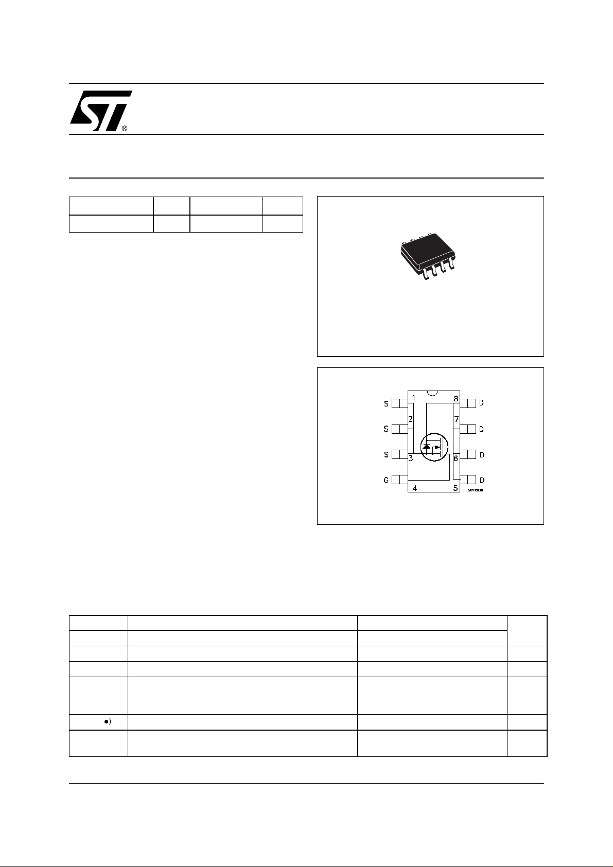
PowerSO-8
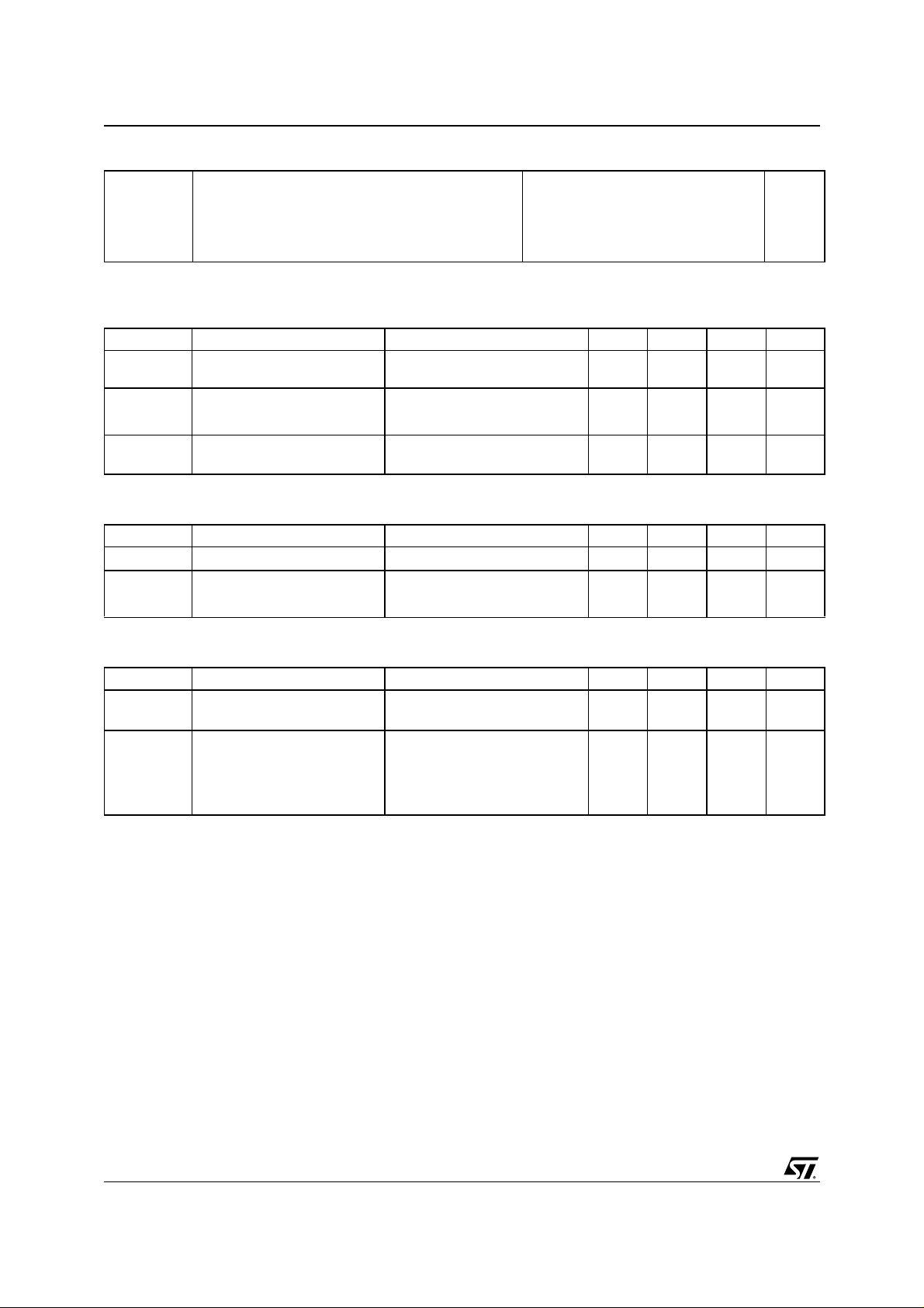
INTERNAL SCHEMATIC DIAGRAM
DRAIN CONTACT ALSO ON THE BACKSIDE
ABSOLUTE MAXIMUM RATINGS
Symbol Parameter Value Unit
V
DS
V
DGR
V
GS
I
D
I
DM
P
TOT
(●) Pulse width limited by safe operating area
Drain-source Voltage (VGS = 0)
Drain-gate Voltage (RGS = 20 kΩ)
Gate- source Voltage ± 16 V
Drain Current (continuous) at TC = 25°C (*)
Drain Current (continuous) at TA = 25°C (#)
Drain Current (continuous) at T
(l)
Drain Current (pulsed) 100 A
Total Dissipation at TC = 25°C
Total Dissipation at TA = 25°C (#)
= 100°C
C
(*)Value li m ited by wir es bonding
30 V
30 V
25
12
16
70
3
A
A
A
W
W
1/8March 2002
Page 2
STSJ25NF3LL
THERMA L D ATA
Rthj-c Thermal Resistance Junction-case Max 1.8 °C/W
Rthj-amb Thermal Resistance Junction-ambient Max (#) 42 °C/W
T
j
T
stg
(#) When mounted on 1inc h² FR4 Board, 2oz of Cu, t ≤ 10 sec.
Max. Operating Junction Temperature 150 °C
Storage Temperature – 55 to 150 °C
ELECTRICAL CHARACTERISTICS (T
= 25 °C UNLESS OTHERWISE SPECIFIED)
CASE
OFF
Symbol Parameter Test Conditions Min. Typ. Max. Unit
V
(BR)DSS
Drain-source
ID = 250 µA, VGS = 0 30 V
Breakdown Voltage
ON
I
I
GSS
(1)
DSS
Zero Gate Voltage
Drain Current (V
GS
Gate-body Leakage
Current (V
DS
= 0)
= 0)
V
= Max Rating
DS
V
= Max Rating, TC = 125 °C
DS
V
= ± 16V ±100 nA
GS
1µA
10 µA
Symbol Parameter Test Conditions Min. Typ. Max. Unit
V
V
GS(th)
R
DS(on)
Gate Threshold Voltage
Static Drain-source On
Resistance
= VGS, ID = 250µA
DS
VGS = 10 V, ID = 12.5 A
VGS = 4.5 V, ID = 12.5 A
1V
0.009 0.011 Ω
0.011 0.013 Ω
DYNAMIC
Symbol Parameter Test Conditions Min. Typ. Max. Unit
(1) Forward Transconductance VDS > I
g
fs
C
iss
C
oss
C
rss
Input Capacitance
Output Capacitance 500 pF
Reverse Transfer
Capacitance
ID= 5.5 A
V
DS
x R
D(on)
DS(on)max,
= 25 V, f = 1 MHz, VGS = 0
20 S
1700 pF
115 pF
2/8
Page 3

STSJ25NF3LL
ELECTRICAL CHARACTERISTICS (CONTINUED)
SWITCHING ON
Symbol Parameter Test Conditions Min. Typ. Max. Unit
V
t
d(on)
Q
Q
Q
t
r
g
gs
gd
Turn-on Delay Time
Rise Time 60 ns
Total Gate Charge
Gate-Source Charge
Gate-Drain Charge
SWITCHING OFF
Symbol Parameter Test Conditions Min. Typ. Max. Unit
t
d(off)
t
f
Turn-off-Delay Time
Fall Time
SOURCE DRAIN DIODE
Symbol Parameter Test Conditions Min. Typ. Max. Unit
I
SD
I
SDM
VSD (2)
t
rr
Q
rr
I
RRM
Note: 1. Pulsed: Pu l se duration = 300 µs, duty cyc l e 1.5 %.
2. Pulse width li mited by safe operating ar ea.
Source-drain Current 25 A
(1)
Source-drain Current (pulsed) 100 A
Forward On Voltage
Reverse Recovery Time ISD = 25 A, di/dt = 100A/µs,
= 15 V, ID = 12.5 A
DD
R
= 4.7Ω VGS = 4.5 V
G
(see test circuit, Figure 3)
VDD = 15 V, ID = 25 A,
VGS = 4.5 V
VDD = 24 V, ID = 12.5 A,
RG=4.7Ω, V
GS
= 4.5 V
(see test circuit, Figure 3)
ISD = 25 A, VGS = 0
VDD = 15 V, Tj = 150°C
(see test circuit, Figure 5)
47 ns
21
28
10
8.4
34
24
1.3 V
40
52
2.4
nC
nC
nC
ns
ns
ns
nC
A
Thermal Imp e danceSafe Operating Area
3/8
Page 4

STSJ25NF3LL
Transfer CharacteristicsOutput Characteristics
Transco nductance
Gate Charge vs Gate-source Voltage
Static Drain-source On Resistance
Capacitance Variations
4/8
Page 5

Source-drain Diode Forward Characteristics
STSJ25NF3LL
Normalized On Resistance vs Temperatur eNormalized Gate Thereshold Voltage vs Temp.
5/8
Page 6

STSJ25NF3LL
Fig. 2: Unclamped Inductive WaveformFig. 1: Unclamped Inductive Load Test Circuit
Fig. 3: Switching Times Test Circuit For
Resistive Load
Fig. 5: Test Circuit For Inductive Load Switching
And Diode Recovery Times
Fig. 4: Gate Charge test Circuit
6/8
Page 7

PowerSO-8™ MECHANICAL DATA
STSJ25NF3LL
DIM.
A 1.75 0.068
a1 0.1 0.25 0.003 0.009
a2 1.65 0.064
a3 0.65 0.85 0.025 0.033
b 0.35 0.48 0.013 0.018
b1 0.19 0.25 0.007 0.010
C 0.25 0.5 0.010 0.019
c1 45° (typ.)
D 4.8 5.0 0.188 0.196
E 5.8 6.2 0.228 0.244
e 1.27 0.050
e3 3.81 0.150
e4 2.79 0.110
F 3.8 4.0 0.14 0.157
L 0.4 1.27 0.015 0.050
M 0.6 0.023
S 8° (max.)
MIN. TYP MAX. MIN. TYP. MAX.
mm. inch
7/8
Page 8

STSJ25NF3LL
Information furnished is believed to be accurate and reliable. However, STMicroelectronics assumes no responsibi lity f or the
consequences of use of su ch in formation nor for any in fringement of paten ts or o ther rights of third parties w hich may result from
its use. No license is granted by implication or otherwise under any patent or patent rights of STMicroelectronics. Specifications
mentioned in this publication are subject to change without notice. This publication supersedes and replaces all information
previously suppli ed. STMi croelect ronics pr oducts are not author ized for use as c ritical component s in li fe suppo rt devi ces or
systems without express written approval of STMicroelectronics.
Australia - Brazil - Canada - China - Finland - France - Germany - Hong Kong - India - Israel - Italy - Japan - Malaysia - Malta - Morocco
© The ST logo is a registered trademark of STMicroelectronics
© 2002 STMicroelectronics - Printed in Italy - All Rights Reserved
Singapore - Spain - Sweden - Switzerland - United Kingdom - United States.
STMicroelectronics GROUP OF COMPANIES
© http://www.st.com
8/8
 Loading...