

Page 1
STS7PF30L
P-CHANNEL 30V - 0.016Ω -7ASO-8
STripFET™ II POWER MOSFET
PRELIMINARY DATA
TYPE V
STS7PF30L 30 V < 0.021 Ω 7A
■ TYPICAL R
■ STANDARD OUTLINE FOR EASY
DSS
(on) = 0.016Ω
DS
R
DS(on)
I
D
AUTOMATED SURFACE MOUNT ASSEMBLY
■ LOW THRESHOLD DRIVE
DESCRIPTION
This Power Mosfet is the latest development of STMicroelectronics unique “Single Feature Size
™”
strip-based proc es s . The resulting transistor shows
extremely high packing density for low on-resistance, rugged avalanche characteristics and less
critical alignment stepstherefore a remarkable manufacturing reproducibility.
APPLICATIONS
■ BATTERY MANAGEMENT IN NOMADIC
EQUIPMENT
■ POWER MANAGEMENT IN CELLULAR
PHONES
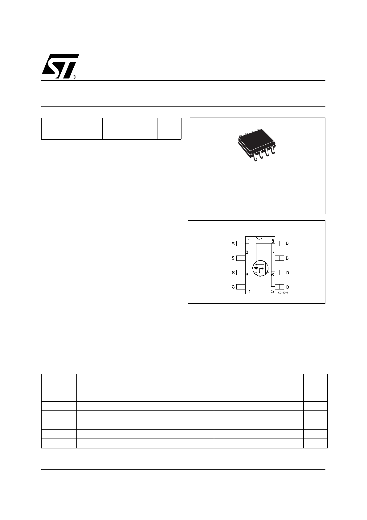
SO-8
INTERNAL SCHEMATIC DIAGRAM
ABSOLUTE MAXIMUM RATINGS
Symbol Parameter Value Unit
V
DS
V
DGR
V
GS
I
D
I
D
I
DM
P
TOT
(●) Pulse width limited by safe operating area
December 2002
Drain-source Voltage (VGS=0)
Drain-gate Voltage (RGS=20kΩ)
Gate- source Voltage ±20 V
Drain Current (continuous) at TC= 25°C
Drain Current (continuous) at TC= 100°C
Drain Current (pulsed) 28 A
Total Dissipation at TC= 25°C
Note: For the P-CHANNEL MOSFET actual polarity of voltages and
30 V
30 V
7A
4.4 A
2.5 W
current has to be reversed
1/6
Page 2
STS7PF30L
THERMAL DATA
Rthj-amb(#) Thermal Re sistance Junction-ambient Max 50 °C/W
Tj Maxim um Lead Temperature For Soldering Purpose Typ 150 °C
T
stg
(#) When mounted on 1 inch2FR4 Board, 2 oz of Cu and t ≤ 10s
ELECTRICAL CHARACTERISTICS (TJ= 25 °C UNLESS OTHERRWISE SPECIFIED)
OFF
Symbol Parameter Test Conditions Min. Typ. Max. Unit
V
(BR)DSS
I
DSS
I
GSS
ON (1)
Symbol Parameter Test Conditions Min. Typ. Max. Unit
V
GS(th)
R
DS(on)
Storage Temperature –55 to 150 °C
Drain-source
ID= 250 µA, VGS= 0 30 V
Breakdown Voltage
Zero Gate Voltage
Drain Current (V
GS
=0)
Gate-body Lea kage
Current (V
DS
=0)
Gate Threshold Voltage
Static Drain-source On
Resistance
V
= Max Rating
DS
V
= Max Rating , TC= 125 °C
DS
V
= ± 20V ±100 nA
GS
V
DS=VGS,ID
VGS=10V,ID= 3.5A
= 4.5V, ID= 3.5A
V
GS
= 250µA
1 1.6 2.5 V
0.011 0.016 0.021 Ω
0.016 0.022 0.028 Ω
1µA
10 µA
DYNAMIC
Symbol Parameter Test Conditions Min. Typ. Max. Unit
g
fs
C
iss
C
oss
C
rss
Forward Transconductanc e VDS=10V,ID= 3.5A 16 S
V
Input Capacitance
=25V,f=1MHz,VGS=0
DS
2600 pF
Output Capacitance 523 pF
Reverse Transfer
174 pF
Capacitance
2/6
Page 3

STS7PF30L
ELECTRICAL CHARACTERISTICS (CONTINUED)
SWITCHING ON(2)
Symbol Parameter Test Conditions Min. Typ. Max. Unit
V
t
d(on)
Q
Q
Q
t
r
g
gs
gd
Turn-on Delay Time
Rise Time 54 ns
Total Gate Charge
Gate-Source Charge
Gate-Drain Charge
SWITCHING OFF(2)
Symbol Parameter Test Conditions Min. Typ. Max. Unit
t
d(off)
t
f
Turn-off-Delay Time
Fall Time
SOURCE DRAIN DIODE (2)
Symbol Parameter Test Conditions Min. Typ. Max. Unit
I
SD
I
SDM
VSD(2)
t
rr
Q
rr
I
RRM
Note: 1. Pulsed: Pulse duration = 300 µs, duty cycle 1.5 %.
2. Pulse w idth limited by safe operating area.
Source-drain Current 7 A
(1)
Source-drain Current (pulsed) 28 A
Forward On Voltage
Reverse Recovery Time
Reverse Recovery Charge
Reverse Recovery Current
=15V,ID= 3.5A
DD
= 4.7Ω VGS=4.5V
R
G
(Resistive Load, Figure 3)
=15V,ID=7A,
V
DD
V
= 4.5V
GS
VDD=15 V,ID= 3.5 A,
RG=4.7Ω, VGS= 4.5 V
(Resistive Load, Figure 3)
ISD= 7 A, VGS=0
= 7A, di/dt = 100A/µs,
I
SD
VDD=24V,Tj= 150°C
(see test circuit, Figure 5)
68 ns
28
38
8.8
12
65
23
1.2 V
40
46
2.3
nC
nC
nC
ns
ns
ns
nC
A
3/6
Page 4

STS7PF30L
Fig. 2: Unclam ped Inductive WaveformFig. 1: Unclamped Inducti ve Load T es t Circuit
Fig. 3: Switching Times Test Circuit For
Resistive Load
Fig. 5: Test Circuit For Inductive Load Switching
And Diode Recovery Times
Fig. 4: Gate Charge test Circuit
4/6
Page 5

0016023
SO-8 MECHANICAL DATA
STS7PF30L
DIM.
MIN. TYP. MAX. MIN. TYP. MAX.
A1.750.068
a1 0.1 0.25 0.003 0.009
a2 1.65 0.064
a3 0.65 0.85 0.025 0.033
b 0.35 0.48 0.013 0.018
b1 0.19 0.25 0.007 0.010
C 0.25 0.5 0.010 0.019
c1 45 (typ.)
D 4.8 5.0 0.188 0.196
E 5.8 6.2 0.228 0.244
e1.27 0.050
e3 3.81 0.150
F 3.8 4.0 0.14 0.157
L 0.4 1.27 0.015 0.050
M0.60.023
S 8 (max.)
mm inch
5/6
Page 6

STS7PF30L
Information furnished is believed to be accurate and reliable. However, STMicroelectronics assumes no responsibility for the
consequences of use of su ch in formation nor for any in fringement of patents or other rights of third parties w hich may result from
its use. No license is granted by implication or otherwise under any patent or patent rights of STMicroelectronics. Specifications
mentioned in this publication are subject to change without notice. This publication supersedes and replaces all information
previously suppli ed. STMi croelect ronics pr oducts are not author ized for use as cr itical component s in li fe suppo rt devi ces or
systems without express written approval of STMicroelectronics.
Australia - Brazil - Canada - China - Finland - France - Germany - Hong Kong - India - Israel - Italy - Japan - Malaysia - Malta - Morocco
© The ST logo is a registered trademark of STMicroelectronics
© 2002 STMicroelectronics - Printed in Italy - All Rights Reserved
Singapore - Spain - Sweden - Switzerland - United Kingdom - United States.
STMicroelectronics GROUP OF COMPANIES
© http://www.st.com
6/6
 Loading...