

Page 1
®
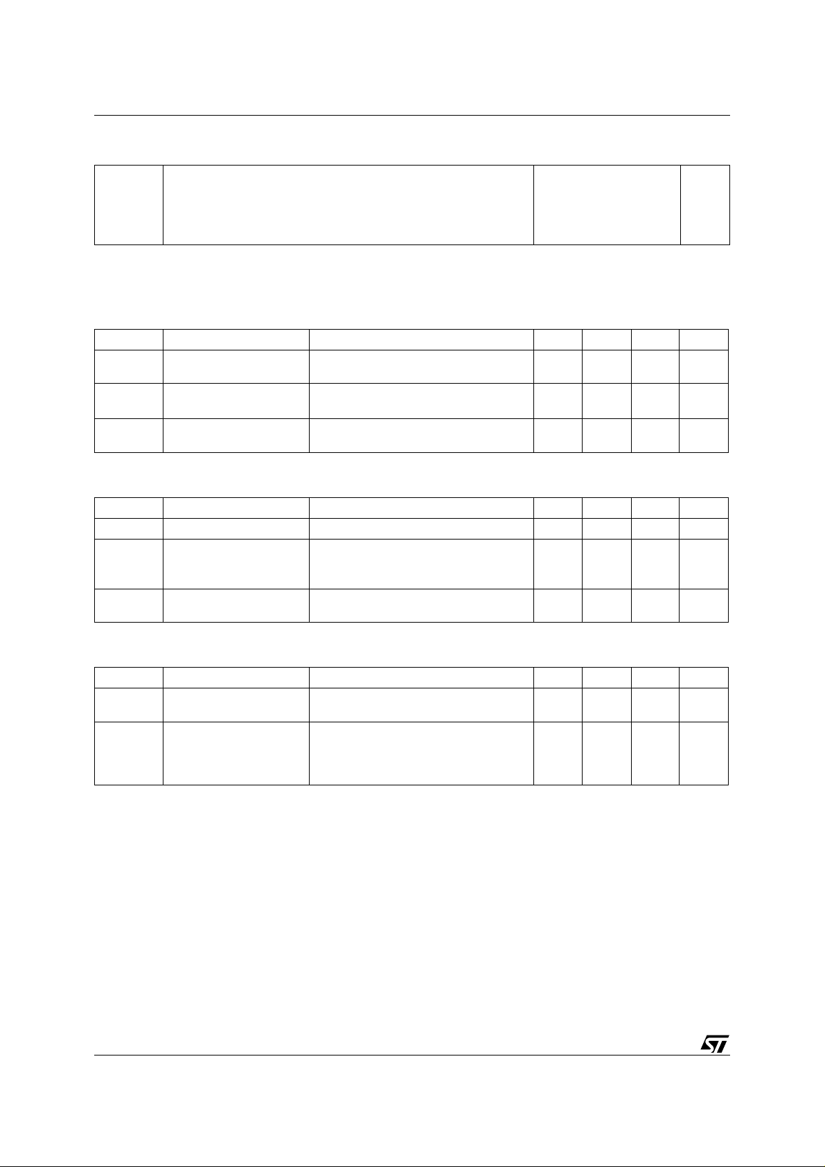
N - CHANNEL 30V - 0.021Ω - 7A SO-8
TYPE V
STS7NF30L 30 V < 0.025 Ω 7 A
■
TYPICAL R
■
STANDARD OUTLINE FOR EASY
DS(on)
DSS
= 0.021
AUTOMATED SURF ACE MOUNT ASSEMBLY
■
LOW THRESHOLD DRIVE
DESCRIPTION
This Power MOSFET is the second generation of
STMicroelectronics unique " Single Feature
Size " strip-based process. The resulting
transistor shows extremely high packing density
for low on-resistance, rugged avalanche
characteristics and less critical alignment steps
therefore a remarkable manufacturing
reproducibility.
Ω
R
DS(on)
I
D
STS7NF30L
STripFET POWER MOSFET
PRELIMINARY DATA
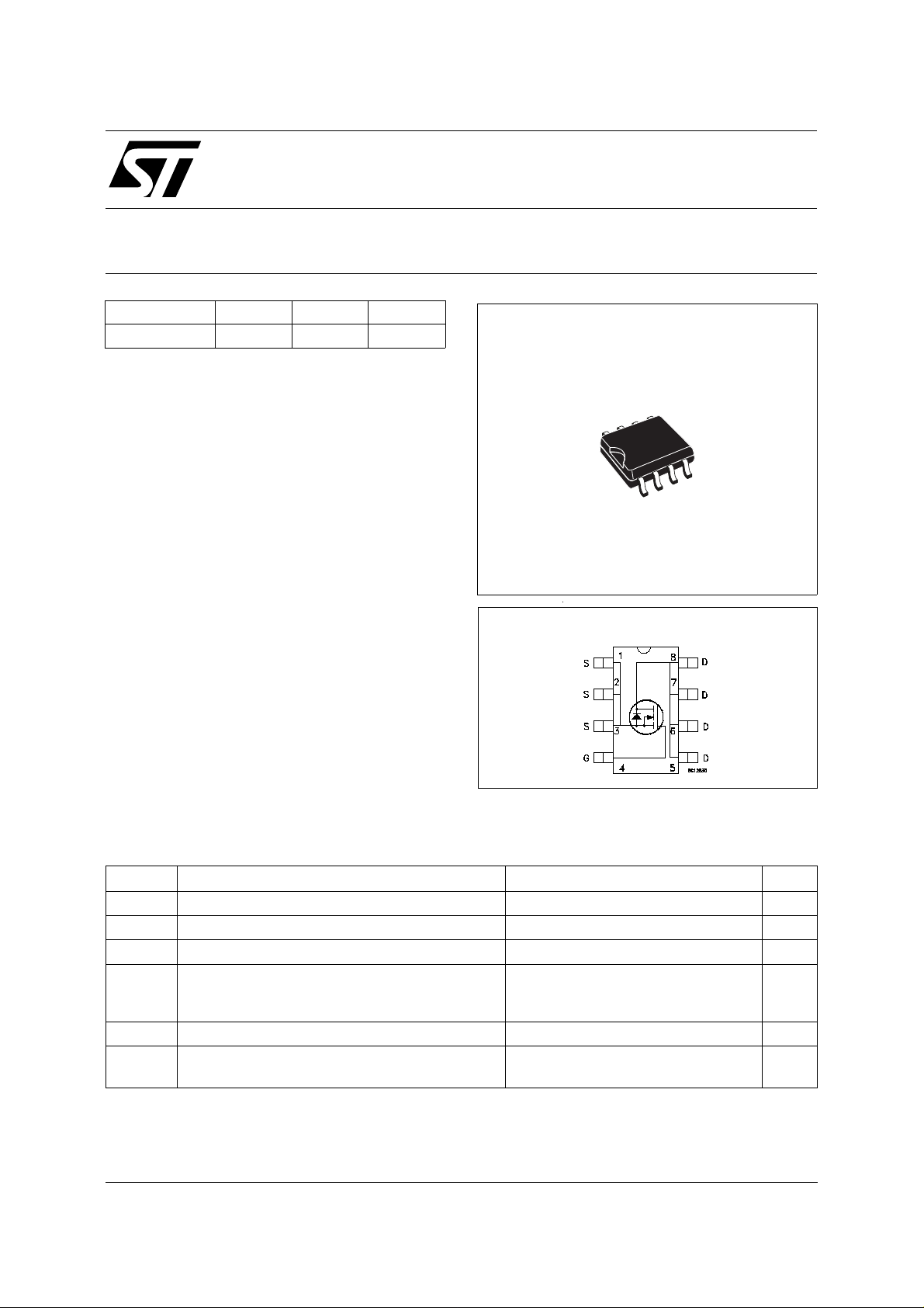
SO-8
APPLICATIONS
■
DC MOTOR DRIVE
■
DC-DC CONVERTERS
■
BATTERY MANAGM ENT IN NOMADI C
INTERNAL SCHEMATIC DIAGRAM
EQUIPMENT
■
POWER MANAGEMENT IN
PORTABLE/DESKTOP PC
s
ABSOLUTE MAXIMUM RATINGS
Symbol Parameter Value Unit
I
V
V
V
DM
P
Drain-source Voltage (VGS = 0) 30 V
DS
Drain- gate Voltage (RGS = 20 kΩ)
DGR
Gate-source Voltage ± 20 V
GS
I
Drain Current (continuous) at Tc = 25 oC
D
Drain Current (continuous) at T
(•) Drain Current (pulsed) 42 A
Total Dissipation at Tc = 25 oC 2.5 W
tot
= 100 oC
c
30 V
7
4.4
A
A
(•) Pulse width limited by safe operating area
May 1999
1/5
Page 2
STS7NF30L
THERMAL DATA
R
thj-amb
T
T
(*)Thermal Resistance Junction-ambient
Maximum Operating Junction Temperature
j
Storage Temperature
stg
50
150
-55 to 150
o
C/W
o
o
C
C
(*)
Mounted on FR-4 board ( (t
ELECTRICAL CHARACTERISTICS
≤ 10sec)
(T
case
= 25 oC unless otherwise specified)
OFF
Symbol Parameter Test Conditions Min. Typ. Max. Unit
V
(BR)DSS
Drain-source
I
= 250 µA V
D
GS
= 0
30 V
Breakdown Voltage
I
I
ON (∗
DSS
GSS
Zero Gate Voltage
Drain Current (V
Gate-body Leakage
Current (V
)
DS
= 0)
GS
= 0)
= Max Rating
V
DS
V
= Max Rating Tc = 125 oC
DS
V
= ± 20 V
GS
1
10
± 100 nA
Symbol Parameter Test Conditions Min. Typ. Max. Unit
V
R
DS(on)
I
D(on)
GS(th)
Gate Threshold Voltage
Static Drain-source On
Resistance
V
= VGS ID = 250 µA
DS
VGS = 10 V ID = 3.5 A
V
= 4.5 V ID = 3.5 A
GS
On State Drain Current VDS > I
V
= 10 V
GS
D(on)
x R
DS(on)max
1 1.6 2.5 V
0.021
0.025
20 A
0.025
0.032ΩΩ
DYNAMIC
µA
µA
Symbol Parameter Test Conditions Min. Typ. Max. Unit
g
(∗) Forward
fs
VDS > I
D(on)
x R
DS(on)max
ID = 3.5 A 10 S
Transconductance
C
C
C
Input Capacitance
iss
Output Capacitance
oss
Reverse Transfer
rss
V
= 25 V f = 1 MHz V
DS
= 0 V 1250
GS
230
50
Capacitance
2/5
pF
pF
pF
Page 3

STS7NF30L
ELECTRICAL CHARACTERISTICS (continued)
SWITCHING ON
Symbol Parameter Test Conditions Min. Typ. Max. Unit
t
d(on)
Turn-on Delay Time
Rise Time
t
r
V
= 15 V ID = 3 A
DD
= 4.7 Ω VGS = 5 V
R
G
(Resistive Load, see fig. 3)
Q
Q
Q
Total Gate Charge
g
Gate-Source Charge
gs
Gate-Drain Charge
gd
V
= 24 V ID = 7 A V
DD
= 4.5 V 17
GS
SWITCHING OFF
Symbol Parameter Test Conditions Min. Typ. Max. Unit
t
d(off)
Turn-off Delay Time
Fall Time
t
f
V
= 15 V ID = 3 A
DD
= 4.7 Ω VGS = 5 V
R
G
(Resistive Load, see fig. 3)
t
r(Voff)
t
t
Off-voltage Rise Time
Fall Time
f
Cross-over Time
c
V
= 24 V ID = 7 A
clamp
= 4.7 Ω VGS = 5 V
R
G
(Inductive Load, see fig. 5)
SOURCE DRAIN DIODE
22
30
23 nC
4
6
55
10
10
18
30
ns
ns
nC
nC
ns
ns
ns
ns
ns
Symbol Parameter Test Conditions Min. Typ. Max. Unit
2
8
I
SDM
I
SD
Source-drain Current
(•)
Source-drain Current
(pulsed)
V
(∗) Forward On Voltage ISD = 7 A VGS = 0 1.2 V
SD
t
Q
Reverse Recovery
rr
Time
Reverse Recovery
rr
I
= 7 A di/dt = 100 A/µs
SD
V
= 20 V Tj = 150 oC
DD
(see test circuit, fig. 5)
30
30
Charge
I
RRM
Reverse Recovery
2
Current
(∗) Pulsed: Pulse duration = 300 µs, duty cycle 1.5 %
(•) Pulse width limited by safe operating area
A
A
ns
nC
A
3/5
Page 4

STS7NF30L
SO-8 MECHANICAL DATA
DIM.
MIN. TYP. MAX. MIN. TYP. MAX.
A1.750.068
a1 0.1 0.25 0.003 0.009
a2 1.65 0.064
a3 0.65 0.85 0.025 0.033
b 0.35 0.48 0.013 0.018
b1 0.19 0.25 0.007 0.010
C 0.25 0.5 0.010 0.019
c1 45 (typ.)
D 4.8 5.0 0.188 0.196
E 5.8 6.2 0.228 0.244
e1.27 0.050
e3 3.81 0.150
F 3.8 4.0 0.14 0.157
L 0.4 1.27 0.015 0.050
M0.60.023
S 8 (max.)
mm inch
4/5
0016023
Page 5

STS7NF30L
Information f urnished i s believed t o be accurate an d reliabl e. How ever, STMicroelect ronics assu mes no responsib ility fo r the consequen ces
of use of such information nor for any infringement of patents or other rights of third parties which may result from its use. No license is
granted by implication or otherwise under any patent or patent rights of STMicroelectronics. Specification mentioned in this publication are
subject to chan ge w ithout notice. This publicatio n su persedes a nd r eplaces al l inf ormati on previ ously suppl ied. STMicroelect ron ics produ cts
are not auth ori zed f or use as critical component s in life support devices or systems without exp ress writ te n approval of STMicroelectronics.
The ST logo is a trademark of STMicroelectronics
© 1999 STMicroelect ronics – Printed in Italy – Al l Rights Reserved
STMicroele ct ronics GROUP OF COMPANIES
Australia - Brazil - Canada - China - France - Germany - Italy - Japan - Korea - Malaysia - Malta - Mexico - Morocco - The Netherlands -
Singapore - Spain - Sweden - Switzer land - Taiwan - Thailand - Un it ed Kingdom - U.S.A.
http://www.st.com
.
5/5
 Loading...