

Page 1
®
N - CHANNEL 60V - 0.045Ω - 5A SO-8
TYPE V
STS5NF60L 60 V < 0.055 Ω 5 A
■
TYPICAL R
■
STANDARD OUTLINE FOR EASY
DS(on)
DSS
= 0.045
AUTOMATED SUR F ACE MOUNT ASSEMBLY
■
LOW THRESHOLD DRIVE
DESCRIPTION
This Power MOSFET is the second generation of
STMicroelectronics unique " Single Feature
Size " strip-based process. The resulting
transistor shows extremely high packing density
for low on-resistance, rugged avalanche
characteristics and less critical alignment steps
therefore a remarkable manufacturing
reproducibility.
APPLICATIONS
■
DC MOTOR DRIVE
■
DC-DC CONVERTERS
■
BATTERY MANAGM ENT IN NOMADI C
EQUIPMENT
■
POWER MANAGEMENT IN
PORTABLE/DESKTOP PC
Ω
R
DS(on)
s
I
D
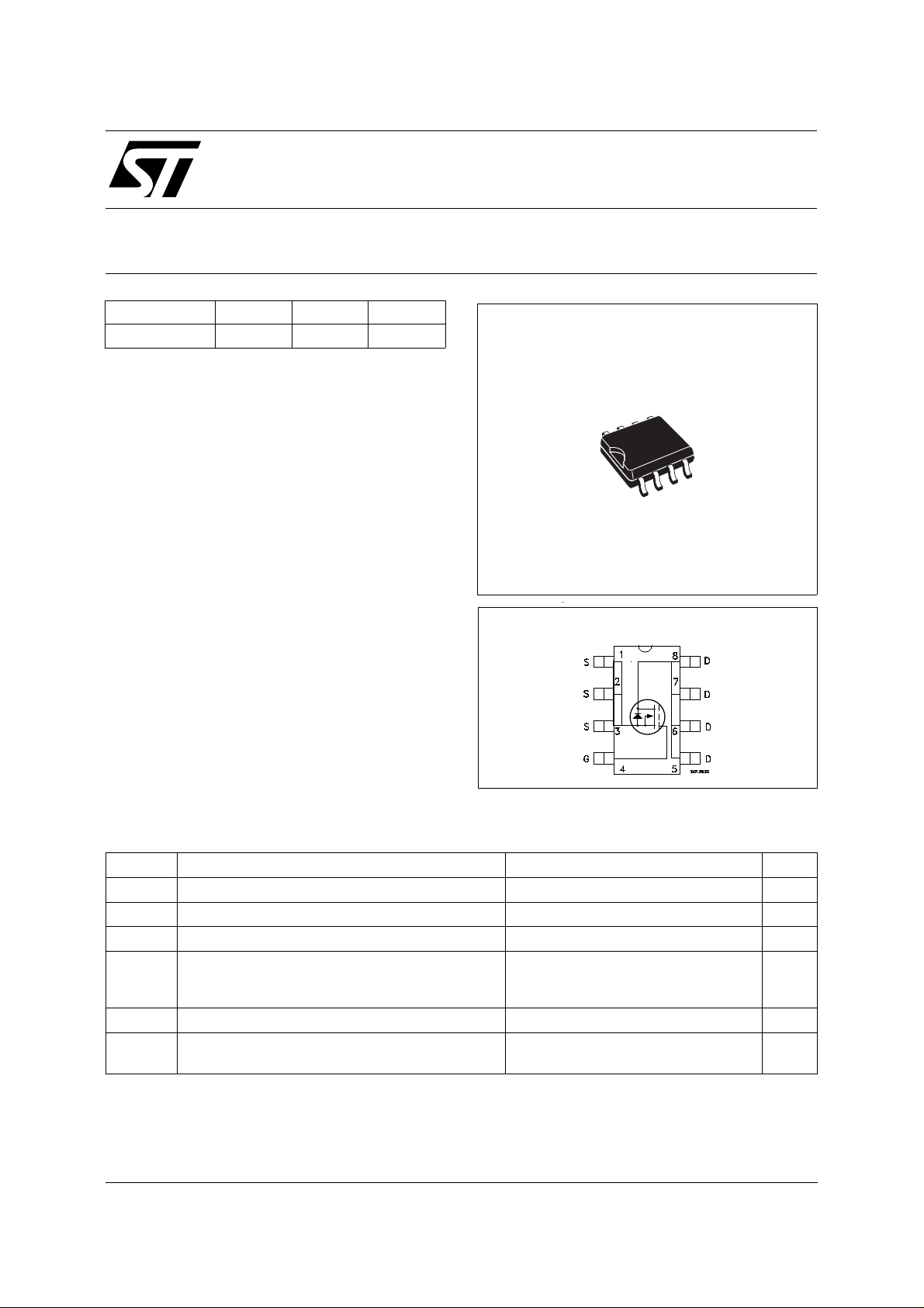
STS5NF60L
STripFET POWER MOSFET
PRELIMINARY DATA
SO-8
INTERNAL SCHEMATIC DIAGRAM
ABSOLUTE MAXIMUM RATINGS
Symbol Parameter Value Unit
V
V
V
I
DM
P
(•) Pulse width limited by safe operating area
December 1998
Drain-source Voltage (VGS = 0) 60 V
DS
Drain- gate Voltage (RGS = 20 kΩ)
DGR
Gate-source Voltage ± 20 V
GS
I
Drain Current (continuous) at Tc = 25 oC
D
Drain Current (continuous) at T
(•) Drain Current (pulsed) 20 A
Total Dissipation at Tc = 25 oC 2.5 W
tot
= 100 oC
c
60 V
5
3
A
A
1/5
Page 2
STS5NF60L
THERMAL DATA
R
thj-amb
T
T
(*)Thermal Resistance Junction-ambient
Maximum Operating Junction Temperature
j
Storage Temperature
stg
50
150
-55 to 150
o
C/W
o
o
C
C
(*)
Mounted on FR-4 board (t
ELECTRICAL CHARACTERISTICS
≤ 10sec)
(T
= 25 oC unless otherwise specified)
case
OFF
Symbol Parameter Test Conditions Min. Typ. Max. Unit
V
(BR)DSS
Drain-source
I
= 250 µA V
D
GS
= 0
60 V
Breakdown Voltage
I
I
ON (∗
DSS
GSS
Zero Gate Voltage
Drain Current (V
Gate-body Leakage
Current (V
)
DS
= 0)
GS
= 0)
= Max Rating
V
DS
V
= Max Rating Tc = 125 oC
DS
= ± 20 V
V
GS
1
10
± 100 nA
Symbol Parameter Test Conditions Min. Typ. Max. Unit
V
R
DS(on)
I
D(on)
GS(th)
Gate Threshold Voltage
Static Drain-source On
Resistance
= VGS ID = 250 µA
V
DS
VGS = 10 V ID = 2.5 A
V
= 4.5 V ID = 2.5 A
GS
On State Drain Current VDS > I
V
= 10 V
GS
D(on)
x R
DS(on)max
1 1.7 2.5 V
0.045
0.05
0.055
0.065ΩΩ
5A
DYNAMIC
µA
µA
Symbol Parameter Test Conditions Min. Typ. Max. Unit
g
(∗) Forward
fs
VDS > I
D(on)
x R
DS(on)max
ID = 2.5 A 7 S
Transconductance
C
C
C
Input Capacitance
iss
Output Capacitance
oss
Reverse Transfer
rss
V
= 25 V f = 1 MHz V
DS
= 0 V 1250
GS
130
26
Capacitance
2/5
pF
pF
pF
Page 3

STS5NF60L
ELECTRICAL CHARACTERISTICS (continued)
SWITCHING ON
Symbol Parameter Test Conditions Min. Typ. Max. Unit
t
d(on)
t
r
Turn-on Time
Rise Time
V
= 15 V ID = 2.5 A
DD
= 4.7 Ω VGS = 4.5 V
R
G
TBD TBD ns
ns
Q
Q
Q
Total Gate Charge
g
Gate-Source Charge
gs
Gate-Drain Charge
gd
V
= 48 V ID = 5 A V
DD
= 4.5 V 25 nC
GS
SWITCHING OFF
Symbol Parameter Test Conditions Min. Typ. Max. Unit
t
r(Voff)
t
t
Off-voltage Rise Time
Fall Time
f
Cross-over Time
c
V
= 48 V ID = 5 A
DD
= 4.7 Ω VGS = 4.5 V
R
G
TBD TBD ns
SOURCE DRAIN DIODE
Symbol Parameter Test Conditions Min. Typ. Max. Unit
5
20
I
SDM
I
SD
Source-drain Current
(•)
Source-drain Current
(pulsed)
V
(∗) Forward On Voltage ISD = 5 A VGS = 0 1.2 V
SD
t
Q
Reverse Recovery
rr
Time
Reverse Recovery
rr
I
= 5 A di/dt = 100 A/µs
SD
V
= 20 V Tj = 150 oC
r
TBD ns
Charge
I
RRM
Reverse Recovery
Current
(∗) Pulsed: Pulse duration = 300 µs, duty cycle 1.5 %
(•) Pulse width limited by safe operating area
nC
nC
ns
ns
A
A
nC
A
3/5
Page 4

STS5NF60L
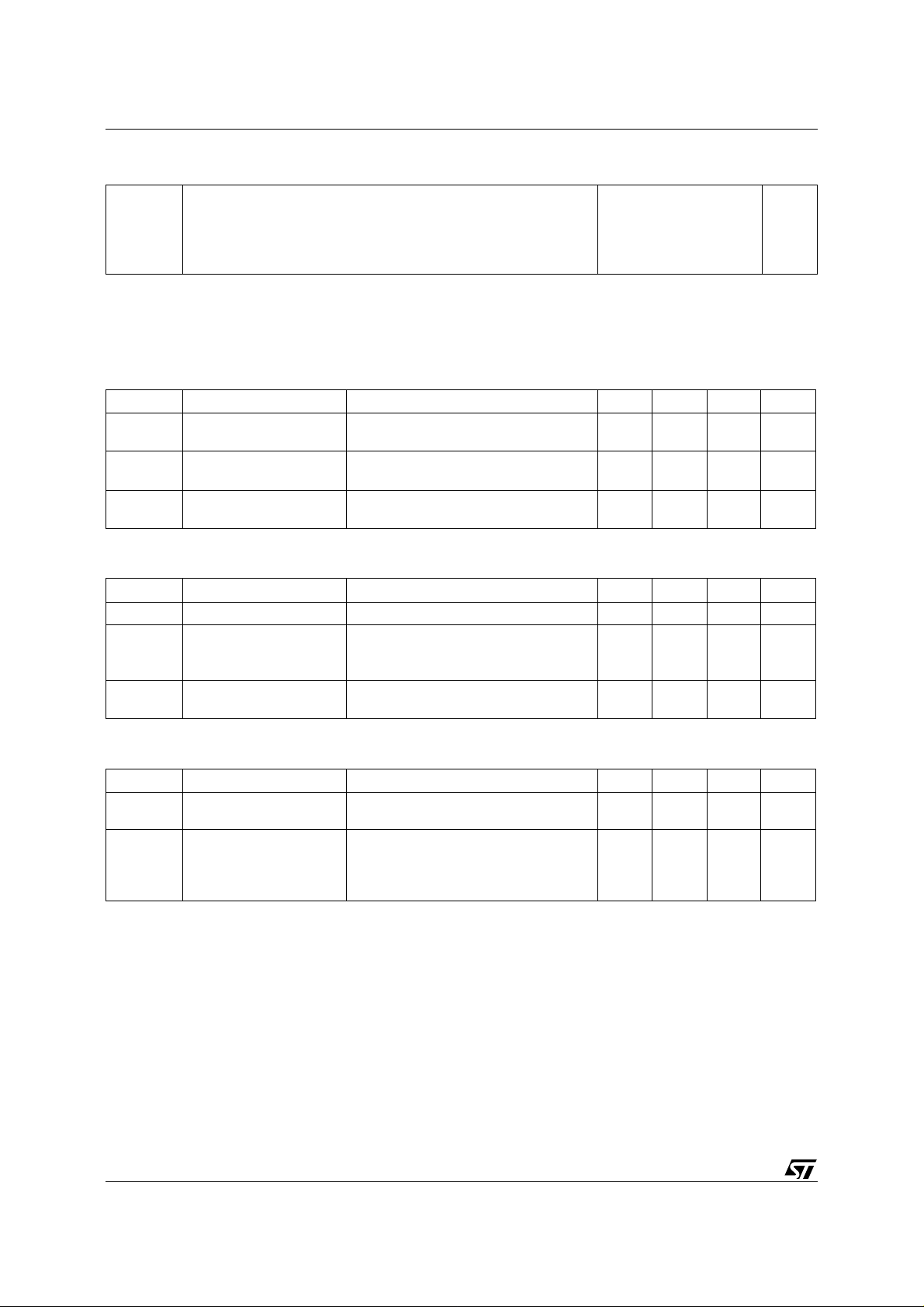
SO-8 MECHANICAL DATA
DIM.
MIN. TYP. MAX. MIN. TYP. MAX.
A1.750.068
a1 0.1 0.25 0.003 0.009
a2 1.65 0.064
a3 0.65 0.85 0.025 0.033
b 0.35 0.48 0.013 0.018
b1 0.19 0.25 0.007 0.010
C 0.25 0.5 0.010 0.019
c1 45 (typ.)
D 4.8 5.0 0.188 0.196
E 5.8 6.2 0.228 0.244
e1.27 0.050
e3 3.81 0.150
F 3.8 4.0 0.14 0.157
L 0.4 1.27 0.015 0.050
M0.60.023
S 8 (max.)
mm inch
4/5
0016023
Page 5

STS5NF60L
Information furnished is believed to be accurate and reliable. However, STMicroelectronics assumes no responsibility for the consequences
of use of such inform ation nor for any in fringe ment o f patents or other rig hts of third par ties wh ich may result from its u se. N o li cen se is
granted by implication or otherwise under any patent or patent rights of STMicroelectronics. Specification mentioned in this publication are
subject to change without notice. This publication supersedes and replaces all information previously supplied. STMicroelectronics products
are not authorized f or use as critical components in life support devices or systems without express written approval of STMicroelectronics.
The ST logo is a trademark of STMicroelectronics
© 1998 STMicroelectro nics – Printed in Italy – All Rights Reserved
STMicroelectronics GROUP OF COMPANIES
Australia - Brazil - Canada - China - France - Germany - Italy - Japan - Korea - Malaysia - Malta - Mexico - Morocco - The Netherlands -
Singapore - Spain - Sweden - Switzerland - Taiwan - Thailand - United Kingdom - U.S.A.
http://www.st.com
.
5/5
 Loading...