

Page 1
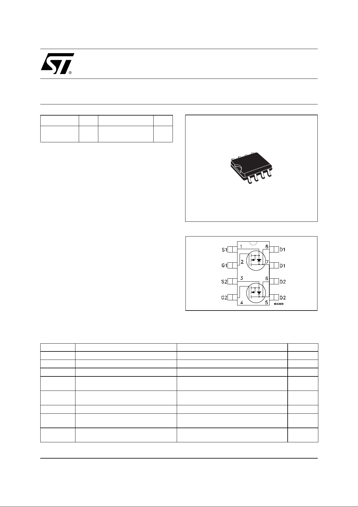
STS5DNF20V
N-CHANNEL 20V - 0.030 Ω - 5A SO-8
2.7V-DRIVE STripFET™ II POWER MOSFET
TYPE
V
DSS
STS5DNF20V 20 V
■ TYPICAL R
■ TYPICAL R
■ ULTRA LOW THRESHOLD
(on) = 0.030 Ω @ 4.5 V
DS
(on) = 0.037 Ω @ 2.7 V
DS
R
DS(on)
< 0.040 Ω ( @ 4.5 V )
< 0.045 Ω ( @ 2.7 V )
I
D
5 A
GATE DRIVE (2.7 V)
■ STANDARD OUTLI NE FO R EASY
AUTOMATED SURFACE MOUNT ASSEMBLY
DESCRIPTION
This Power MOSFET is the latest dev elo pment of
STMicroelectronis unique "Single Feature Size™"
strip-based process. The resulting transistor
shows extremely high packing density for low onresistance, rugged avalanche characteristics and
less critical alignment steps therefore a remarkable manufacturing reproducibility.
APPLICATIONS
■ DC MOTOR DRIVE
■ DC-DC CONVERTERS
■ BATTERY MANAGEMENT IN NOMADIC
EQUIPMENT
■ POWER MANAGEMENT IN
PORTABLE/DESKTOP PCs
SO-8
INTERNAL SCHEMATIC DIAGRAM
ABSOLUTE MAXIMUM RATINGS
Symbol Parameter Value Unit
V
DS
V
DGR
V
GS
I
D
I
D
I
(
DM
P
tot
P
tot
(
Pulse widt h l i m i ted by safe operating area.
•)
.
Drain-source Voltage (VGS = 0)
Drain-gate Voltage (RGS = 20 kΩ)
20 V
20 V
Gate- source Voltage ± 12 V
Drain Current (continuous) at TC = 25°C
Single Operation
Drain Current (continuous) at TC = 100°C
Single Operation
•)
Drain Current (pulsed) 20 A
Total Dissipation at TC = 25°C
Dual Operation
Total Dissipation at TC = 25°C
Single Operation
5A
3A
1.6 W
2W
1/8August 2002
Page 2
STS5DNF20V
THERMA L D ATA
Rthj-amb
T
T
stg
Thermal Resistance Junction-ambient Single Operation
Thermal Resistance Junction-ambient Dual Operation
Max. Operating Junction Temperature
j
Storage Temperature
Max
Max
62.5
78
-55 to 150
-55 to 150
°C/W
°C/W
°C
°C
ELECTRICAL CHARACTERISTICS (T
= 25 °C unless otherwise specified)
case
OFF
Symbol Parameter Test Conditions Min. Typ. Max. Unit
I
V
(BR)DSS
Drain-source
= 250 µA, VGS = 0
D
20
Breakdown Voltage
V
= Max Rating
DS
V
= Max Rating TC = 125°C
DS
= ± 12V
V
GS
1
10
±100 nA
ON
(*)
I
DSS
I
GSS
Zero Gate Voltage
Drain Current (V
GS
Gate-body Leakage
Current (V
DS
= 0)
= 0)
Symbol Parameter Test Conditions Min. Typ. Max. Unit
V
V
GS(th)
R
DS(on)
Gate Threshold Voltage
Static Drain-source On
Resistance
= VGS ID = 250 µA
DS
= 4.5 V ID = 2.5 A
V
GS
V
= 2.7 V ID = 2.5 A
GS
0.6 V
0.030
0.037
0.040
0.045
DYNAMIC
Symbol Parameter Test Conditions Min. Typ. Max. Unit
(*)
g
fs
C
iss
C
oss
C
rss
Forward Transconductance
Input Capacitance
Output Capacitance
Reverse Transfer
Capacitance
V
=15 V ID= 2.5 A
DS
= 15V f = 1 MHz, VGS = 0
V
DS
10 S
460
200
50
V
µA
µA
Ω
Ω
pF
pF
pF
2/8
Page 3
STS5DNF20V
ELECTRICAL CHARACTERISTICS (continued)
SWITCHING ON
Symbol Parameter Test Conditions Min. Typ. Max. Unit
= 10 V ID = 2.5 A
t
d(on)
Turn-on Delay Time
t
r
Rise Time
V
DD
R
= 4.7 Ω VGS = 4.5 V
G
(Resistive Load, Figure 1)
Q
g
Q
gs
Q
gd
Total Gate Charge
Gate-Source Charge
Gate-Drain Charge
= 16V ID= 5A VGS=4.5V
V
DD
(see test circuit, Figure 2)
SWITCHING OFF
Symbol Parameter Test Conditions Min. Typ. Max. Unit
= 10 V ID = 2.5 A
t
d(off)
Turn-off Delay Time
t
f
Fall Time
V
DD
R
= 4.7Ω, V
G
GS
= 4.5 V
(Resistive Load, Figure 1)
SOURCE DRAIN DIODE
Symbol Parameter Test Conditions Min. Typ. Max. Unit
I
SD
I
SDM
V
SD
t
rr
Q
rr
I
RRM
(*)
Pulsed: P ul se duration = 300 µs, duty cycle 1.5 %.
(
•)Pulse width limited by s afe operating area.
Source-drain Current
(•)
Source-drain Current (pulsed)
(*)
Forward On Voltage
Reverse Recovery Time
Reverse Recovery Charge
Reverse Recovery Current
I
= 5 A VGS = 0
SD
= 5 A di/dt = 100A/µs
I
SD
V
= 10 V Tj = 150°C
DD
(see test circuit, Figure 3)
7
33
8.5
1.8
2.4
27
10
26
13
1
11.5 nC
5
20
1.2 V
ns
ns
nC
nC
ns
ns
A
A
ns
nC
A
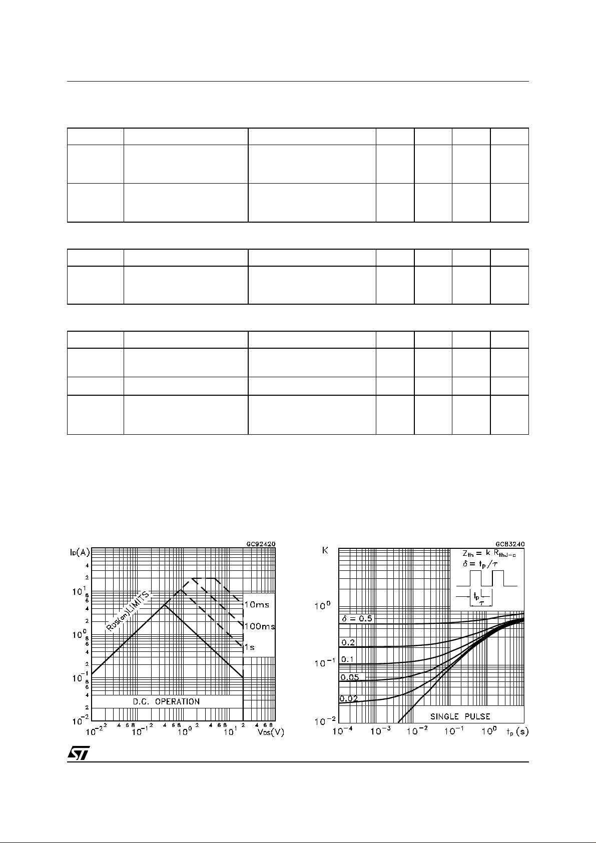
Safe Operating Area
Thermal Impedance
3/8
Page 4

STS5DNF20V
Output Characteristics Transfer Characteristics
Transconductance Static Drain-source On Resistance
Gate Charge vs Gate-source Voltage Capacitance Variations
4/8
Page 5

STS5DNF20V
Normalized Gate Threshold Voltage vs Temperature Normalized on Resistance vs Temperature
Source-drain Diode Forward Characteristics .
. .
5/8
Page 6

STS5DNF20V
Fig. 1: Switching Times Test Circuits For Resistive
Load
Fig. 3: Test Circuit For Diode Recovery Behaviour
Fig. 2: Gate Charge test Circuit
6/8
Page 7

SO-8 MECHANICAL DATA
STS5DNF20V
DIM.
MIN. TYP. MAX. MIN. TYP. MAX.
A1.750.068
a1 0.1 0.25 0.003 0.009
a2 1.65 0.064
a3 0.65 0.85 0.025 0.033
b 0.35 0.48 0.013 0.018
b1 0.19 0.25 0.007 0.010
C 0.25 0.5 0.010 0.019
c1 45 (typ.)
D 4.8 5.0 0.188 0.196
E 5.8 6.2 0.228 0.244
e1.27 0.050
e3 3.81 0.150
F 3.8 4.0 0.14 0.157
L 0.4 1.27 0.015 0.050
M0.60.023
S 8 (max.)
mm inch
0016023
7/8
Page 8

STS5DNF20V
Information furnished is believed to be accurate and reliable. However, STM ic roelectronics assu m es no responsibility for the co nsequences
of use of such information nor for any infringement of patents or other rights of third parties which may result from its use. No license is granted
by implic ation or o th erwise under any patent or patent rights of STM i croelectr onics. Sp ecifications mentioned in th i s publicati on are subject
to change without notice. This publication supersedes and replaces all information previously supplied. STMicroelectronics products are not
authorized for use as cri tical comp onents in lif e support dev i ces or systems wi thout exp ress written approval of STMicro el ectronics.
The ST log o i s registered trademark of STMic roelectronics
2001 STMi croelectronics - All Ri ghts Reserved
All other names are the property of their respective ow ners.
Australi a - Brazil - Ch i na - Finland - F rance - Germ any - Hong Kong - India - Ita l y - Japan - Malaysia - Malt a - Morocco -
Singapor e - Spain - Sweden - Switz erl and - United Kingdom - U.S.A.
STMicroelect ro n ics GRO UP OF COMPANI ES
http://www.st.com
8/8
 Loading...