

Page 1
STS4NF100
N-CHANNEL 100V - 0.065 Ω - 4A SO-8
STripFET™ II POWER MOSFET
TYPE
V
DSS
STS4NF100 100 V <0.070
■ TYPICAL R
■ EXCEPTIONA L dv/d t CAPABILITY
■ 100 % AVALANCHE TESTED
■ APPLICATION ORIENTED
(on) = 0.065 Ω
DS
R
DS(on)
I
D
4 A
Ω
CHARACTERIZATION
DESCRIPTION
This MOSFET series realized with STMicroelectronics
unique STripFET process has specifically been designed
to minimize input capacitance and gate charge. It is
therefore suitable as primary switch in advanced highefficiency, high-frequency isolate d DC-DC c onverters for
Telecom and Computer a pplications. It is also intended
for any applications with low gate drive requirements.
APPLICATIONS
■ HIGH-EFFICIENCY DC-DC CONVERTERS
■ UPS AND MOTOR CONTROL
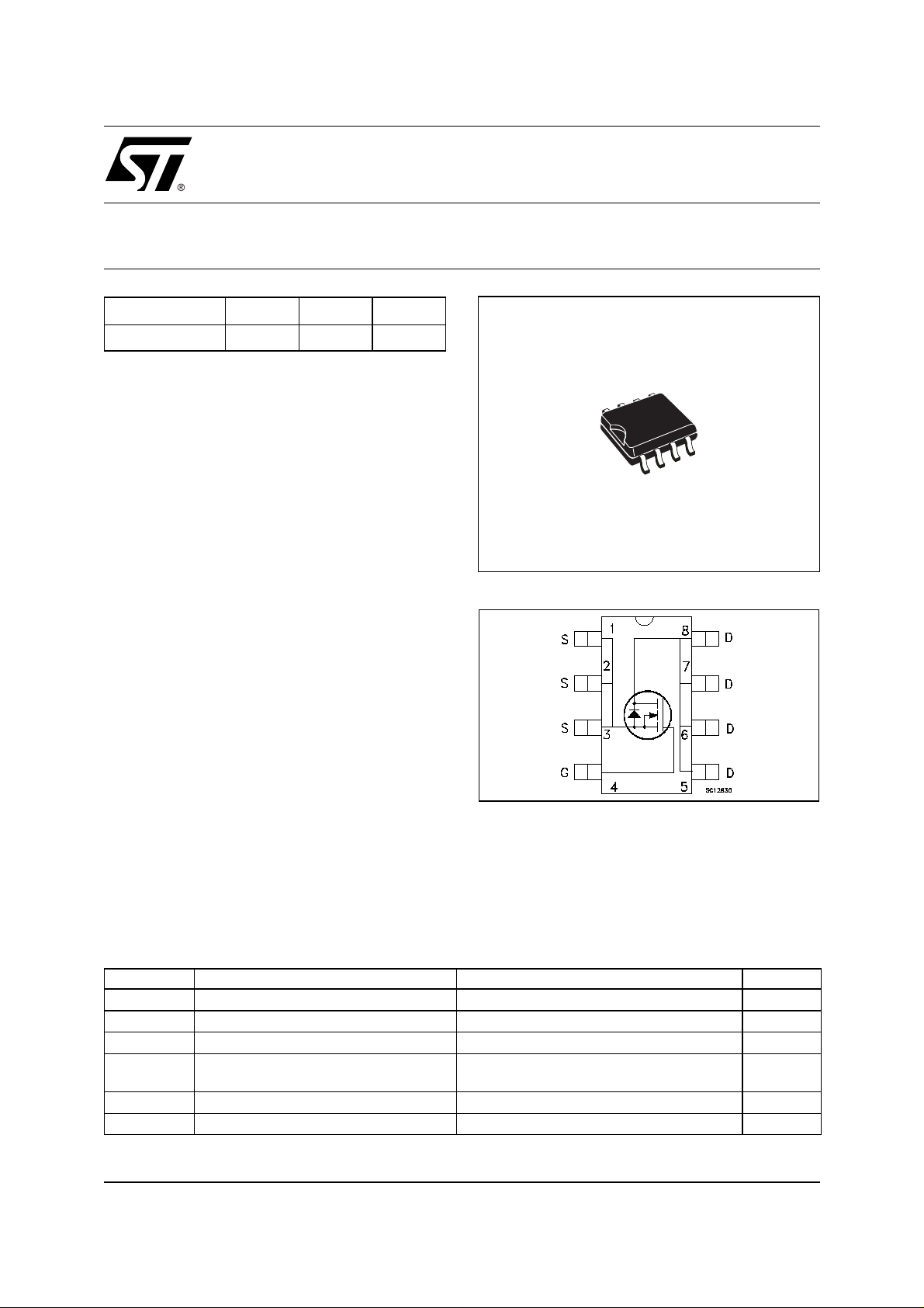
SO-8
INTERNAL SCHEMATIC DIAGRAM
ABSOLUTE MAXIMUM RATINGS
Symbol Parameter Value Unit
V
DS
V
DGR
V
GS
I
D
I
(
DM
P
tot
(
Pulse widt h l i m i ted by safe o perating area.
•)
.
Drain-source Voltage (VGS = 0)
Drain-gate Voltage (RGS = 20 kΩ)
100 V
100 V
Gate- source Voltage ± 20 V
Drain Current (continuos) at TC = 25°C
Drain Current (continuos) at T
•)
Drain Current (pulsed) 16 A
= 100°C
C
Total Dissipation at TC = 25°C
4
2.5
2.5 W
A
A
1/8July 2001
Page 2
STS4NF100
THERMAL DATA
Rthj-amb
T
T
stg
(*)
Mounte d on F R-4 board (t [ 10 se c.)
(*)Thermal Resistance Junction-ambient Single Operatio
Thermal Operating Junction-ambient
j
Storage Temperature
50
-55 to 150
-55 to 150
°C/W
°C
°C
ELECTRICAL CHARACTERISTICS (T
= 25 °C unless otherwise specified)
case
OFF
Symbol Parameter Test Conditions Min. Typ. Max. Unit
I
V
(BR)DSS
Drain-source
= 250 µA, VGS = 0
D
100 V
Breakdown Voltage
V
= Max Rating
DS
V
= Max Rating TC = 125°C
DS
V
= ± 20 V
GS
1
10
±100 nA
ON
(*)
I
DSS
I
GSS
Zero Gate Voltage
Drain Current (V
GS
Gate-body Leakage
Current (V
DS
= 0)
= 0)
Symbol Parameter Test Conditions Min. Typ. Max. Unit
V
GS(th)
R
DS(on)
Gate Threshold Voltage
Static Drain-source On
= VGS I
DS
V
= 10 V ID = 2 A
GS
= 250 µA
D
234V
0.065 0.070
V
Resistance
DYNAMIC
Symbol Parameter Test Conditions Min. Typ. Max. Unit
(*)
g
fs
C
iss
C
oss
C
rss
Forward Transconductance
Input Capacitance
Output Capacitance
Reverse Transfer
Capacitance
V
DS>ID(on)xRDS(on)max ID
= 25V, f = 1 MHz, VGS = 0
V
DS
=2 A
10 S
870
125
52
µA
µA
Ω
pF
pF
pF
2/8
Page 3
STS4NF100
ELECTRICAL CHARACTERISTICS (continued)
SWITCHING ON
Symbol Parameter Test Conditions Min. Typ. Max. Unit
= 50 V ID = 4 A
t
d(on)
Turn-on Delay Time
t
r
Rise Time
V
DD
R
= 4.7 Ω VGS = 10 V
G
(Resistive Load, Figure 3)
Q
g
Q
gs
Q
gd
Total Gate Charge
Gate-Source Charge
Gate-Drain Charge
= 80V ID= 4A VGS=10V
V
DD
SWITCHING OFF
Symbol Parameter Test Conditions Min. Typ. Max. Unit
= 50 V ID = 4 A
t
d(off)
Turn-off Delay Time
t
f
Fall Time
V
DD
R
= 4.7Ω, V
G
GS
= 10 V
(Resistive Load, Figure 3)
SOURCE DRAIN DIODE
Symbol Parameter Test Conditions Min. Typ. Max. Unit
I
SD
I
SDM
V
SD
t
rr
Q
rr
I
RRM
(*)
Pulsed: P ul se duration = 300 µs, duty cycle 1.5 %.
(
•)Pulse width limited by s afe operating area.
Source-drain Current
(•)
Source-drain Current (pulsed)
(*)
Forward On Voltage
Reverse Recovery Time
Reverse Recovery Charge
Reverse Recovery Current
I
= 4 A VGS = 0
SD
= 4 A di/dt = 100A/µs
I
SD
V
= 30 V Tj = 150°C
DD
(see test circuit, Figure 5)
58
45
30
6
10
49
17
100
375
7.5
41 nC
4
16
1.2 V
ns
ns
nC
nC
ns
ns
A
A
ns
nC
A
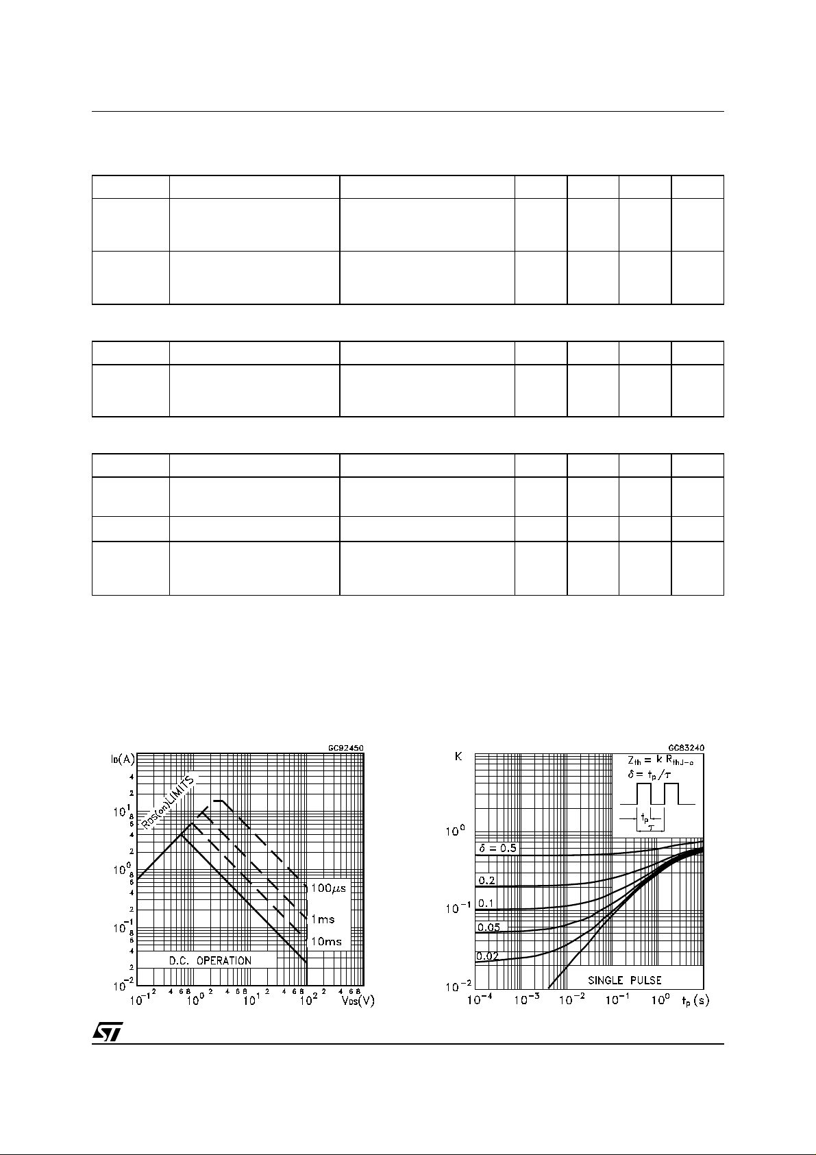
Safe Operating Area
Thermal Impedance
3/8
Page 4

STS4NF100
Output Characteristics Transfer Characteristics
Transconductance Static Drain-source On Resistance
Gate Charge vs Gate-source Voltage Capacitance Variations
4/8
Page 5

Normalized Gate Threshold Voltage vs Temperature Normalized on Resistance vs Temperature
Source-drain Diode Forward Characteristics .
STS4NF100
. .
5/8
Page 6

STS4NF100
Fig. 1: Unclamped Inductive Load Test CircuitFig. 1: Unclamped Inductive Load Test Circuit Fig. 2: Unclamped Inductive Waveform
Fig. 3: Switching Times Test Circuits For Resistive
Load
Fig. 5: Test Circuit For Inductive Load Switching
And Diode Recovery Times
Fig. 4: Gate Charge test Circuit
6/8
Page 7

SO-8 MECHANICAL DATA
STS4NF100
DIM.
MIN. TYP. MAX. MIN. TYP. MAX.
A1.750.068
a1 0.1 0.25 0.003 0.009
a2 1.65 0.064
a3 0.65 0.85 0.025 0.033
b 0.35 0.48 0.013 0.018
b1 0.19 0.25 0.007 0.010
C 0.25 0.5 0.010 0.019
c1 45 (typ.)
D 4.8 5.0 0.188 0.196
E 5.8 6.2 0.228 0.244
e1.27 0.050
e3 3.81 0.150
F 3.8 4.0 0.14 0.157
L 0.4 1.27 0.015 0.050
M0.60.023
S 8 (max.)
mm inch
0016023
7/8
Page 8

STS4NF100
Information furnished is believed to be accurate an d rel i able. Howev er, STMicroel ectronics assumes no resp onsibility for the consequence s
of use of such information nor for any infringement of patents or other rights of third parties which may result from its use. No license is granted
by implic ation or otherwise under any patent or patent rights of STMi croelectr onics. Sp ecifications mentioned in thi s publicati on are subject
to change without notice. This publication supersedes and replaces all information previously supplied. STMicroelectronics products are not
authorized for use as cri tical comp onents in life support dev i ces or systems wi thout exp ress written approval of STM i croelect ronics.
The ST log o i s registered trademark of STMicroelectronics
2001 STMi croelectr onics - All Rights Rese rved
All other names are the property of their respective owners.
Australi a - Brazil - Chi na - Finland - F rance - Germ any - Hong Kong - India - Italy - Japan - Malaysia - Malta - Morocco -
Singapor e - Spain - Sweden - Switzerl and - Unit ed K i ngdom - U.S. A.
STMicroelect ro n ics GRO UP OF COMPANI ES
http://www.st.com
8/8
 Loading...