

Page 1

STripFET™ II MOSFET PLUS SCHOTTKY RECTIFIER
MAIN PRODUCT CHARACTERISTICS
MOSFET
V
DSS
30 V < 0.055 Ω 4 A
R
DS(on)
STS4DNFS30L
N-CHANNEL 30V - 0.044Ω - 4A SO-8
I
D
SCHOTTKY
I
F(AV )
3 A 30 V 0.51 V
V
RRM
V
F(MAX)
SO-8
DESCRIPTION
This product associates the latest low voltage
STripFET™ in n-channel version to a low drop
INTERNAL SCHEMATIC DIAGRAM
Schottky diode. Such configuration is extremely versatile in implementing, a large variety of DC-DC
converters for printers, portable equipment, and cellular phones.
MOSFET ABSOLUTE MAXIMUM RATINGS
Symbol Parameter Value Unit
V
DS
V
DGR
V
GS
I
D
I
D
I
(●)
DM
P
TOT
Drain-source Voltage (VGS = 0)
Drain-gate Voltage (RGS = 20 kΩ)
Gate- source Voltage ± 16 V
Drain Current (continuous) at TC = 25°C
Drain Current (continuous) at TC = 100°C
Drain Current (pulsed) 16 A
Total Dissipation at TC = 25°C
30 V
30 V
4A
2.5 A
2W
SCHOTTKY ABSOLUTE MAXIMUM RATINGS
Symbol Parameter Value Unit
V
RRM
I
F(RMS)
I
F(AV)
I
FSM
I
RRM
I
RSM
dv/dt
(•)Pu l se width limite d by safe operating area
Repetitive Peak Reverse Voltage 30 V
RMS Forward Current 20 A
Average Forward Current TL = 125°C
Surge Non Repetitive Forward Current tp = 10 ms
Repetitive Peak Reverse Current tp = 2 µs
Non Repetitive Peak Reverse Current
Critical Rate Of Rise Of Reverse Voltage 10000 V/µs
δ = 0.5
Sinusoidal
F=1 kHz
tp = 100 µs1 A
3A
75 A
1A
1/8July 2002
Page 2

STS4DNFS30L
THERMA L D ATA
Rthj-amb (*)Thermal Resistance Junction-ambient MOSFET 62.5 °C/W
T
stg
T
l
MOSFET ELECTRICAL CHARACTERISTICS (TCASE = 25 °C UNLESS OTHERWISE SPECIFIED)
OFF
Symbol Parameter Test Conditions Min. Typ. Max. Unit
V
(BR)DSS
I
DSS
I
GSS
ON (1)
Symbol Parameter Test Conditions Min. Typ. Max. Unit
V
GS(th)
R
DS(on)
Storage Temperature Range -55 to 150 °C
Junction Temperature -55 to 150 °C
(*) Mounted on FR-4 bo ard (Steady State)
Drain-source
ID = 250 µA, VGS = 0 30 V
Breakdown Voltage
Zero Gate Voltage
Drain Current (V
GS
= 0)
Gate-body Leakage
Current (V
DS
= 0)
Gate Threshold Voltage
Static Drain-source On
Resistance
V
= Max Rating
DS
V
= Max Rating, TC = 125 °C
DS
V
= ± 16 V ±100 nA
GS
V
= VGS, ID = 250µA
DS
VGS = 10V, ID = 2 A
VGS = 5V, ID = 2 A
1V
0.044 0.055 Ω
0.051 0.065 Ω
1µA
10 µA
DYNAMIC
Symbol Parameter Test Conditions Min. Typ. Max. Unit
(1) Forward Transconductance VDS = 15 V
g
fs
C
iss
C
oss
C
rss
Input Capacitance
Output Capacitance 90 pF
Reverse Transfer
V
DS
Capacitance
= 25V, f = 1 MHz, VGS = 0
=2 A 5 S
, ID
330 pF
40 pF
2/8
Page 3
STS4DNFS30L
ELECTRICAL CHARACTERISTICS (CONTINUED)
1.
SWITCHING ON
Symbol Parameter Test Conditions Min. Typ. Max. Unit
V
t
d(on)
Q
Q
Q
t
r
gs
gd
Turn-on Delay Time
Rise Time 100 ns
Total Gate Charge
g
Gate-Source Charge 3.6 nC
Gate-Drain Charge 2 nC
SWITCHING OFF
Symbol Parameter Test Conditions Min. Typ. Max. Unit
t
d(off)
t
f
Turn-off Delay Time
Fall Time
SOURCE DRAIN DIODE
Symbol Parameter Test Conditions Min. Typ. Max. Unit
I
SD
I
SDM
VSD (1)
t
rr
Q
rr
I
RRM
Note: 1. Pulsed: Pu l se duration = 300 µs, duty cyc l e 1.5 %.
2. Pulse width li mited by safe operating area.
Source-drain Current 4 A
(2)
Source-drain Current (pulsed) 16 A
Forward On Voltage
Reverse Recovery Time
Reverse Recovery Charge 25 nC
Reverse Recovery Current 1.4 A
= 15 V, ID = 2 A
DD
R
= 4.7 Ω VGS = 5 V
G
(see test circuit, Figure 1)
V
= 24 V, ID = 4 A,
DD
VGS = 5 V
VDD = 15 V, ID = 2 A,
RG=4.7Ω, V
GS
= 5 V
(see test circuit, Figure 1)
ISD = 4 A, VGS = 0
I
= 4 A, di/dt = 100A/µs,
SD
V
= 15 V, Tj = 150°C
DD
(see test circuit, Figure 3)
11 ns
6.5 9 nC
25
22
1.2 V
35 ns
ns
ns
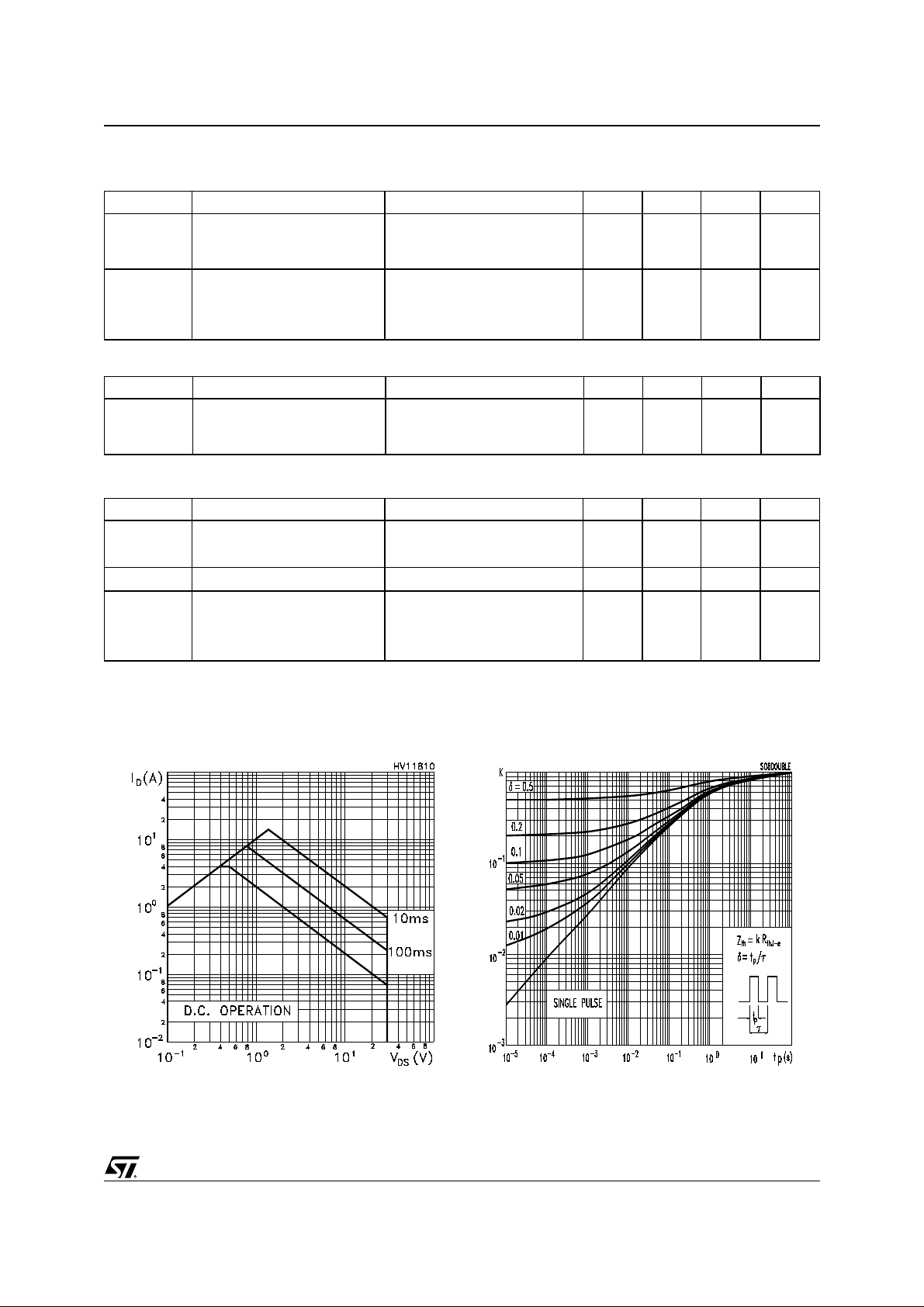
Safe Operating Area
Thermal Impedance
3/8
Page 4

STS4DNFS30L
Output Characteristics Transfer Characteristics
Transconductance
Gate Charge vs Gate-source Voltage
Static Drain-source On Resistance
Capacitance Variations
4/8
Page 5

STS4DNFS30L
Normalized Gate Thereshold Voltage vs Temp. Normalized On Resistance vs Temperature
Source-drain Diode Forward Characteristics
5/8
Page 6

STS4DNFS30L
Resistive Load
Fig. 3: Test Circuit For Diode Recovery Behaviour
Fig. 2: Gate Charge test CircuitFig. 1: Switching Times Test Circuit For
6/8
Page 7

SO-8 MECHANICAL DATA
STS4DNFS30L
DIM.
MIN. TYP. MAX. MIN. TYP. MAX.
A1.750.068
a1 0.1 0.25 0.003 0.009
a2 1.65 0.064
a3 0.65 0.85 0.025 0.033
b 0.35 0.48 0.013 0.018
b1 0.19 0.25 0.007 0.010
C 0.25 0.5 0.010 0.019
c1 45 (typ.)
D 4.8 5.0 0.188 0.196
E 5.8 6.2 0.228 0.244
e1.27 0.050
e3 3.81 0.150
F 3.8 4.0 0.14 0.157
L 0.4 1.27 0.015 0.050
M0.60.023
S 8 (max.)
mm inch
0016023
7/8
Page 8

STS4DNFS30L
Information furnished is believed to be accurate and reliable. However, STMicroelectronics assumes no responsibilit y for the
consequences of use of su ch in formation nor for any in fringement of patents or other rights of third parties w hich may result from
its use. No license is granted by implication or otherwise under any patent or patent rights of STMicroelectronics. Specifications
mentioned in this publication are subject to change without notice. This publication supersedes and replaces all information
previously suppli ed. STMi croelect ronics pr oducts are not author ized for use as cr itical component s in li fe suppo rt devi ces or
systems without express written approval of STMicroelectronics.
Australia - Brazil - Canada - China - Finland - France - Germany - Hong Kong - India - Israel - Italy - Japan - Malaysia - Malta - Morocco
© The ST logo is a registered trademark of STMicroelectronics
© 2002 STMicroelectronics - Printed in Italy - All Rights Reserved
Singapore - Spain - Sweden - Switzerland - United Kingdom - United States.
STMicroelectronics GROUP OF COMPANIES
© http://www.st.com
8/8
 Loading...