

Page 1
STS25NH3LL
N-CHANNEL 30V - 0.0032 Ω - 25A SO-8
STripFET™ III MOSFET FOR DC-DC CONVERSION
TYPE
V
DSS
STS25NH3LL 30 V <0.0035
■ TYPICAL R
■ OPTIMAL R
■ CONDUCTION LOSSES REDUCED
■ SWITCHING LOSSES REDUCED
(on) = 0.0032 Ω @ 10V
DS
(on) x Qg TRADE-OFF @ 4.5V
DS
R
DS(on)
I
D
25 A
Ω
DESCRIPTION
The STS25NH3LL utilizes the latest advanced design
rules of ST's propetary STripFET™ technology. This
novel 0.6µ process coupled to unique metalization
techniques re alizes the most advanced low voltage
MOSFET in SO- 8 eve r pro duced . It is there fore s uit ab le
for the most demanding DC-DC converter applications
where high efficiency is to be achived at high output
current.
APPLICATIONS
■ DC-DC CONVERTERS FOR TELECOM AND
NOTEBOOK CPU CORE
■ SYNCHRONOUS RECTIFIER
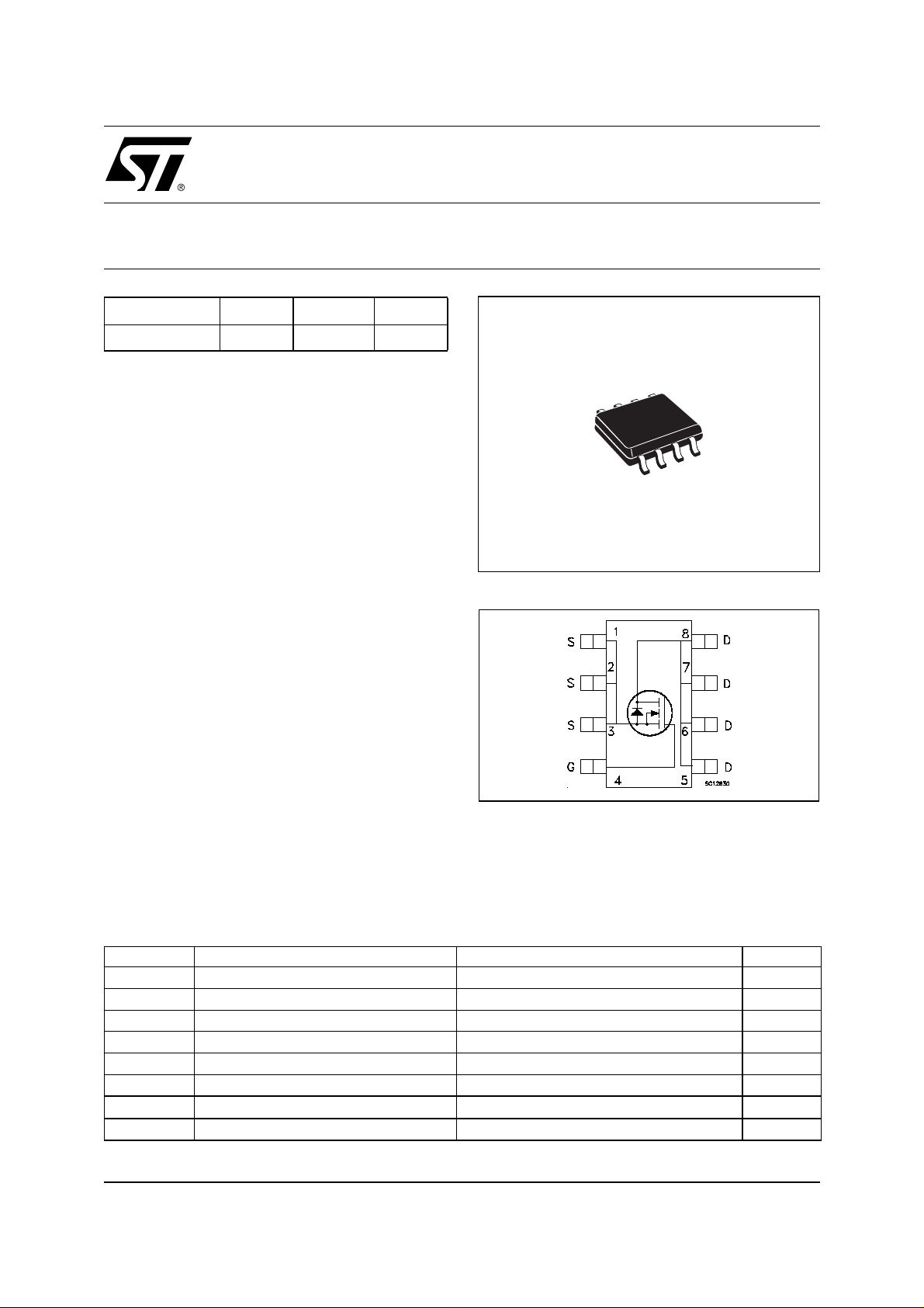
SO-8
INTERNAL SCHEMATIC DIAGRAM
ABSOLUTE MAXIMUM RATINGS
Symbol Parameter Value Unit
V
DS
V
DGR
V
GS
I
D
I
D
(
I
DM
E
AS
P
tot
(
Pulse widt h l i m i ted by safe operating area.
•)
.
Drain-source Voltage (VGS = 0)
Drain-gate Voltage (RGS = 20 kΩ)
30 V
30 V
Gate- source Voltage ± 18 V
Drain Current (continuous) at TC = 25°C
Drain Current (continuous) at TC = 100°C
•)
Drain Current (pulsed) 100 A
(1)
Single Pulse Avalanche Energy 200 mJ
Total Dissipation at TC = 25°C
(1)
Starting Tj = 25 oC ID = 12.5A VDD = 30V
25 A
18 A
3.2 W
1/8September 2003
Page 2
STS25NH3LL
THERMA L D ATA
Rthj-amb
Rthj-lead
T
T
stg
(*)
When Mounted on 1 inch2 FR-4 board, 2 oz of Cu and t [ 10 sec.
(*)
Thermal Resistance Junction-ambient
Thermal Resistance Junction-leads
Maximum Operating Junction Temperature
j
Storage Temperature
Max
Max
47
16
-55 to 175
-55 to 175
°C/W
°C/W
°C
°C
ELECTRICAL CHARACTERISTICS (T
= 25 °C unless otherwise specified)
case
OFF
Symbol Parameter Test Conditions Min. Typ. Max. Unit
I
= 250 µA, VGS = 0
D
V
= Max Rating
DS
V
= Max Rating TC = 125°C
DS
V
= ± 18 V
GS
30 V
1
10
±100 nA
ON
V
(BR)DSS
I
DSS
I
GSS
(*)
Drain-source
Breakdown Voltage
Zero Gate Voltage
Drain Current (V
GS
Gate-body Leakage
Current (V
DS
= 0)
= 0)
Symbol Parameter Test Conditions Min. Typ. Max. Unit
V
V
GS(th)
R
DS(on)
Gate Threshold Voltage
Static Drain-source On
Resistance
= VGS I
DS
= 10 V ID = 12.5 A
V
GS
V
= 4.5 V ID = 12.5 A
GS
= 250 µA
D
1V
0.0032
0.004
0.0035
0.005
DYNAMIC
Symbol Parameter Test Conditions Min. Typ. Max. Unit
(*)
g
fs
C
iss
C
oss
C
rss
Forward Transconductance
Input Capacitance
Output Capacitance
Reverse Transfer
Capacitance
V
= 10 V ID= 12.5 A
DS
= 25V, f = 1 MHz, VGS = 0
V
DS
30 S
4450
655
50
µA
µA
Ω
Ω
pF
pF
pF
2/8
Page 3

STS25NH3LL
ELECTRICAL CHARACTERISTICS (continued)
SWITCHING ON
Symbol Parameter Test Conditions Min. Typ. Max. Unit
= 15 V ID = 12.5 A
t
d(on)
Turn-on Delay Time
t
r
Rise Time
V
DD
R
= 4.7 Ω VGS = 10 V
G
(Resistive Load, Figure 1)
Q
g
Q
gs
Q
gd
Total Gate Charge
Gate-Source Charge
Gate-Drain Charge
=15V ID=25A VGS=4.5 V
V
DD
(see test circuit, Figure 2)
SWITCHING OFF
Symbol Parameter Test Conditions Min. Typ. Max. Unit
= 15 V ID = 12.5 A
t
d(off)
Turn-off Delay Time
t
f
Fall Time
V
DD
R
= 4.7Ω, V
G
GS
= 10 V
(Resistive Load, Figure 3)
SOURCE DRAIN DIODE
Symbol Parameter Test Conditions Min. Typ. Max. Unit
I
SD
I
SDM
V
SD
t
rr
Q
rr
I
RRM
(*)
Pulsed: P ul se duration = 300 µs, duty cycle 1.5 %.
(
•)Pulse width limited by s afe operating area.
Source-drain Current
Source-drain Current (pulsed)
(*)
Forward On Voltage
Reverse Recovery Time
Reverse Recovery Charge
Reverse Recovery Current
I
= 25 A VGS = 0
SD
= 25 A di/dt = 100A/µs
I
SD
V
= 25 V Tj = 150°C
DD
(see test circuit, Figure 3)
18
50
30
12.5
10
75
8
32
34
2.1
40 nC
25
100
1.2 V
ns
ns
nC
nC
ns
ns
A
A
ns
nC
A
Safe Operating Area
Thermal Impedance
3/8
Page 4

STS25NH3LL
Output Characteristics Transfer Characteristics
Transconductance Static Drain-source On Resistance
Gate Charge vs Gate-source Voltage Capacitance Variations
4/8
Page 5

STS25NH3LL
Normalized Gate Threshold Voltage vs Temperature Normalized on Resistance vs Temperature
Source-drain Diode Forward Characteristics Normalized Breakdown Voltage vs Temperature.
. .
. .
5/8
Page 6

STS25NH3LL
Fig. 1: Switching Times Test Circuits For Resistive
Load
Fig. 3: Test Circuit For Diode Recovery Behaviour
Fig. 2: Gate Charge test Circuit
6/8
Page 7

SO-8 MECHANICAL DATA
STS25NH3LL
DIM.
MIN. TYP. MAX. MIN. TYP. MAX.
A1.750.068
a1 0.1 0.25 0.003 0.009
a2 1.65 0.064
a3 0.65 0.85 0.025 0.033
b 0.35 0.48 0.013 0.018
b1 0.19 0.25 0.007 0.010
C 0.25 0.5 0.010 0.019
c1 45 (typ.)
D 4.8 5.0 0.188 0.196
E 5.8 6.2 0.228 0.244
e1.27 0.050
e3 3.81 0.150
F 3.8 4.0 0.14 0.157
L 0.4 1.27 0.015 0.050
M0.60.023
S 8 (max.)
mm inch
0016023
7/8
Page 8

STS25NH3LL
Information furnished is believed to be accurate and reliable. However, STMicroelectronics assumes no responsibility for the consequences
of use of such information nor for any infringement of patents or other rights of third parties which may result from its use. No license is granted
by implic ation or otherwise under any patent or patent r i ght s of STMi croelectr oni cs. Spec i fications mentione d i n this publicatio n are subj ect
to change without notice. This publication supersedes and replaces all information previously supplied. STMicroelectronics product s are not
authorized for use as cri tical comp onents in lif e support devi ces or systems without express written approva l of STMicroe l ectronics.
The ST logo is registered trademark of STMicroelectronics
2003 STMi croelectronics - All Ri ghts Rese rved
All other na m es are the property of their respective owners.
Australi a - Brazil - Canada - Chin a - F i nland - France - German y - Hong Kong - I ndia - Israel - It al y - Japan - Malaysia - Mal ta - Morocco -
Singap ore - Spain - Sw eden - Switzerland - Uni ted Kingdom - United St at es.
STMicroelectronics GROUP OF COMPANIES
http:// www.st.com
8/8
 Loading...