

Page 1
STS1DNC45
DUAL N-CHANNEL 450V - 4.1Ω -0.4ASO-8
SuperMESH™ POWER MOSFET
TYPE V
DSS
R
DS(on)
I
D
STS1DNC45 450 V < 4.5 Ω 0.4 A
■ TYPICAL R
■ STANDARD OUTLINE FOR EASY
(on) = 4.1Ω
DS
AUTOMATED SURFACE MOUNT ASSEMBLY
■ GATE CHARGE MINIMIZED
DESCRIPTION
The SuperMESH™ series is obtained through an
extreme optimization of ST ’s well established stripbased PowerMESH™ layout. In addition to pus hing
on-resistance significantly down, s pec ial care is taken to ensure a very good dv/dt capability for the
most demanding app lications. Such series compl ements ST full range of high voltage MOSFETs including revolutionary MDm es h™ products.
APPLICATIONS
■ SWITCH MODE LOW POWER SUPPLIES
(SMPS)
■ DC-DC CONVERTERS
■ LOW POWER, LOW CO ST CFL (COMPACT
FLUORESCENT LAMPS)
■ LOW POWER BATTERY CHA RGERS
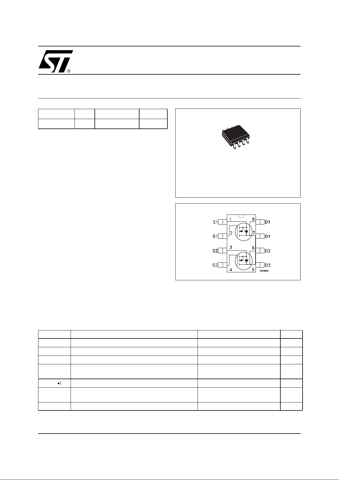
SO-8
INTERNAL SCHEMATIC DIAGRAM
ABSOLUTE MAXIMUM RATINGS
Symbol Parameter Value Unit
V
DS
V
DGR
V
GS
I
D
I
DM
P
TOT
dv/dt(1) Peak Diode Recovery voltage slope 3 V/ns
(●) Pulse width limited by safe operating area
Drain-source Voltage (VGS=0)
Drain-gate Voltage (RGS=20kΩ)
450 V
450 V
Gate- source Voltage ± 30 V
Drain Current (continuous) at TC= 25°C
Drain Current (continuous) at TC= 100°C
()
Drain Current (pulsed) 1.6 A
Total Dissipation at TC= 25°C Dual Operation
Total Dissipation at TC= 25°C Single Operation
(1)ISD≤ 0.4 A, di/dt ≤100A/µs, VDD≤ V
0.40
0.25
1.6
2
(BR)DSS,Tj≤TJMAX.
A
A
W
W
1/8June 2003
Page 2
STS1DNC45
THERMAL DATA
Rthj-amb(#) Thermal Resistance Junction-ambient Max Single Operation
Thermal Resistance Junction-ambient Max Dual Operation
T
j
T
stg
(#) When Mounted on FR4 board (Steady State)
Max. Operating Junction Temperature 150 °C
Storage Temperature –65 to 150 °C
AVALANCHE CHARACTERISTICS
Symbol Parameter Max Value Unit
I
AR
E
AS
Avalanche Current, Repetitive or Not-Repetitive
(pulse width limited by T
max)
j
Single Pulse Avalanche Energy
(starting T
= 25 °C, ID=IAR,VDD=50V)
j
62.5
78
0.4 A
30 mJ
°C/W
°C/W
ELECTRICAL CHARACTERISTICS (T
= 25 °C UNLESS OTHERWISE SPECIFIED)
CASE
OFF
Symbol Parameter Test Conditions Min. Typ. Max. Unit
V
(BR)DSS
Drain-source
ID= 250 µA, VGS= 0 450 V
Breakdown Voltage
I
DSS
I
GSS
Zero Gate Voltage
Drain Current (V
GS
Gate-body Leakage
Current (V
DS
=0)
=0)
V
= Max Rating
DS
= Max Rating, TC= 125 °C
V
DS
V
= ± 30V ±100 nA
GS
1µA
50 µA
ON (1)
Symbol Parameter Test Conditions Min. Typ. Max. Unit
V
GS(th)
R
DS(on)
Gate Threshold Voltage
Static Drain-source On
V
DS=VGS,ID
VGS=10V,ID= 0.5 A
= 250µA
2.3 3 3.7 V
4.1 4.5 Ω
Resistance
DYNAMIC
Symbol Parameter Test Conditions Min. Typ. Max. Unit
(1) Forward Transconductance VDS=25V,ID= 0.5 A 1.1 S
g
fs
C
iss
C
oss
C
rss
Input Capacitance
Output Capacitance 27.5 pF
Reverse Transfer
Capacitance
V
=25V,f=1MHz,VGS=0
DS
160 pF
4.7 pF
2/8
Page 3
STS1DNC45
ELECTRICAL CHARACTERISTICS (CONTINUED)
SWITCHING ON
Symbol Parameter Test Conditions Min. Typ. Max. Unit
V
t
d(on)
Q
Q
Q
t
r
g
gs
gd
Turn-on Delay Time
Rise Time 4 ns
Total Gate Charge
Gate-Source Charge
Gate-Drain Charge
SWITCHING OFF
Symbol Parameter Test Conditions Min. Typ. Max. Unit
t
r(off)
t
f
t
c
Off-voltage Rise Time
Fall Time
Cross-over Time
SOURCE DRAIN DIODE
Symbol Parameter Test Conditions Min. Typ. Max. Unit
I
SD
I
SDM
VSD(1)
t
rr
Q
rr
I
RRM
Note: 1. Pulsed: Pulse duration = 300 µs, duty cycle 1.5 %.
2. Pulse width limited by safe operating area.
Source-drain Current 0.4 A
(2)
Source-drain Current (pulsed) 1.6 A
Forward On Voltage
Reverse Recovery Time
Reverse Recovery Charge
Reverse Recovery Current
=225V,ID= 0.5 A
DD
= 4.7Ω VGS=10V
R
G
(see test circuit, Figure 3)
VDD=360V,ID= 1.5 A,
V
=10V
GS
= 360 V, ID= 1.5 A
V
DD
RG=4.7Ω, VGS=10V
(see test circuit, Figure 5)
ISD= 0.4 A, VGS=0
= 0.4 A, di/dt = 100A/µs,
I
SD
VDD=100V,Tj=150°C
(see test circuit, Figure 5)
6.7 ns
7
10 nC
1.3
3.2
8.5
12
18
1.6 V
225
530
4.7
nC
nC
ns
ns
ns
ns
nC
A
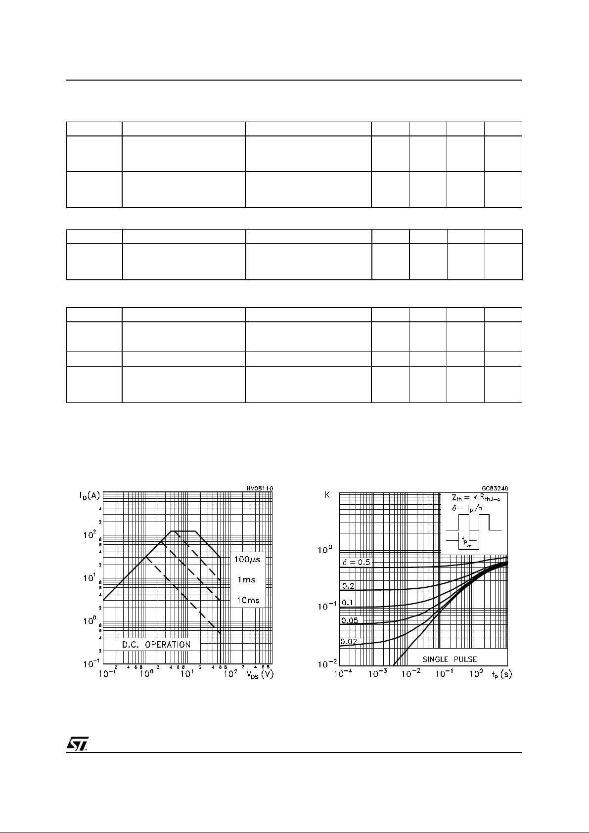
Safe Operating Area Thermal Im pedance
3/8
Page 4

STS1DNC45
Output Characteristics
Transconductance Static Drain-source On Resistance
Transfer Characteristics
Gate Charge vs Gate-so urce Voltage
4/8
Capacitance Variations
Page 5

STS1DNC45
Normalized Gate Threshold Voltage vs Temp. Normalized On Resistance vs Temperature
Source-drain Dio de Forward Char acteristics
Max Id Current vs Tc
Normalized BVDSS vs Temperature
Maximum Avalanche Energy vs Temperature
5/8
Page 6

STS1DNC45
Fig. 2: Unclamped Induc tive WaveformFig. 1: Unclamped In duc tive Load Test Circuit
Fig. 3: Switching Times Test Circuit For
Resistive Load
Fig. 5: Test Circuit For Inductive Load Switching
And Diode Recovery Times
Fig. 4: Gate Charge test Circuit
6/8
Page 7

0016023
SO-8 MECHANICAL DATA
STS1DNC45
DIM.
MIN. TYP. MAX. MIN. TYP. MAX.
A1.750.068
a1 0.1 0.25 0.003 0.009
a2 1.65 0.064
a3 0.65 0.85 0.025 0.033
b 0.35 0.48 0.013 0.018
b1 0.19 0.25 0.007 0.010
C 0.25 0.5 0.010 0.019
c1 45 (typ.)
D 4.8 5.0 0.188 0.196
E 5.8 6.2 0.228 0.244
e1.27 0.050
e3 3.81 0.150
F 3.8 4.0 0.14 0.157
L 0.4 1.27 0.015 0.050
M0.60.023
S 8 (max.)
mm inch
7/8
Page 8

STS1DNC45
Information furnished is believed to be accurate and reliable. However, STMicroelectronics assumes no responsibility for the
consequences of u se of such inform ation nor for any in fring ement of p atents or o ther ri ghts of th ird p arties which may r esul t f rom
its use. No license is granted by implication or otherwise under any patent or patent rights of STMicroelectronics. Specifications
mentioned in this publication are subject to change without notice. This publication supersedes and replaces all information
previously supplied. STMicroelectronics products are not authorized for use as critical components in life support devices or
systems without express written approval of STMicroelectronics.
Australia - Brazil - Canada - China - Finland - France - Germany - Hong Kong - India - Israel - Italy - Japan - Malaysia - Malta - Morocco
© The ST logo is a registered trademark of STMicroelectronics
© 2003 STMicroelectronics - Printed in Italy - All Rights Reserved
Singapore - Spain - Sweden - Switzerland - United Kingdom - United States.
STMicroelectronics GROUP OF COMPANIES
© http://www.st.com
8/8
 Loading...