

Page 1
STS17NF3LL
N-CHANNEL 30V - 0.0045 Ω - 17A SO-8
STripFET™ II MOSFET FOR DC-DC CONVERSION
TYPE
STS17NF3LL 30 V <0.0055
■ TYPICAL R
■ OPTIMAL R
■ CONDUCTION LOSSES REDUCED
■ SWITCHING LOSSES REDUCED
V
DSS
(on) = 0.0045 Ω @ 10V
DS
(on) x Qg TRADE-OFF @ 4.5V
DS
R
DS(on)
I
D
17 A
Ω
DESCRIPTION
This application specific Power MOSFET is the
second generation of STMicroelectronis unique
"Single Feature Size™ " strip-based process. T he
resulting transistor shows the best trade-off
between on-resistance and gate charge. Such
features make it the best choice in high efficiency
DC-DC converters for Telecom and computer
industries.
APPLICATIONS
■ DC-DC CONVERTERS FOR TELECOM AND
NOTEBOOK CPU CORE
■ SYNCHRONOUS RECTIFIER
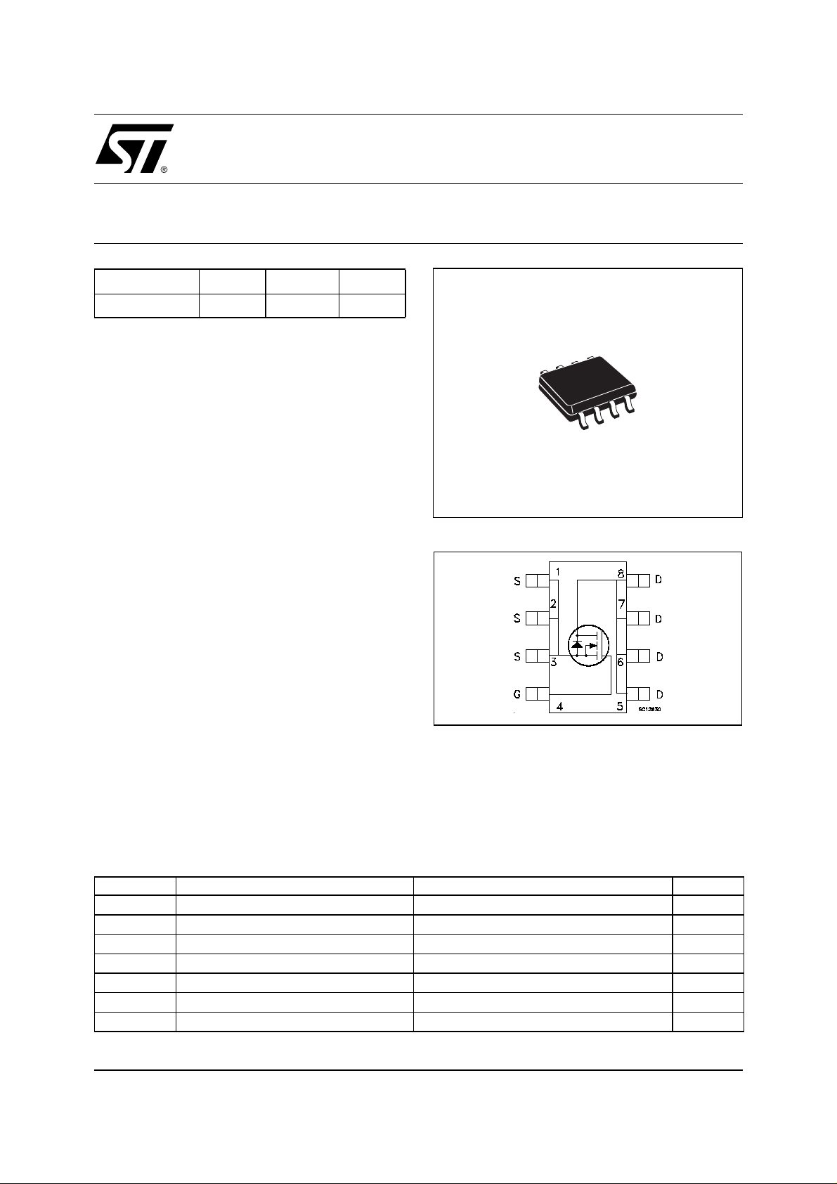
SO-8
INTERNAL SCHEMATIC DIAGRAM
ABSOLUTE MAXIMUM RATINGS
Symbol Parameter Value Unit
V
DS
V
DGR
V
GS
I
D
I
D
(
I
DM
P
tot
(
Pulse widt h l i m i ted by safe operating area.
•)
.
Drain-source Voltage (VGS = 0)
Drain-gate Voltage (RGS = 20 kΩ)
Gate- source Voltage ± 18 V
Drain Current (continuous) at TC = 25°C
Drain Current (continuous) at TC = 100°C
•)
Drain Current (pulsed) 68 A
Total Dissipation at TC = 25°C
30 V
30 V
17 A
12 A
3.2 W
1/8March 2003
Page 2
STS17NF3LL
THERMA L D ATA
Rthj-amb
Rthj-lead
T
T
stg
(*)
When Mounted on 1 inch2 FR-4 board, 2 oz of Cu and t [ 10 sec.
(*)
Thermal Resistance Junction-ambient
Thermal Resistance Junction-leads
Maximum Operating Junction Temperature
j
Storage Temperature
Max
Max
47
16
-55 to 175
-55 to 175
°C/W
°C/W
°C
°C
ELECTRICAL CHARACTERISTICS (T
= 25 °C unless otherwise specified)
case
OFF
Symbol Parameter Test Conditions Min. Typ. Max. Unit
I
= 250 µA, VGS = 0
D
V
= Max Rating
DS
V
= Max Rating TC = 125°C
DS
V
= ± 18 V
GS
30 V
1
10
±100 nA
ON
V
(BR)DSS
I
DSS
I
GSS
(*)
Drain-source
Breakdown Voltage
Zero Gate Voltage
Drain Current (V
GS
Gate-body Leakage
Current (V
DS
= 0)
= 0)
Symbol Parameter Test Conditions Min. Typ. Max. Unit
V
V
GS(th)
R
DS(on)
Gate Threshold Voltage
Static Drain-source On
Resistance
= VGS I
DS
= 10 V ID = 8.5 A
V
GS
V
= 4.5 V ID = 8.5 A
GS
= 250 µA
D
1V
0.0045
0.0055
0.0055
0.007
DYNAMIC
Symbol Parameter Test Conditions Min. Typ. Max. Unit
(*)
g
fs
C
iss
C
oss
C
rss
Forward Transconductance
Input Capacitance
Output Capacitance
Reverse Transfer
Capacitance
V
= 10 V ID= 8.5 A
DS
= 25V, f = 1 MHz, VGS = 0
V
DS
37 S
2160
614
98
µA
µA
Ω
Ω
pF
pF
pF
2/8
Page 3
STS17NF3LL
ELECTRICAL CHARACTERISTICS (continued)
SWITCHING ON
Symbol Parameter Test Conditions Min. Typ. Max. Unit
= 15 V ID = 8.5 A
t
d(on)
Turn-on Delay Time
t
r
Rise Time
V
DD
R
= 4.7 Ω VGS = 4.5 V
G
(Resistive Load, Figure 1)
Q
g
Q
gs
Q
gd
Total Gate Charge
Gate-Source Charge
Gate-Drain Charge
=24V ID=12.5A VGS=4.5 V
V
DD
(see test circuit, Figure 2)
SWITCHING OFF
Symbol Parameter Test Conditions Min. Typ. Max. Unit
= 15 V ID = 8.5 A
t
d(off)
Turn-off Delay Time
t
f
Fall Time
V
DD
R
= 4.7Ω, V
G
GS
= 4.5 V
(Resistive Load, Figure 3)
SOURCE DRAIN DIODE
Symbol Parameter Test Conditions Min. Typ. Max. Unit
I
SD
I
SDM
V
SD
t
rr
Q
rr
I
RRM
(*)
Pulsed: P ul se duration = 300 µs, duty cycl e 1. 5 %.
(
•)Pulse width limited by safe operatin g area.
Source-drain Current
(•)
Source-drain Current (pulsed)
(*)
Forward On Voltage
Reverse Recovery Time
Reverse Recovery Charge
Reverse Recovery Current
I
= 17 A VGS = 0
SD
= 17 A di/dt = 100A/µs
I
SD
V
= 15 V Tj = 150°C
DD
(see test circuit, Figure 3)
23.5
39
26
7
12
47.5
37
39
45
2.3
35 nC
17
68
1.2 V
ns
ns
nC
nC
ns
ns
A
A
ns
nC
A
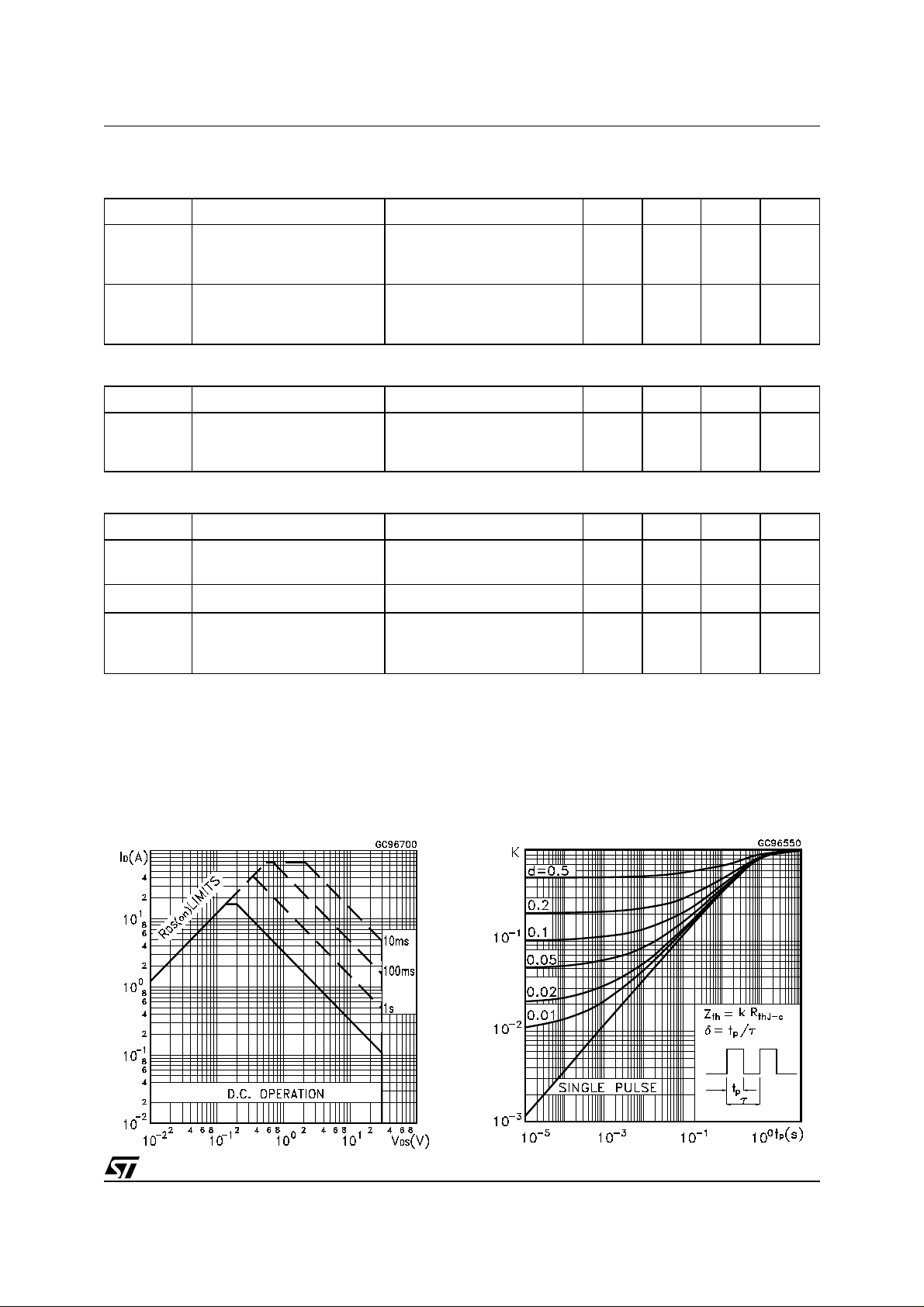
Safe Operating Area
Thermal Impedance
3/8
Page 4

STS17NF3LL
Output Characteristics Transfer Characteristics
Transconductance Static Drain-source On Resistance
Gate Charge vs Gate-source Voltage Capacitance Variations
4/8
Page 5

STS17NF3LL
Normalized Gate Threshold Voltage vs Temperature Normalized on Resistance vs Temperature
Source-drain Diode Forward Characteristics Normalized Breakdown Voltage vs Temperature.
. .
. .
5/8
Page 6

STS17NF3LL
Fig. 1: Switching Times Test Circuits For Resistive
Load
Fig. 3: Test Circuit For Diode Recovery Behaviour
Fig. 2: Gate Charge test Circuit
6/8
Page 7

SO-8 MECHANICAL DATA
STS17NF3LL
DIM.
MIN. TYP. MAX. MIN. TYP. MAX.
A1.750.068
a1 0.1 0.25 0.003 0.009
a2 1.65 0.064
a3 0.65 0.85 0.025 0.033
b 0.35 0.48 0.013 0.018
b1 0.19 0.25 0.007 0.010
C 0.25 0.5 0.010 0.019
c1 45 (typ.)
D 4.8 5.0 0.188 0.196
E 5.8 6.2 0.228 0.244
e1.27 0.050
e3 3.81 0.150
F 3.8 4.0 0.14 0.157
L 0.4 1.27 0.015 0.050
M0.60.023
S 8 (max.)
mm inch
0016023
7/8
Page 8

STS17NF3LL
Information furnished is believed to be accurate and reliable. However, STMicroelectronics assumes no responsibility for the consequences
of use of such information nor for any infringement of patents or other rights of third parties which may result from its use. No license is granted
by implic ation or oth erwise under any patent or patent rights of STMicroelectronic s. Specific ations mentioned in this public at ion ar e subject
to change without notice. This publication supersedes and replaces all information previously supplied. STMicroelectronics products are not
authorized for use as critical components in life support devi ces or systems wi thout express written ap proval of STMi croelectronics.
The ST logo is registered trademark of STMicroelectronics
2003 STMi croelectr oni cs - All Rights Reserved
All other na m es are the prop erty of their res pective owners.
Australi a - Brazil - Canada - China - F i nl and - France - Germany - Hong Kong - India - Israel - Italy - Japan - Malay sia - Malta - Morocco -
Singap ore - Spain - Sw eden - Switze rl and - United K i ngdom - Unit ed S tates.
STMicroelectronics GROUP OF COMPANIES
http:// www.st.com
8/8
 Loading...