

Page 1
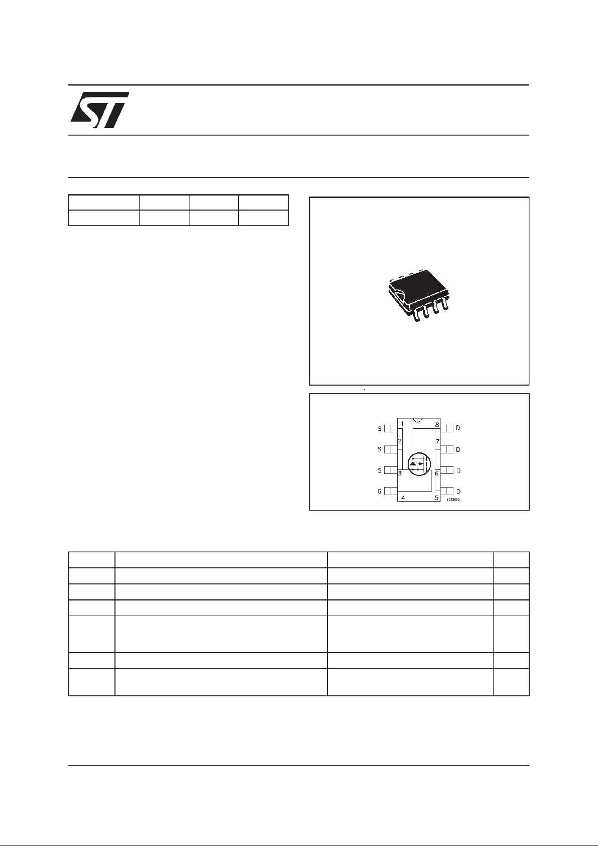
STS12NF30L
N - CHANNEL 30V - 0.0085Ω - 12A SO-8
STripFET POWER MOSFET
TYPE V
ST S12NF30L 30 V < 0 . 01 Ω 12 A
■ TYPICALR
■ STANDARD OUTLINEFOR EASY
DS(on)
DSS
= 0.0085 Ω
R
DS(on)
I
D
AUTOMATEDSURFACEMOUNTASSEMBLY
■ LOW THRESHOLDDRIVE
DESCRIPTION
This Power MOSFET is the second generation of
STMicroelectronics unique ” Single Feature
Size
”
strip-based process. The resulting
transistor shows extremely high packing density
for low on-resistance, rugged avalanche
characteristics and less critical alignment steps
therefore a remarkable manufacturing
reproducibility.
APPLICATIONS
■ DC MOTOR DRIVE
■ DC-DCCONVERTERS
■ BATTERYMANAGMENTIN NOMADIC
EQUIPMENT
■ POWERMANAGEMENT IN
PORTABLE/DESKTOPPC
s
SO-8
INTERNAL SCHEMATIC DIAGRAM
ABSOLUTE MAXIMUM RATINGS
Symb o l Parameter Value Unit
V
V
V
I
DM
P
(•) Pulse width limited by safeoperating area
May 1999
Drain-source Voltage (VGS=0) 30 V
DS
Drain- gat e Voltage (RGS=20kΩ)30V
DGR
Gate-s ource Voltage ± 20 V
GS
Drain Current (co nt inu ous ) at Tc = 25oC
I
D
Drain Current (co nt inu ous ) at T
(•) Drain Current (pulsed) 48 A
Tot al Dissipat ion at Tc=25oC 2.5 W
tot
=100oC
c
12
7.5
A
A
1/8
Page 2
STS12NF30L
THERMAL DATA
R
thj-amb
T
Tj
(*)T hermal R es istance Junction-am bie nt
Maximum O perating Juncti on Temperat ur e
stg
St orage Tempe ra tur e
50
150
-55 to 150
o
C/W
o
o
C
C
(*)
Mountedon FR-4board (t
ELECTRICAL CHARACTERISTICS (T
≤ 10
sec)
=25oC unless otherwisespecified)
case
OFF
Symbol Parameter Test Conditions Min. Typ. Max. Unit
V
(BR)DSS
Drain-source
ID=250µAVGS=0 30 V
Break dow n Volt age
I
DSS
I
GSS
Zero Gate Voltage
Drain Current (V
GS
Gat e- bod y Leakage
Current (V
DS
=0)
=0)
V
=MaxRating
DS
=MaxRating Tc=125oC
V
DS
V
=± 20 V
GS
1
10
100 nA
±
ON (∗)
Symbol Parameter Test Conditions Min. Typ. Max. Unit
V
GS(th)
R
DS(on)
I
D(on)
Gate Threshold Voltage VDS=VGSID= 250µA11.62.5V
Sta t ic Drain-sour c e On
Resistance
VGS=10V ID=6A
=4.5V ID=6A
V
GS
On State Drain Current VDS>I
D(on)xRDS(on )max
0.0085
0.01
12 A
0.01
0.012ΩΩ
VGS=10V
DYNAMIC
µA
µA
Symbol Parameter Test Conditions Min. Typ. Max. Unit
g
(∗)Forward
fs
VDS>I
D(on)xRDS(on )maxID
=6A 20 S
Tr ansc on duc tance
C
C
C
Input Capacit ance
iss
Out put Capacitance
oss
Reverse Transfer
rss
VDS=25V f=1MHz VGS= 0 V 2400
590
200
Capacit a nc e
2/8
pF
pF
pF
Page 3
STS12NF30L
ELECTRICAL CHARACTERISTICS
(continued)
SWITCHING ON
Symbol Parameter Test Conditions Min. Typ. Max. Unit
t
d(on)
Tur n-on Delay Time
Rise Time
t
r
VDD=15V ID=6A
R
=4.7
G
Ω
VGS=4.5V
35
90
(Resis t iv e Load, see f ig. 3 )
Q
Q
Q
Tot al Gate Char ge
g
Gat e- Source Charge
gs
Gate-Drain Charge
gd
VDD=24V ID=12A VGS=4.5V 35
9
18
50 nC
SWITCHING OFF
Symbol Parameter Test Conditions Min. Typ. Max. Unit
t
d(off)
Tur n-of f Delay Time
t
Fall T ime
f
VDD=15V ID=6A
=4.7 Ω VGS=4.5V
R
G
90
45
(Resis t iv e Load, see f ig. 3 )
t
r(Voff)
t
t
Off-volt age Rise Time
Fall T ime
f
Cross-over Time
c
V
=24V ID=12A
clamp
=4.7 Ω VGS=4.5V
R
G
(Indu ct iv e Load, see fig . 5)
35
35
80
SOURCEDRAINDIODE
Symbol Parameter Test Conditions Min. Typ. Max. Unit
I
V
I
SDM
SD
Q
I
RRM
SD
t
Source-drain Current
(•)
Source-drain Current
12
48
(pulsed)
(∗)ForwardOnVoltage ISD=12A VGS=0 1.2 V
Reverse Recovery
rr
Time
Reverse Recovery
rr
ISD= 12 A di/dt = 100 A /µs
=15V Tj=150oC
V
DD
(see test circuit, fig. 5)
45
70
Charge
Reverse Recovery
3
Current
ns
ns
nC
nC
ns
ns
ns
ns
ns
A
A
ns
nC
A
(∗) Pulsed:Pulse duration = 300 µs, duty cycle 1.5%
(•) Pulse width limited by safe operating area
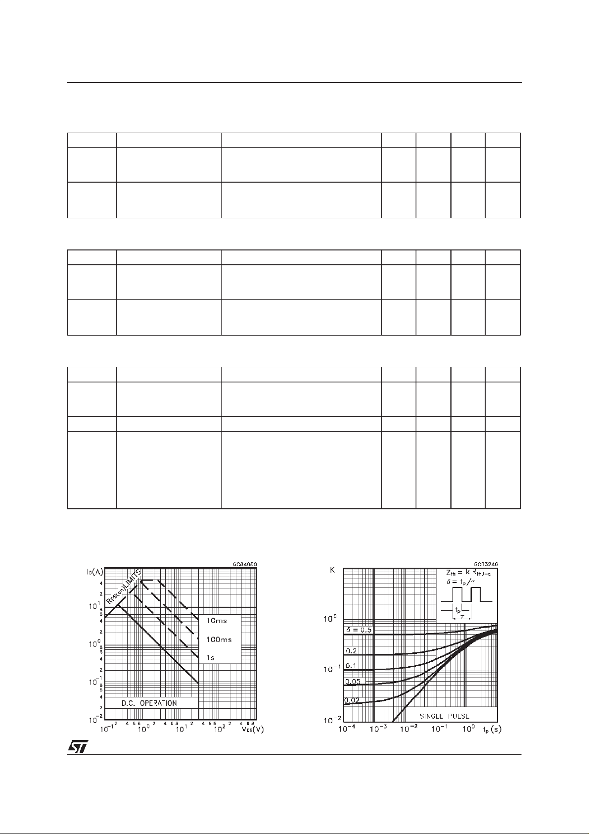
SafeOperating Area ThermalImpedance
3/8
Page 4

STS12NF30L
OutputCharacteristics
Transconductance
TransferCharacteristics
Static Drain-sourceOn Resistance
Gate Charge vs Gate-sourceVoltage
4/8
CapacitanceVariations
Page 5

STS12NF30L
NormalizedGate ThresholdVoltage vs
Temperature
Source-drainDiode Forward Characteristics
NormalizedOn Resistancevs Temperature
5/8
Page 6

STS12NF30L
Fig. 1:
UnclampedInductiveLoad TestCircuit
Fig. 3: SwitchingTimes Test Circuits For
ResistiveLoad
Fig. 2:
UnclampedInductiveWaveform
Fig. 4: Gate Chargetest Circuit
Fig. 5:
Test Circuit For InductiveLoad Switching
And Diode Recovery Times
6/8
Page 7

SO-8 MECHANICAL DATA
STS12NF30L
DIM.
MIN. TYP. MAX. MIN. TYP. MAX.
A 1.75 0.068
a1 0.1 0.25 0.003 0.009
a2 1.65 0.064
a3 0.65 0.85 0.025 0.033
b 0.35 0.48 0.013 0.018
b1 0.19 0.25 0.007 0.010
C 0.25 0.5 0.010 0.019
c1 45 (typ.)
D 4.8 5.0 0.188 0.196
E 5.8 6.2 0.228 0.244
e 1.27 0.050
e3 3.81 0.150
F 3.8 4.0 0.14 0.157
L 0.4 1.27 0.015 0.050
M 0.6 0.023
S 8 (max.)
mm inch
0016023
7/8
Page 8

STS12NF30L
Information furnishedis believed tobeaccurateand reliable.However, STMicroelectronics assumesno responsibilityfor the consequences
of use of such information nor for any infringement of patents or other rights of third parties which may result from its use. No licenseis
granted by implication or otherwise under anypatent or patent rights of STMicroelectronics. Specificationmentioned in this publication are
subjecttochange withoutnotice.Thispublication supersedes and replaces all informationpreviously supplied. STMicroelectronicsproducts
are not authorized for use as critical components in lifesupportdevices or systemswithout express written approval of STMicroelectronics.
The STlogo is a trademark of STMicroelectronics
1999 STMicroelectronics – Printed in Italy – All Rights Reserved
STMicroelectronics GROUP OF COMPANIES
Australia - Brazil - Canada -China - France - Germany - Italy - Japan - Korea - Malaysia - Malta - Mexico - Morocco - The Netherlands -
8/8
Singapore - Spain - Sweden - Switzerland - Taiwan - Thailand - United Kingdom - U.S.A.
http://www.st.com
.
 Loading...