

Page 1
N - CHANNEL 30V - 0.011Ω - 10A SO-8
TYPE V
ST S10NF30L 30 V < 0.0135 Ω 10 A
■ TYPICALR
■ STANDARD OUTLINE FOR EASY
DS(on)
DSS
= 0.011 Ω
AUTOMATEDSURFACEMOUNTASSEMBLY
■ LOW THRESHOLDDRIVE
DESCRIPTION
This Power MOSFET is the secondgeneration of
STMicroelectronics unique ” Single Feature
Size
”
strip-based process. The resulting
transistor shows extremely high packing density
for low on-resistance, rugged avalanche
characteristics and less critical alignment steps
therefore a remarkable manufacturing
reproducibility.
R
DS(on)
I
D
STS10NF30L
STripFET POWER MOSFET
PRELIMINARY DATA
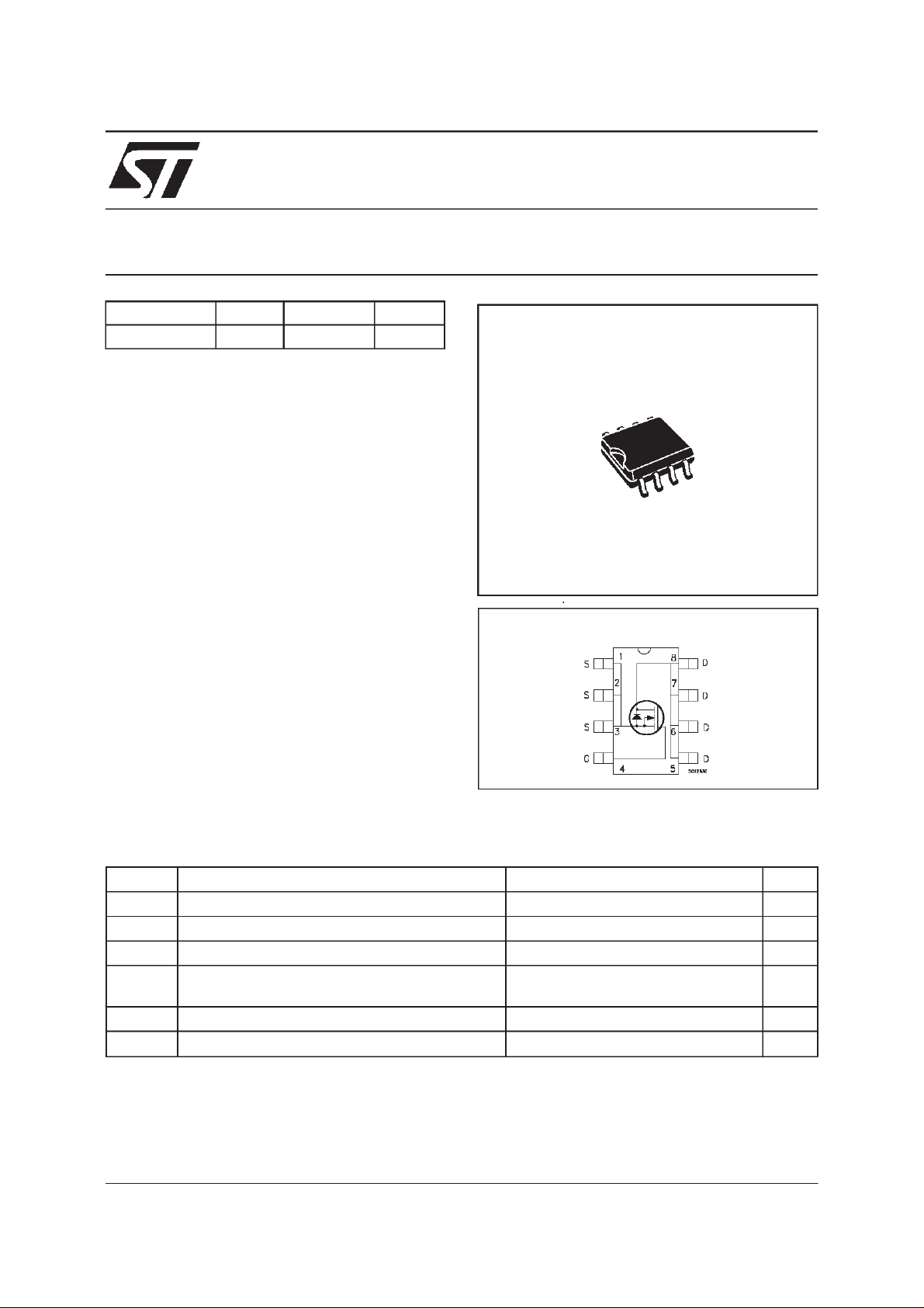
SO-8
APPLICATIONS
■ DC MOTOR DRIVE
■ DC-DCCONVERTERS
■ BATTERYMANAGMENTIN NOMADIC
INTERNAL SCHEMATIC DIAGRAM
EQUIPMENT
■ POWERMANAGEMENTIN
PORTABLE/DESKTOPPC
s
ABSOLUTE MAXIMUM RATINGS
Symb o l Parameter Value Unit
V
V
V
I
DM
P
(•) Pulse width limited by safeoperating area
Drain-source Voltage (VGS=0) 30 V
DS
Drain- g at e Voltage (RGS=20kΩ)30V
DGR
Gate-s ource Voltage ± 20 V
GS
Drain Cur rent (co nt inuous) at T c = 25oC
I
D
Drain Cur rent (co nt inuous) at T
(•) Drain Curr ent (pulsed) 40 A
Tot al Dissi pat ion at Tc = 25oC 2.5 W
tot
=100oC
c
10
6.5
A
A
June 2000
1/6
Page 2
STS10NF30L
THERMAL DATA
R
thj-amb
Tj
T
(*)
Mountedon FR-4board (t
(*)T hermal Resist ance Junction-ambient
Maximum Operating J unct ion Tem p er at ure
stg
St orage Tem pe ra tur e
≤ 10
sec)
50
150
-55 to 150
o
C/W
o
o
C
C
ELECTRICAL CHARACTERISTICS (T
=25oC unless otherwisespecified)
case
OFF
Symbol Parameter Test Conditions Min. Typ. Max. Unit
V
(BR)DSS
Drain-source
ID=250µAVGS=0 30 V
Break dow n Vo lt age
I
I
ON (∗
DSS
GSS
Zero Gate Voltage
Drain Curre nt (V
Gat e- bod y Leakag e
Current (V
)
DS
=0)
GS
=0)
V
=MaxRating
DS
=MaxRating Tc=125oC
V
DS
V
= ± 20 V ± 100 nA
GS
1
10
Symbol Parameter Test Conditions Min. Typ. Max. Unit
V
GS(th)
R
DS(on)
I
D(on)
Gate Threshold Voltage VDS=VGSID= 250 µA11.62.5V
Sta t ic Drain-s our c e On
Resistance
On State Drain Current VDS>I
VGS=10V ID=5A
V
=4.5V ID=5A
GS
D(on)xRDS(on )max
0.011
0.016
0.0135
0.0220
10 A
VGS=10V
DYNAMIC
Symbol Parameter Test Conditions Min. Typ. Max. Unit
g
(∗)Forward
fs
Tr ansc on duc tance
C
C
C
Input Capaci t ance
iss
Out put Capac itance
oss
Reverse Transfer
rss
Capacit a nc e
VDS>I
D(on)xRDS(on )maxID
=5A 20 S
VDS=25V f=1MHz VGS= 0 V 1450
390
150
µA
µ
Ω
Ω
pF
pF
pF
A
2/6
Page 3

STS10NF30L
ELECTRICAL CHARACTERISTICS
(continued)
SWITCHINGON
Symbol Parameter Test Conditions Min. Typ. Max. Unit
t
d(on)
Tur n-on Delay T ime
Rise Time
t
r
VDD=15V ID=5A
R
=4.7
G
Ω
VGS=4.5V
25
280
(Resis t iv e Load, see fig. 3)
Q
Q
Q
Tot al Gate Charge
g
Gat e- Source Charge
gs
Gate-Drain Charge
gd
VDD=24V ID=10A VGS=10V 25
11
12
35 nC
SWITCHINGOFF
Symbol Parameter Test Conditions Min. Typ. Max. Unit
t
d(off)
Tur n-of f Dela y Tim e
t
Fall T ime
f
VDD=15V ID=5A
=4.7 Ω VGS=4.5V
R
G
40
60
(Resis t iv e Load, see fig. 3)
SOURCEDRAINDIODE
Symbol Parameter Test Conditions Min. Typ. Max. Unit
I
SD
I
SDM
V
SD
t
Q
I
RRM
(∗) Pulsed: Pulse duration = 300 µs, duty cycle 1.5 %
(•) Pulse width limited by safe operatingarea
Source-drain Current
(•)
Source-drain Current
10
40
(pulsed)
(∗)ForwardOnVoltage ISD=10A VGS=0 1.2 V
Reverse Recovery
rr
Time
Reverse Recovery
rr
ISD= 10 A di/dt = 100 A/µs
=15V Tj=150oC
V
DD
(see test circuit, fig. 5)
45
52
Charge
Reverse Recovery
2.3
Current
ns
ns
nC
nC
ns
ns
A
A
ns
nC
A
3/6
Page 4

STS10NF30L
Fig. 1:
UnclampedInductiveLoad TestCircuit
Fig. 3: SwitchingTimes Test Circuits For
ResistiveLoad
Fig. 2:
UnclampedInductiveWaveform
Fig. 4: Gate Chargetest Circuit
Fig. 5:
Test CircuitFor InductiveLoad Switching
And Diode Recovery Times
4/6
Page 5

SO-8 MECHANICALDATA
STS10NF30L
DIM.
MIN. TYP. MAX. MIN. TYP. MAX.
A 1.75 0.068
a1 0.1 0.25 0.003 0.009
a2 1.65 0.064
a3 0.65 0.85 0.025 0.033
b 0.35 0.48 0.013 0.018
b1 0.19 0.25 0.007 0.010
C 0.25 0.5 0.010 0.019
c1 45 (typ.)
D 4.8 5.0 0.188 0.196
E 5.8 6.2 0.228 0.244
e 1.27 0.050
e3 3.81 0.150
F 3.8 4.0 0.14 0.157
L 0.4 1.27 0.015 0.050
M 0.6 0.023
S 8 (max.)
mm inch
0016023
5/6
Page 6

STS10NF30L
Information furnished is believed to be accurate and reliable. However, STMicroelectronics assumes no responsibility for the consequences
of use of such information nor for any infringement of patents or other rights of third parties which may result from its use. No license is
granted by implicationor otherwise under any patent or patent rights of STMicroelectronics. Specification mentioned in thispublication are
subject to change without notice. This publication supersedes and replaces all information previously supplied. STMicroelectronics products
are not authorized for use as critical components in life support devices or systems without express written approval of STMicroelectronics.
The ST logo is a trademarkof STMicroelectronics
2000 STMicroelectronics – Printed in Italy – All Rights Reserved
STMicroelectronics GROUP OF COMPANIES
Australia - Brazil -China - Finland - France - Germany - Hong Kong - India - Italy - Japan - Malaysia - Malta - Morocco -
Singapore - Spain - Sweden -Switzerland - United Kingdom - U.S.A.
http://www.st.com
6/6
 Loading...