

Page 1
ARM7TDMI™ 32-bit MCU with Flash, 3x CAN,
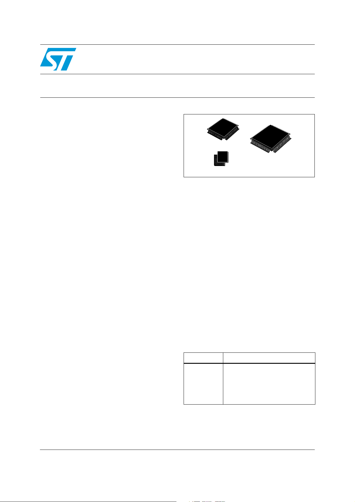
TQFP144
20 x 20
TQFP100 14 x 14
LFBGA144 10 x 10 x 1.7
4 UARTs, 20 timers, ADC, 12 comm. interfaces
Features
■ Core
– ARM7TDMI 32-bit RISC CPU
– 32 MIPS @ 36 MHz
■ Memories
– Up to 256 Kbytes Flash program memory
(10,000 cycles endurance, data retention
20 years @ 85° C)
– 16 Kbytes RAM
■ Clock, reset and supply management
– 4.5 - 5.5 V application supply and I/Os
– Embedded 1.8 V regulator for core supply
– Embedded oscillator running from external
4-8 MHz crystal or ceramic resonator
– Up to 36 MHz CPU frequency with internal
PLL
– 32 kHz or 2 MHz internal RC oscillator,
software configurable for fast startup and
backup clock
– Real-time clock for clock-calendar function
– Wake-up timer driven by internal RC for
wake-up from STOP mode
– 5 power saving modes: SLOW, WFI,
LPWFI, STOP and HALT modes
■ Nested interrupt controller
– Fast interrupt handling with multiple vectors
– 64 maskable IRQs with 64 vectors and 16
priority levels
– 2 maskable FIQ sources
– 16 external interrupts, up to 32 wake-up
lines
■ Up to 112 I/O ports
– 72/112 multifunctional bidirectional I/Os
STR73xFxx
■ DMA
– 4 DMA controllers with 4 channels each
■ Timers
– 16-bit watchdog timer (WDG)
– 6/10 16-bit timers (TIM) each with: 2 input
captures, 2 output compares, PWM and
pulse counter modes
– 6 16-bit PWM modules (PWM)
– 3 16-bit timebase timers with 8-bit
prescalers
■ 12 communications interfaces
2
–2 I
C interfaces
– 4 UART asynchronous serial interfaces
– 3 BSPI synchronous serial interfaces
–Up to 3 CAN interfaces (2.0B Active)
■ 10-bit A/D converter
– 12/16 channels
– Conversion time: min. 3 µs, range: 0 to 5V
■ Development tools support
–JTAG interface
Table 1. Device summary
Reference Part number
STR730FZ1, STR730FZ2,
STR731FV0, STR731FV1,
STR73xFxx
STR731FV2,
STR735FZ1, STR735FZ2,
STR736FV0, STR736FV1,
STR736FV2
June 2008 Rev 7 1/52
www.st.com
52
Page 2

Contents STR73xFxx
Contents
1 Scope . . . . . . . . . . . . . . . . . . . . . . . . . . . . . . . . . . . . . . . . . . . . . . . . . . . . . 4
1.1 Description . . . . . . . . . . . . . . . . . . . . . . . . . . . . . . . . . . . . . . . . . . . . . . . . . 4
2 Overview . . . . . . . . . . . . . . . . . . . . . . . . . . . . . . . . . . . . . . . . . . . . . . . . . . 5
2.1 On-chip peripherals . . . . . . . . . . . . . . . . . . . . . . . . . . . . . . . . . . . . . . . . . . 6
3 Block diagram . . . . . . . . . . . . . . . . . . . . . . . . . . . . . . . . . . . . . . . . . . . . . . 8
3.1 Related documentation . . . . . . . . . . . . . . . . . . . . . . . . . . . . . . . . . . . . . . 10
3.2 Pin description . . . . . . . . . . . . . . . . . . . . . . . . . . . . . . . . . . . . . . . . . . . . . 11
3.2.1 STR730F/STR735F (TQFP144) . . . . . . . . . . . . . . . . . . . . . . . . . . . . . . 11
3.2.2 STR730F/STR735F (LFBGA144) . . . . . . . . . . . . . . . . . . . . . . . . . . . . . 12
3.2.3 STR731F/STR736F (TQFP100) . . . . . . . . . . . . . . . . . . . . . . . . . . . . . . 13
3.3 Memory mapping . . . . . . . . . . . . . . . . . . . . . . . . . . . . . . . . . . . . . . . . . . . 20
4 Electrical parameters . . . . . . . . . . . . . . . . . . . . . . . . . . . . . . . . . . . . . . . 21
4.1 Parameter conditions . . . . . . . . . . . . . . . . . . . . . . . . . . . . . . . . . . . . . . . . 21
4.1.1 Minimum and maximum values . . . . . . . . . . . . . . . . . . . . . . . . . . . . . . . 21
4.1.2 Typical values . . . . . . . . . . . . . . . . . . . . . . . . . . . . . . . . . . . . . . . . . . . . . 21
4.1.3 Typical curves . . . . . . . . . . . . . . . . . . . . . . . . . . . . . . . . . . . . . . . . . . . . 21
4.1.4 Loading capacitor . . . . . . . . . . . . . . . . . . . . . . . . . . . . . . . . . . . . . . . . . 21
4.1.5 Pin input voltage . . . . . . . . . . . . . . . . . . . . . . . . . . . . . . . . . . . . . . . . . . 21
4.2 Absolute maximum ratings . . . . . . . . . . . . . . . . . . . . . . . . . . . . . . . . . . . . 22
4.3 Operating conditions . . . . . . . . . . . . . . . . . . . . . . . . . . . . . . . . . . . . . . . . 24
4.3.1 Supply current characteristics . . . . . . . . . . . . . . . . . . . . . . . . . . . . . . . . 25
4.3.2 Clock and timing characteristics . . . . . . . . . . . . . . . . . . . . . . . . . . . . . . 29
4.3.3 Memory characteristics . . . . . . . . . . . . . . . . . . . . . . . . . . . . . . . . . . . . . 34
4.3.4 EMC characteristics . . . . . . . . . . . . . . . . . . . . . . . . . . . . . . . . . . . . . . . . 35
4.3.5 I/O port pin characteristics . . . . . . . . . . . . . . . . . . . . . . . . . . . . . . . . . . . 38
4.3.6 10-bit ADC characteristics . . . . . . . . . . . . . . . . . . . . . . . . . . . . . . . . . . . 43
5 Package characteristics . . . . . . . . . . . . . . . . . . . . . . . . . . . . . . . . . . . . . 46
5.1 Package mechanical data . . . . . . . . . . . . . . . . . . . . . . . . . . . . . . . . . . . . 46
5.2 Thermal characteristics . . . . . . . . . . . . . . . . . . . . . . . . . . . . . . . . . . . . . . 48
2/52
Page 3

STR73xFxx Contents
6 Order codes . . . . . . . . . . . . . . . . . . . . . . . . . . . . . . . . . . . . . . . . . . . . . . . 49
7 Known limitations . . . . . . . . . . . . . . . . . . . . . . . . . . . . . . . . . . . . . . . . . . 50
7.1 Low power wait for interrupt mode . . . . . . . . . . . . . . . . . . . . . . . . . . . . . . 50
7.2 PLL free running mode at high temperature . . . . . . . . . . . . . . . . . . . . . . 50
8 Revision history . . . . . . . . . . . . . . . . . . . . . . . . . . . . . . . . . . . . . . . . . . . 51
3/52
Page 4

Scope STR73xFxx
1 Scope
This datasheet provides the STR73x ordering information, mechanical and electrical device
characteristics.
For complete information on the STR73xF microcontroller memory, registers and
peripherals. please refer to the STR73x reference manual.
For information on programming, erasing and protection of the internal Flash memory
please refer to the STR7 Flash programming reference manual.
For information on the ARM7TDMI core please refer to the ARM7TDMI technical reference
manual.
1.1 Description
ARM core with embedded Flash & RAM
STR73xF family combines the high performance ARM7TDMI
of peripheral functions and enhanced I/O capabilities. All devices have on-chip high-speed
single voltage Flash memory and high-speed RAM. The STR73xF family has an embedded
ARM core and is therefore compatible with all ARM tools and software.
™
CPU with an extensive range
Extensive tools support
STMicroelectronics’ 32-bit, ARM core-based microcontrollers are supported by a complete
range of high-end and low-cost development tools to meet the needs of application
developers. This extensive line of hardware/software tools includes starter kits and complete
development packages all tailored for ST’s ARM core-based MCUs.
The range of development packages includes third-party solutions that come complete with
a graphical development environment and an in-circuit emulator/programmer featuring a
JTAG application interface. These support a range of embedded operating systems (OS),
while several royalty-free OSs are also available.
For more information, please refer to ST MCU site http://www.st.com/mcu
Figure 1 shows the general block diagram of the device family.
4/52
Page 5
STR73xFxx Overview
2 Overview
Table 2. Product overview
Flash memory - bytes 128K 256K 128K 256K 64K 128K 256K 64K 128K 256K
Peripheral functions
CAN peripherals 3 0 3 0
Operating voltage 4.5 to 5.5 V
Operating temperature -40 to +85°C/-40 to +105° C
Features STR730FZx STR735FZx STR731FVx STR736FVx
RAM - bytes 16 K 16 K
Packages
10 TIM timers, 112 I/Os,
32 wake-up lines, 16 ADC
T=TQFP144 20 x 20
H=LFBGA144 10 x10
6 TIM timers, 72 I/Os, 18 wake-up lines,
12 ADC channels
T=TQFP100 14x14
Package choice: reduced pin-count TQFP100 or feature-rich 144-pin TQFP or LFBGA
The STR73xF family is available in 3 packages. The TQFP144 and LFBGA144 versions
have the full set of all features. The 100-pin version has fewer timers, I/Os and ADC
channels. Refer to the Device Summary on Page 1 for a comparison of the I/Os available on
each package.
The family includes versions with and without CAN.
High speed Flash memory
The Flash program memory is organized in 32-bit wide memory cells which can be used for
storing both code and data constants. It is accessed by CPU with zero wait states @ 36
MHz.
The STR7 embedded Flash memory can be programmed using in-circuit programming or
in-application programming.
The Flash memory endurance is 10K write/erase cycles and the data retention is 20 years
@ 85° C.
IAP (in-application programming): IAP is the ability to re-program the Flash memory of a
microcontroller while the user program is running.
ICP (in-circuit programming): ICP is the ability to program the Flash memory of a
microcontroller using JTAG protocol while the device is mounted on the user application
board.
The Flash memory can be protected against different types of unwanted access
(read/write/erase). There are two types of protection:
● Sector write protection
● Flash debug protection (locks JTAG access)
Flexible power management
To minimize power consumption, you can program the STR73xF to switch to SLOW, WFI
LPWFI, STOP or HALT modes depending on the current system activity in the application.
5/52
Page 6

Overview STR73xFxx
Flexible clock control
Two clock sources are used to drive the microcontroller, a main clock driven by an external
crystal or ceramic resonator and an internal backup RC oscillator that operates at 2 MHz or
32 kHz. The embedded PLL can be configured to generate an internal system clock of up to
36 MHz. The PLL output frequency can be programmed using a wide selection of multipliers
and dividers.
Voltage regulators
The STR73xF requires an external 4.5 to 5.5 V power supply. There are two internal Voltage
Regulators for generating the 1.8 V power supply needed by the core and peripherals. The
main VR is switched off and the Low Power VR switched on when the application puts the
STR73xF in Low Power Wait for Interrupt (LPWFI) mode.
Low voltage detectors
The voltage regulator and Flash modules each have an embedded LVD that monitors the
internal 1.8 V supply. If the voltage drops below a certain threshold, the LVD will reset the
STR73xF.
Note: An external power-on reset must be provided ensure the microcontroller starts-up correctly.
2.1 On-chip peripherals
CAN interfaces
The three CAN modules are compliant with the CAN specification V2.0 part B (active). The
bit rate can be programmed up to 1 MBaud. These are not available in the STR735 and
STR736.
DMA
4 DMA controllers, each with 4 data streams manage memory to memory, peripheral to
peripheral, peripheral to memory and memory to peripheral transfers. The DMA requests
are connected to TIM timers, BSPI0, BSPI1, BSPI2 and ADC. One of the streams can be
configured to be triggered by a software request, independently from any peripheral activity.
16-bit timers (TIM)
Each of the ten timers (six in 100-pin devices) have a 16-bit free-running counter with 7-bit
prescaler, up to two input capture/output compare functions, a pulse counter function, and a
PWM channel with selectable frequency. This provides a total of 16 independent PWMs (12
in 100-pin devices) when added with the PWM modules (see next paragraph).
PWM modules (PWM)
The six 16-bit PWM modules have independently programmable periods and duty-cycles,
with 5+3 bit prescaler factor.
Timebase timers (TB)
The three 16-bit timebase timers with 8-bit prescaler for general purpose time triggering
operations.
Real-time clock (RTC)
The RTC provides a set of continuously running counters driven by separate clock signal
derived from the main oscillator. The RTC can be used as a general timebase or
6/52
Page 7

STR73xFxx Overview
clock/calendar/alarm function. When the STR73xF is in LPWFI mode the RTC keeps
running, powered by the low power voltage regulator.
UARTs
The 4 UARTs allow full duplex, asynchronous, communications with external devices with
independently programmable TX and RX baud rates up to 625 Kbaud.
Buffered serial peripheral interfaces (BSPI)
Each of the three BSPIs allow full duplex, synchronous communications with external
devices, master or slave communication at up to 6 Mb/s in master mode and up to 4.5 Mb/s
in slave mode (@36 MHz system clock).
2
I
C interfaces
The two I
2
I
C mode (400 kHz) and 7 or 10-bit addressing modes.
2
C Interfaces provide multi-master and slave functions, support normal and fast
A/D converter
The 10-bit analog to digital converter, converts up to 16 channels in single-shot or
continuous conversion modes (12 channels in 100-pin devices). The minimum conversion
time is 3 µs.
Watchdog
The 16-bit watchdog timer protects the application against hardware or software failures and
ensures recovery by generating a reset.
I/O ports
Up to 112 I/O ports (72 in 100-pin devices) are programmable as general purpose
input/output or alternate function.
External interrupts and wake-up lines
16 external interrupts lines are available for application use. In addition, up to 32 external
Wake-up lines (18 in 100-pin devices) can be used as general purpose interrupts or to
wake-up the application from STOP mode.
7/52
Page 8
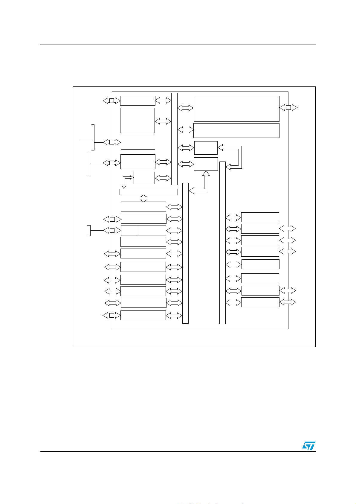
Block diagram STR73xFxx
APB BUS
122 ports
GPIO PORTS 0-6
WATCHDOG
I2C0-1
WAKE-UP/INT (WIU)
UART0, 1, 2, 3
WAKE-UP TIMER
APB BUS
BSPI 0-2
RTC
CAN 0-2*
INTERRUPT CTL (EIC)
A/D CONVERTER (ADC)
32 AF
8 AF
16 AF
12 AF
XTAL1
XTAL2
OSC
TIMER (TIM) 2-4
4 AF
AF: alternate function on I/O port pin
PWM 0-5
CLOCK MGT (CMU)
TIMER (TIM) 0-1
8 AF
TIMER (TIM) 5-9
20 AF
6 AF
(WUT)
TIMEBASE TIMER
(TB) 0-2
6 AF
12 AF
*CAN peripherals not available on STR735F.
FLASH
PROGRAM MEMORY
64/128/256K
APB
BRIDGE 0
APB
BRIDGE 1
POWER SUPPLY
PRCCU/PLL
RAM
16K
JTAG
ARM7TDMI
CPU
JTDI
JTCK
JTMS
JTRST
JTDO
RSTIN
V18
VDD
VSS
VREG
VDDA
VSSA
ARM7 NATIVE BUS
DMA0-3
AHB BUS
AHB
BRIDGE
M0
M1
TEST
3 Block diagram
Figure 1. STR730F/STR735F block diagram
8/52
Page 9
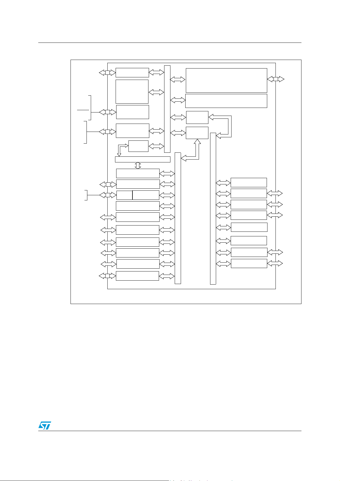
STR73xFxx Block diagram
APB BUS
72 ports
GPIO PORTS 0-6
FLASH
PROGRAM MEMORY
64/128/256K
WATCHDOG
I2C0-1
WAKE-UP/INT (WIU)
UART0, 1, 2, 3
WAKE-UP TIMER
APB
BRIDGE 0
APB
BRIDGE 1
APB BUS
BSPI 0-2
RTC
CAN 0-2*
INTERRUPT CTL (EIC)
A/D CONVERTER (ADC)
POWER SUPPLY
PRCCU/PLL
RAM
16K
JTAG
ARM7TDMI
CPU
18 AF
8 AF
12 AF
12 AF
XTAL1
XTAL2
JTDI
JTCK
JTMS
JTRST
JTDO
RSTIN
V18
VDD
VSS
OSC
VREG
VDDA
VSSA
TIMER (TIM) 2-4
ARM7 NATIVE BUS
4 AF
AF: alternate function on I/O port pin
PWM 0-5
CLOCK MGT (CMU)
DMA0-3
TIMER (TIM) 0-1
8 AF
TIMER (TIM) 5
4 AF
6 AF
(WUT)
TIMEBASE TIMER
(TB) 0-2
AHB BUS
AHB
BRIDGE
6 AF
M0
M1
TEST
12 AF
*CAN peripherals not available on STR736F.
Figure 2. STR731F/STR736 block diagram
9/52
Page 10

Block diagram STR73xFxx
3.1 Related documentation
Available from www.arm.com:
ARM7TDMI technical reference manual
Available from http://www.st.com:
STR73x reference manual (RM0001)
STR7 Flash programming reference manual
STR73x software library user manual
For a list of related application notes refer to http://www.st.com.
10/52
Page 11
STR73xFxx Block diagram
1
2
3
4
5
6
7
8
9
10
11
12
13
14
15
16
17
18
19
20
21
22
23
24
25
26
27
28
29
30
31
32
33
34
35
36
108
107
106
105
104
103
102
101
100
99
98
97
96
95
94
93
92
91
90
89
88
87
86
85
84
83
82
81
80
79
78
77
76
75
74
73
3738394041424344454647484950515253545556575859606162636465666768697071
72
144
143
142
141
140
139
138
137
136
135
134
133
132
131
130
129
128
127
126
125
124
123
122
121
120
119
118
117
116
115
114
113
112
111
110
109
OCMPB2 / P0.0
OCMPA2 / P0.1
ICAPA2 / P0.2
ICAPB2 / P0.3
V
SS
V
DD
OCMPA5 / P0.4
OCMPB5 / P0.5
ICAPA5 / P0.6
ICAPB5 / P0.7
OCMPA6 / P0.8
OCMPB6 / P0.9
OCMPA7 / P0.10
OCMPB7 / P0.11
V
DD
V
SS
ICAPA3 / P0.12
ICAPB3 / P0.13
OCMPB3 / P0.14
OCMPA3 / P0.15
OCMPA4 / P1.0
OCMPB4 / P1.1
ICAPB4 / P1.2
ICAPA4 / P1.3
V
SS
V
DD
P1.4
P1.5
OCMPB1 / P1.6
OCMPA1 / P1.7
INT0 / OCMPA0 / P1.8
INT1 / OCMPB0 / P1.9
ICAPB0 / WUP28 / P1.10
ICAPA0 / WUP29 / P1.11
ICAPA1 / WUP30 / P1.12
ICAPB1 / WUP31 / P1.13
P4.14 / SS1
P4.13 / ICAPB9
P4.12 / ICAPA9 / WUP21
P4.11 / OCMPB8
P4.10 / ICAPA6 / WUP20
P4.9 / ICAPB6
P4.8 / OCMPA8
P4.7 / SDA1
P4.6 / SCL1 / WUP19
P4.5 / CAN2RX / WUP18
P4.4 / CAN2TX
P4.3 / ICAPB8 / WUP27
P4.2 / ICAPA8 / WUP26
P4.1 / ICAPB7 / WUP25
P4.0 / ICAPA7 / WUP24
V
DD
V
SS
JTDO
JTCK
JTMS
JTDI
JTRST
V
SS
V
DD
P3.15 / AIN15 / INT5
P3.14 / AIN14 / INT4
P3.13 / AIN13 / INT3
P3.12 / AIN12 / INT2
P3.11 / AIN11
P3.10 / AIN10
P3.9 / AIN9
P3.8 / AIN8
V
DDA
V
SSA
P3.7 / AIN7
P3.6 / AIN6
WUP12 / CAN0RX / P1.14
CAN0TX / P1.15
PWM0 / P2.0
WUP13 / CAN1RX / P2.1
CAN1TX / P2.2
PWM1 / P2.3
PWM2 / P2.4
PWM3 / P2.5
PWM4 / P2.6
PWM5 / P2.7
M0
RSTIN
M1
V
DD
V
SS
XTAL1
XTAL2
V
SS
TDO1 / P2.8
WUP14 / RDI1 / P2.9
WUP16 / P2.10
WUP17 / P2.11
INT14 / P2.12
INT15 / P2.13
WUP15 / SCL0 / P2.14
SDA0 / P2.15
TEST
V
BIAS
V
SS
V
DD
AIN0 / P3.0
AIN1 / P3.1
AIN2 / P3.2
AIN3 / P3.3
AIN4 / P3.4
AIN5 / P3.5
P6.15 / WUP9
P6.14 / SS0
P6.13 / SCK0 / WUP11
P6.12 / MOSI0
P6.11 / MISO0
P6.10 / WUP8
P6.9 / TDO0
P6.8 / RDI0 / WUP10
P6.7 / WUP7
P6.6 / WUP6
P6.5 / WUP5
P6.4 / TDO3 / WUP4
P6.3 / WUP3
P6.2 / RDI3 / WUP2
P6.1 / WUP1
P6.0 / WUP0
VDD
VSS
V18
P5.15 / INT13
P5.14 / INT12
P5.13 / INT11
P5.12 / INT10
P5.11 / TDO2 / INT9
P5.10 / RDI2 / INT8
P5.9 / INT7
P5.8 / INT6
P5.7 / MISO2
P5.6 / MOSI2
P5.5 / SCK2 / WUP23
P5.4 / SS2
P5.3 / OCMPB9
P5.2 / OCMPA9
P5.1 / MISO1
P5.0 / MOSI1
P4.15 / SCK1 / WUP22
STR730F/STR735F
Note: CAN alternate functions not available on STR735F.
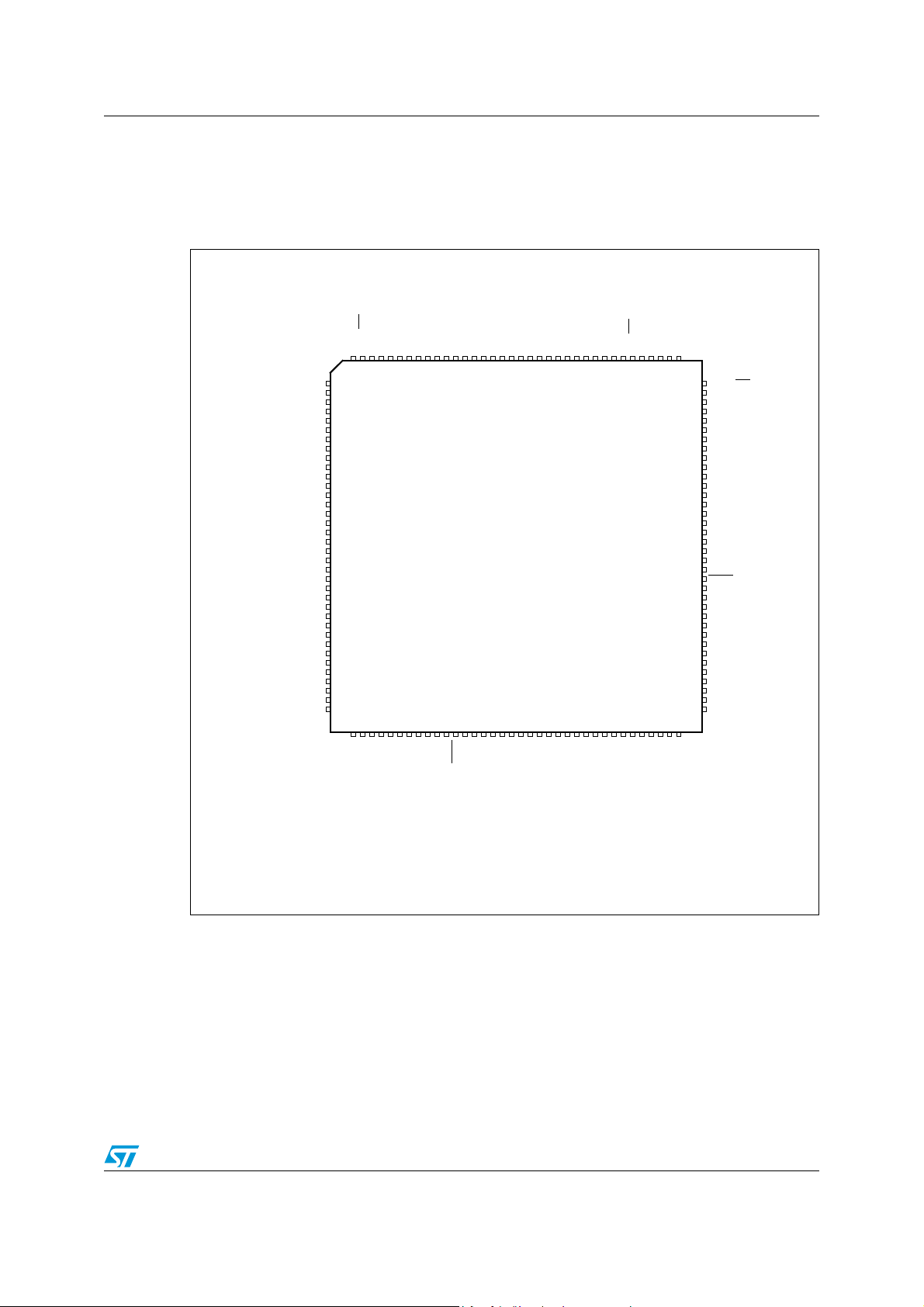
3.2 Pin description
3.2.1 STR730F/STR735F (TQFP144)
Figure 3. STR730F/STR735F pin configuration (top view)
11/52
Page 12
Block diagram STR73xFxx
3.2.2 STR730F/STR735F (LFBGA144)
Table 3. STR730F/STR735F LFBGA ball connections
Ball Name Ball Name Ball Name Ball Name
A1 P0.0 / OCMPB2 B1 P0.4 / OCMPA5 C1 P0.5 / OCMPB5 D1 V
A2 P6.10 / WUP8 B2 P0.1 / OCMPA2 C2 P0.2 / ICAPA2 D2 V
A3 P6.9 / TDO0 B3 P6.15 / WUP9 C3 P0.3 / ICAPB2 D3 P0.6 / ICAPA5
A4 P6.12 / MOSI0 B4 P6.13 / SCKO / WUP11 C4 P6.14 / SSO D4 P0.7 /ICAPB5
A5 P6.6 / WUP6 B5 P6.7 / WUP7 C5 P6.8 / RDI0 / WUP10 D5 P6.11 / MISO0
A6 V
18
A7 P5.15 / INT13 B7 P5.14 / INT12 C7 V
B6 P6.2 / WUP2 / RDI3 C6 P6.3 / WUP3 D6 P6.4 / WUP4 /TDO3
SS
D7 VDD
A8 P5.8 / INT6 B8 P5.9 / INT7 C8 P5.10 / INT8 / RDI2 D8 P5.12 / INT10
A9 P5.2 / OCMPA9 B9 P5.3 / OCMPB9 C9 P5.4 / SS2 D9 P5.5 / SCK2 / WUP23
A10 P5.7 / MISO2 B10 P5.0 / MOSI1 C10 P5.1 / MISO1 D10 P4.13 / ICAPB9
A11 P5.6 / MOSI2 B11 P4.15 / SCK1 / WUP22 C11 P4.14 / SS1 D11 P4.12 / ICAPA9 / WUP21
A12 P5.11 / TDO2 / INT9 B12 P4.8 / OCMPA8 C12 P4.7 / SDA1 D12 P4.11 / OCMPB8
E1 P0.8 / OCMPA6 F1 V
DD
G1 V
SS
H1 V
E2 P0.9 / OCMPB6 F2 P0.13 / ICAPB3 G2 P1.2 / ICAPB4 H2 P1.8 / OCMPA0 / INT0
E3 P0.10 / OCMPA7 F3 P0.14 / OCMPB3 G3 P1.3 / ICAPA4 H3 P1.9 / OCMPB0 / INT1
E4 P0.11 / OCMPB7 F4 P0.15 / OCMPA3 G4 V
SS
H4 P1.10 / ICAPB0 / WUP28
E5 P0.12 / ICAPA3 F5 P1.0 / OCMPA4 G5 P1.5 H5 XTAL2
E6 P6.5 / WUP5 F6 P1.1 / OCMPB4 G6 P2.11 / WUP17 H6 P2.10 / WUP16
E7 P6.0 / WUP0 F7 P6.1 / WUP1 G7
E8 P5.13 / INT11 F8 P4.4 / CAN2TX
E9
P4.10 / ICAPA6 /
WUP20
F9
E10 P4.9 / ICAPB6 F10
E11 P4.6 / SCL1 / WUP19 F11
E12
P4.5 / WUP18 /
CAN2RX
1)
F12 JTDI G12 nJTRST H12 P3.14 / AIN14 / INT4
P4.3 / ICAPB8 /
WUP27
P4.2 / ICAPA8 /
WUP26
P4.1 / ICAPB7 /
WUP25
1)
G10 JTDO H10 VDD
G11 JTCK H11 P3.15 / AIN15 / INT5
G8 VDD H8 JTMS
G9 VSS H9 VSS
P4.0 / ICAPA7 /
WUP24
J1 P1.4 K1 P1.6 / OCMPB1 L1 P1.7 / OCMPA1 M1
J2
J3
P1.11 / ICAPA0 /
WUP29
P1.12 / ICAPA1 /
WUP30
K2
K3
P1.13 / ICAPB1 /
WUP31
P2.1 / CAN1RX
WUP13
L2 P1.15 / CAN0TX
1)
/
L3 P2.0 / PWM0 M3 P2.5 / PWM3
H7 P2.15 / SDA 0
P1.14 / CAN0RX
1)
M2 P2.4 / PWM2
J4 P2.7 / PWM5 K4 P2.6 / PWM4 L4 P2.3 / PWM1 M4 P2.2 / CAN1TX
J5 V
DD
J6 P2.9 / RDI1 / WUP14 K6 P2.8 / TDO1 L6 V
K5 M1 L5 RSTIN M5 M0
SS
M6 V
J7 P2.14 / SCL 0 / WUP15 K7 P2.13 / INT15 L7 P2.12 / INT14 M7 XTAL1
J8 P3.1 / AIN1 K8 P3.0 / AIN0 L8 VBIAS M8 TST
J9 P3.13 / AIN13 / INT3 K9 P3.4 / AIN4 L9 P3.3 / AIN3 M9 P3.2 / AIN2
J10 P3.12 / AIN12 / INT2 K10 V
J11 P3.9 / AIN9 K11 V
DDA
SSA
L10 P3.5 / AIN5 M10 V
L11 P3.7 / AIN7 M11 V
J12 P3.8 / AIN8 K12 P3.11 / AIN11 L12 P3.10 / AIN10 M12 P3.6 / AIN6
SS
DD
DD
WUP12
SS
SS
DD
1)
/
1)
Note: CAN alternate functions not available on STR735F.
12/52
Page 13
STR73xFxx Block diagram
1
2
3
4
5
6
7
8
9
10
11
12
13
14
15
16
17
18
19
20
21
22
23
24
25
75
74
73
72
71
70
69
68
67
66
65
64
63
62
61
60
59
58
57
56
55
54
53
52
51
26272829303132333435363738394041424344454647484950
100999897969594939291908988878685848382818079787776
OCMPB2 / P0.0
OCMPA2 / P0.1
ICAPA2 / P0.2
ICAPB2 / P0.3
OCMPA5 / P0.4
OCMPB5 / P0.5
ICAPA5 / P0.6
V
DD
V
SS
ICAPA3 / P0.12
ICAPB3 / P0.13
OCMPB3 / P0.14
OCMPA3 / P0.15
OCMPA4 / P1.0
OCMPB4 / P1.1
ICAPB4 / P1.2
ICAPA4 / P1.3
OCMPB1 / P1.6
OCMPA1 / P1.7
INT0 / OCMPA0 / P1.8
INT1 / OCMPB0 / P1.9
ICAPB0 / WUP28 / P1.10
ICAPA0 / WUP29 / P1.11
ICAPA1 / WUP30 / P1.12
ICAPB1 / WUP31 / P1.13
P4.14 / SS1
P4.10 / ICAPB5 / WUP20
P4.7 / SDA1
P4.6 / SCL1 / WUP19
V
DD
V
SS
JTDO
JTCK
JTMS
JTDI
JTRST
V
SS
V
DD
P3.15 / AIN11 / INT5
P3.14 / AIN10 / INT4
P3.13 / AIN9 / INT3
P3.12 / AIN8 / INT2
P3.11 / AIN7
P3.10 / AIN6
P3.9 / AIN5
P3.8 / AIN4
V
DDA
V
SSA
P3.7 / AIN3
P3.6 / AIN2
WUP12 / CAN0RX / P1.14
CAN0TX / P1.15
PWM0 / P2.0
WUP13 / CAN1RX / P2.1
CAN1TX / P2.2
PWM1 / P2.3
PWM2 / P2.4
M0
RSTIN
M1
V
DD
V
SS
XTAL1
XTAL2
V
SS
CAN2RX / TDO1 / P2.8
WUP14 / CAN2TX / RDI1 / P2.9
WUP15 / SCL0 / P2.14
SDA0 / P2.15
TEST
V
BIAS
V
SS
V
DD
AIN0 / P3.4
AIN1 / P3.5
P6.14 / SS0
P6.13 / SCK0 / WUP11
P6.12 / MOSI0
P6.11 / MISO0
P6.9 / TDO0
P6.8 / RDI0 / WUP10
P6.6 / WUP6
P6.4 / TDO3 / WUP4
P6.2 / RDI3 / WUP2
P6.0 / WUP0
VDD
VSS
V18
P5.12 / INT10
P5.11 / TDO2 / INT9
P5.10 / RDI2 / INT8
P5.9 / PWM5 / INT7
P5.8 / PWM4 / INT6
P5.7 / MISO2
P5.6 / MOSI2
P5.5 / SCK2 / WUP23
P5.4 / SS2
/PWM3
P5.1 / MISO1
P5.0 / MOSI1
P4.15 / SCK1 / WUP22
STR731F/STR736F
Note: CAN alternate functions not available on STR736F.
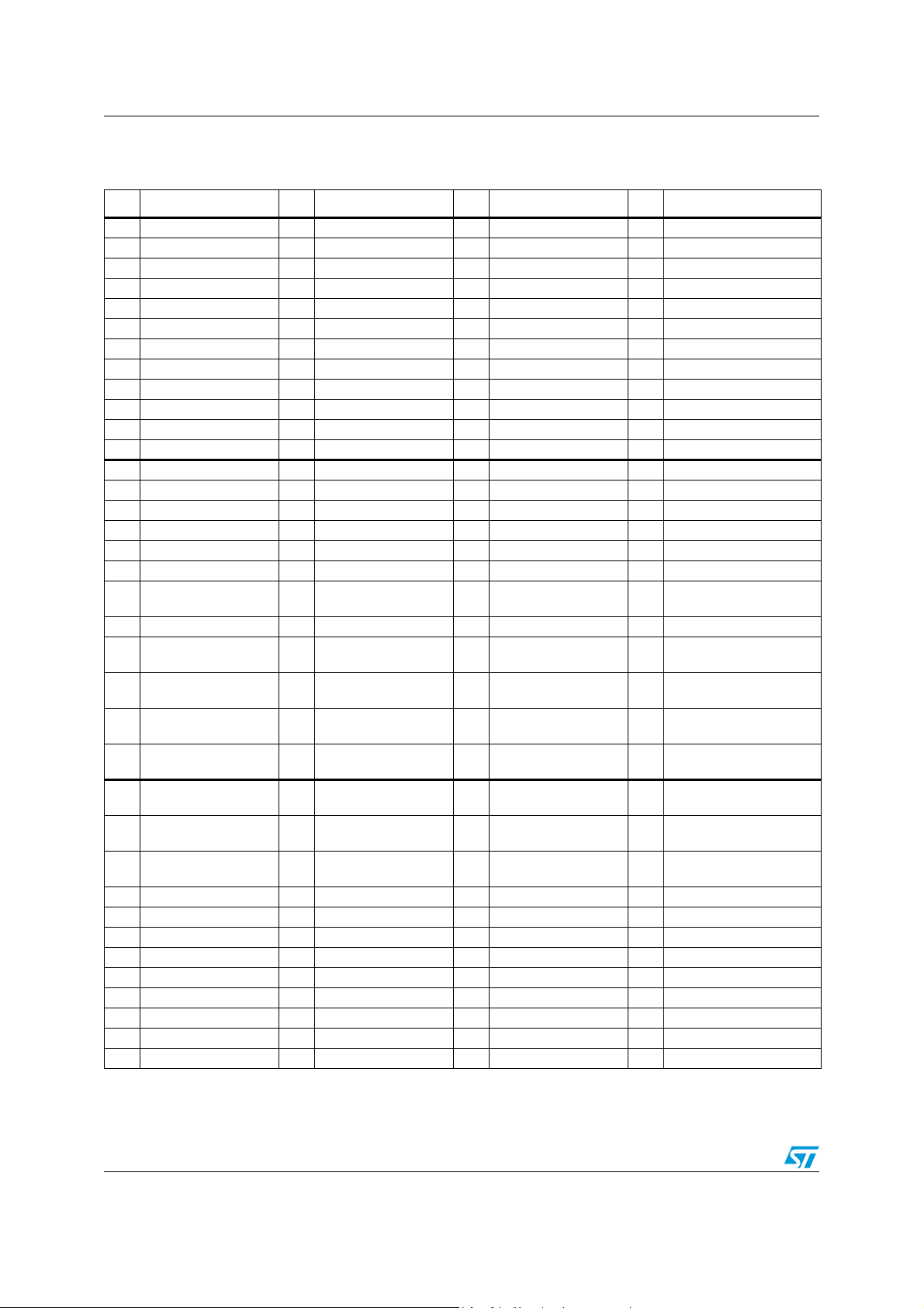
3.2.3 STR731F/STR736F (TQFP100)
Figure 4. STR731F/STR736F pin configuration (top view)
13/52
Page 14
Block diagram STR73xFxx
Legend / Abbreviations for Tab le 4 :
Type: I = input, O = output, S = supply, HiZ= high impedance,
In/Output level: T
= TTL 0.8 V / 2 V with input trigger
T
C
= CMOS 0.3VDD/0.7VDD with input trigger
T
Port and control configuration:
Input: pu/pd = with internal 100 kΩ weak pull-up or pull down
Output: OD = open drain
PP = push-pull
Interrupts:
INTx = external interrupt line
WUPx = wake-up interrupt line
The reset state (during and just after the reset) of the I/O ports is input floating (Input tristate
TTL mode). To avoid excess power consumption, unused I/O ports must be tied to ground.
LFBGA144
Pin name
TQFP100
SS
DD
P0.11/OCMPB
7
Type
T
T
T
T
S Ground
S Supply voltage (5 V)
T
T
T
T
T
T
T
I/O T
T
Table 4. STR73xF pin description
Pin n°
TQFP144
1 A1 1 P0.0/OCMPB2 I/O T
2B22P0.1/OCMPA2I/OT
3C23P0.2/ICAPA2 I/OT
4 C3 4 P0.3/ICAPB2 I/O T
5D1 V
6D2 V
7B15P0.4/OCMPA5I/OT
8 C1 6 P0.5/OCMPB5 I/O T
9D37P0.6/ICAPA5 I/OT
10 D4 P0.7/ICAPB5 I/O T
11 E1 P0.8/OCMPA6 I/O T
12 E2 P0.9/OCMPB6 I/O T
13 E3 P0.10/OCMPA7 I/O T
14 E4
(logic level)
Input Output
pu/pd
Input Level
interrupt
2mA X X Port 0.0 TIM2: output compare B output
2mA X X Port 0.1 TIM2: output compare A output
2mA X X Port 0.2 TIM2: input capture A input
2mA X X Port 0.3 TIM2: input capture B input
2mA X X Port 0.4 TIM5: output compare A output
2mA X X Port 0.5 TIM5: output compare B output
2mA X X Port 0.6 TIM5: input capture A input
2mA X X Port 0.7 TIM5: input capture B input
2mA X X Port 0.8 TIM6: output compare A output
2mA X X Port 0.9 TIM6: output compare B output
2mA X X Port 0.10 TIM7: output compare A output
2mA X X Port 0.11 TIM7: output compare B output
Main
OD
function
(after
PP
reset)
Alternate function
Capability
15 F1 8 V
16 G1 9 V
DD
SS
17 E5 10 P0.12/ICAPA3 I/O T
18 F2 11 P0.13/ICAPB3 I/O T
S Supply voltage (5 V)
S Ground
T
T
14/52
2mA X X Port 0.12 TIM3: input capture A input
2mA X X Port 0.13 TIM3: input capture B input
Page 15
STR73xFxx Block diagram
Table 4. STR73xF pin description
Pin n°
TQFP144
LFBGA144
19 F3 12
Pin name
TQFP100
P0.14/OCMPB
3
Typ e
I/O T
20 F4 13 P0.15/OCMPA3 I/O T
21 F5 14 P1.0/OCMPA4 I/O T
22 F6 15 P1.1/OCMPB4 I/O T
23 G2 16 P1.2/ICAPB4 I/O T
24 G3 17 P1.3/ICAPA4 I/O T
25 G4 V
26 H1 V
SS
DD
S Ground
S Supply voltage (5 V)
27 J1 P1.4 I/O T
28 G5 P1.5 I/O T
29 K1 18 P1.6/OCMPB1 I/O T
30 L1 19 P1.7/OCMPA1 I/O T
31 H2 20 P1.8/OCMPA0 I/O T
32 H3 21 P1.9/OCMPB0 I/O T
33 H4 22 P1.10/ICAPB0 I/O T
34 J2 23 P1.11/ICAPA0 I/O T
35 J3 24 P1.12/ICAPA1 I/O T
36 K2 25 P1.13/ICAPB1 I/O T
37 M1 26 P1.14/CAN0RX I/O T
38 L2 27 P1.15/CAN0TX I/O T
39 L3 28 P2.0/PWM0 I/O T
40 K3 29 P2.1/CAN1RX I/O T
41 M4 30 P2.2/CAN1TX I/O T
42 L4 31 P2.3/PWM1 I/O T
43 M2 32 P2.4/PWM2 I/O T
44 M3 P2.5/PWM3 I/O T
45 K4 P2.6/PWM4 I/O T
46 J4 P2.7/PWM5 I/O T
47 M5 33 M0 I T
48 L5 34 RSTIN I C
49 K5 35 M1 I T
Input Output
Main
function
(after
PP
OD
pu/pd
Input Level
T
T
T
T
T
T
T
T
T
T
T
T
T
T
T
T
T
T
T
T
T
T
T
T
T
T
pd BOOT: mode selection 0 input
T
pu Reset input
T
pd BOOT: mode selection 1 input
T
interrupt
INT0 2mA X X Port 1.8 TIM0: output compare A output
INT1 2mA X X Port 1.9 TIM0: output compare B output
WUP28 2mA X X Port 1.10 TIM0: input capture B input
WUP29 2mA X X Port 1.11 TIM0: input capture A input
WUP30 2mA X X Port 1.12 TIM1: input capture A input
WUP31 2mA X X Port 1.13 TIM1: input capture B input
WUP12 2mA X X Port 1.14 CAN0: receive data input
WUP13 2mA X X Port 2.1 CAN1: receive data input
Capability
2mA X X Port 0.14 TIM3: output compare B output
2mA X X Port 0.15 TIM3: output compare A output
2mA X X Port 1.0 TIM4: output compare A output
2mA X X Port 1.1 TIM4: output compare B output
2mA X X Port 1.2 TIM4: input capture B input
2mA X X Port 1.3 TIM4: input capture A input
2mA X X Port 1.4
2mA X X Port 1.5
2mA X X Port 1.6 TIM1: output compare B output
2mA X X Port 1.7 TIM1: output compare A output
2mA X X Port 1.15 CAN0: transmit data output
2mA X X Port 2.0 PWM0: PWM output
2mA X X Port 2.2 CAN1: transmit data output
2mA X X Port 2.3 PWM1: PWM output
2mA X X Port 2.4 PWM2: PWM output
2mA X X Port 2.5 PWM3: PWM output
2mA X X Port 2.6 PWM4: PWM output
2mA X X Port 2.7 PWM5: PWM output
reset)
Alternate function
15/52
Page 16
Block diagram STR73xFxx
Table 4. STR73xF pin description
Pin n°
Input Output
Main
OD
function
(after
PP
reset)
Alternate function
Oscillator amplifier circuit input and
internal clock generator input.
Pin name
TQFP144
50 J5 36 V
51 M6 37 V
LFBGA144
TQFP100
DD
SS
52 M7 38 XTAL1 I
Typ e
pu/pd
Input Level
interrupt
Capability
S Supply voltage (5 V)
S Ground
53 H5 39 XTAL2 O Oscillator amplifier circuit output.
54 L6 40 V
55 K6 41
SS
P2.8/TDO1/CA
N2RX
S Ground
I/O T
T
2mA X X Port 2.8
UART1:
transmit data
output
CAN2: receive
data input
(TQFP100
only)
CAN2:
56 J6 42
P2.9/RDI1/CAN
2TX
I/O T
UART1:
T
WUP14 2mA X X Port 2.9
receive data
input
transmit data
output
(TQFP100
only)
57 H6 P2.10 I/O T
58 G6 P2.11 I/O T
59 L7 P2.12 I/O T
60 K7 P2.13 I/O T
61 J7 43 P2.14/SCL0 I/O T
62 H7 44 P2.15/SDA0 I/O T
T
T
T
T
T
T
WUP16 2mA X X Port 2.10
WUP17 2mA X X Port 2.11
INT14 2mA X X Port 2.12
INT15 2mA X X Port 2.13
WUP15 2mA X X Port 2.14 I2C0: serial clock
2mA X X Port 2.15 I2C0: serial data
63 M8 45 Test I pd Reserved pin. Must be tied to ground
64 L8 46 V
65 M10 47 V
66 M11 48 V
BIAS
SS
DD
67 K8 P3.0/AIN0 I/O T
68 J8 P3.1/AIN1 I/O T
69 M9 P3.2/AIN2 I/O T
70 L9 P3.3/AIN3 I/O T
71 K9 49 P3.4/AIN4 I/O T
72 L10 50 P3.5/AIN5 I/O T
S
S Ground
S Supply voltage (5 V)
T
T
T
T
T
T
16/52
Internal RC oscillator bias. A 1.3 MΩ
external resistor has to be connected to
this pin when a 32 kHZ RC oscillator
frequency is used.
2mA X X Port 3.0 ADC: analog input 0
2mA X X Port 3.1 ADC: analog input 1
2mA X X Port 3.2 ADC: analog input 2
2mA X X Port 3.3 ADC: analog input 3
2mA X X Port 3.4
2mA X X Port 3.5
ADC: analog input 4
(AIN0 in TQFP100)
ADC: Analog input 5
(AIN1 in TQFP100)
Page 17

STR73xFxx Block diagram
Table 4. STR73xF pin description
Pin n°
Pin name
TQFP144
LFBGA144
TQFP100
Typ e
73 M12 51 P3.6/AIN6 I/O T
74 L11 52 P3.7/AIN7 I/O T
75 K11 53 V
76 K10 54 V
SSA
DDA
S Reference ground for A/D converter
S Reference voltage for A/D converter
77 J12 55 P3.8/AIN8 I/O T
78 J11 56 P3.9/AIN9 I/O T
79 L12 57 P3.10/AIN10 I/O T
80 K12 58 P3.11/AIN11 I/O T
81 J10 59 P3.12/AIN12 I/O T
82 J9 60 P3.13/AIN13 I/O T
83 H12 61 P3.14/AIN14 I/O T
Input Output
pu/pd
Input Level
T
T
T
T
T
T
T
T
T
interrupt
INT2 2mA X X Port 3.12
INT3 2mA X X Port 3.13
INT4 2mA X X Port 3.14
Main
function
(after
PP
OD
reset)
Capability
2mA X X Port 3.6
2mA X X Port 3.7
2mA X X Port 3.8
2mA X X Port 3.9
2mA X X Port 3.10
2mA X X Port 3.11
Alternate function
ADC: analog input 6
(AIN2 in TQFP100)
ADC: analog input 7
(AIN3 in TQFP100)
ADC: analog input 8
(AIN4 in TQFP100)
ADC: analog input 9
(AIN5 in TQFP100)
ADC: analog input 10
(AIN6 in TQFP100)
ADC: analog input 11
(AIN7 in TQFP100)
ADC: analog input 12
(AIN8 in TQFP100)
ADC: analog input 13
(AIN9 in TQFP100)
ADC: analog input 14
(AIN10 in TQFP100)
84 H11 62 P3.15/AIN15 I/O T
85 H10 63 V
86 H9 64 V
DD
SS
S Supply voltage (5 V)
S Ground
87 G12 65 JTRST I T
88 F12 66 JTDI I T
89 H8 67 JTMS I T
90 G11 68 JTCK I T
T
T
T
T
T
INT5 2mA X X Port 3.15
pu JTAG reset Input
pu JTAG data input
pu JTAG mode selection Input
pd JTAG clock Input
91 G10 69 JTDO O 4mA
92 G9 70 V
93 G8 71 V
SS
DD
94 G7 P4.0/ICAPA7 I/O T
95 F11 P4.1/ICAPB7 I/O T
96 F10 P4.2/ICAPA8 I/O T
S Ground
S Supply voltage (5 V)
T
T
T
WUP24 2mA X X Port 4.0 TIM7: input capture A input
WUP25 2mA X X Port 4.1 TIM7: input capture B input
WUP26 2mA X X Port 4.2 TIM8: input capture A input
17/52
ADC: analog input 15
(AIN11 in TQFP100)
JTAG data output.
Note: Reset state = HiZ
Page 18

Block diagram STR73xFxx
Table 4. STR73xF pin description
Pin n°
Pin name
TQFP144
LFBGA144
TQFP100
Typ e
97 F9 P4.3/ICAPB8 I/O T
98 F8 P4.4/CAN2TX I/O T
99 E12 P4.5/CAN2RX I/O T
100 E11 72 P4.6/SCL1 I/O T
101 C12 73 P4.7/SDA1 I/O T
102 B12 P4.8/OCMPA8 I/O T
103 E10 P4.9/ICAPB6 I/O T
104 E9 74
105 D12
P4.10/ICAPA6/I
CAPB5
P4.11/OCMPB
8
I/O T
I/O T
106 D11 P4.12/ICAPA9 I/O T
107 D10 P4.13/ICAPB9 I/O T
108 C11 75 P4.14/SS
1I/OT
109 B11 76 P4.15/SCK1 I/O T
110 B10 77 P5.0/MOSI1 I/O T
Input Output
pu/pd
Input Level
T
T
T
T
T
T
T
T
T
T
T
T
T
T
interrupt
WUP27 2mA X X Port 4.3 TIM8: input capture B input
WUP18 2mA X X Port 4.5 CAN2: receive data input
WUP19 2mA X X Port 4.6 I2C1: serial clock
WUP20 2mA X X Port 4.10
WUP21 2mA X X Port 4.12 TIM9: input capture A input
WUP22 2mA X X Port 4.15 BSPI1: serial clock
Main
OD
function
(after
PP
reset)
Alternate function
Capability
2mA X X Port 4.4 CAN2: transmit data output
2mA X X Port 4.7 I2C1: serial data
2mA X X Port 4.8 TIM8: output compare A output
2mA X X Port 4.9 TIM6: input capture B input
TIM6: input
capture A input
(144-pin pkg
only)
TIM5: input
capture B
input
(TQFP100
only)
2mA X X Port 4.11 TIM8: output compare B output
2mA X X Port 4.13 TIM9: input capture B input
2mA X X Port 4.14 BSPI1: slave select
2mA X X Port 5.0
BSPI1: master output/slave
input
111 C10 78 P5.1/MISO1 I/O T
112 A9 P5.2/OCMPA9 I/O T
113 B9 P5.3/OCMPB9 I/O T
114 C9 79
P5.4/SS
3
2/PWM
115 D9 80 P5.5/SCK2 I/O T
116 A11 81 P5.6/MOSI2 I/O T
117 A10 82 P5.7/MISO2 I/O T
118 A8 83 P5.8/PWM4 I/O T
I/O T
T
T
T
T
T
T
T
T
WUP23 2mA X X Port 5.5 BSPI2: serial clock
INT6 2mA X X Port 5.8
18/52
2mA X X Port 5.1
BSPI1: master input/Slave
output
2mA X X Port 5.2 TIM9: output compare A output
2mA X X Port 5.3 TIM9: output compare B output
PWM3: PWM
2mA X X Port 5.4
BSPI2: slave
select
output
(TQFP100
only)
2mA X X Port 5.6
2mA X X Port 5.7
BSPI2: master output/slave
input
BSPI2: master input/slave
output
PWM4: PWM output (TQFP100
only)
Page 19

STR73xFxx Block diagram
Table 4. STR73xF pin description
Pin n°
Pin name
TQFP144
LFBGA144
TQFP100
Typ e
119 B8 84 P5.9/PWM5 I/O T
120 C8 85 P5.10/RDI2 I/O T
121 A12 86 P5.11/TDO2 I/O T
122 D8 87 P5.12 I/O T
123 E8 P5.13 I/O T
124 B7 P5.14 I/O T
125 A7 P5.15 I/O T
126 A6 88 V
127 C7 89 V
128 D7 90 V
18
SS
DD
S
S Ground
S Supply voltage (5 V)
129 E7 91 P6.0 I/O T
130 F7 P6.1 I/O T
131 B6 92 P6.2/RDI3 I/O T
132 C6 P6.3 I/O T
133 D6 93 P6.4/TDO3 I/O T
134 E6 P6.5 I/O T
135 A5 94 P6.6 I/O T
136 B5 P6.7 I/O T
137 C5 95 P6.8/RDI0 I/O T
138 A3 96 P6.9/TDO0 I/O T
139 A2 P6.10 I/O T
140 D5 97 P6.11/MISO0 I/O T
141 A4 98 P6.12/MOSI0 I/O T
142 B4 99 P6.13/SCK0 I/O T
143 C4 100 P6.14/SS
0I/OT
144 B3 P6.15 I/O T
Input Output
pu/pd
Input Level
T
T
T
T
T
T
T
T
T
T
T
T
T
T
T
T
T
T
T
T
T
T
T
interrupt
INT7 2mA X X Port 5.9
INT8 2mA X X Port 5.10 UART2: receive data input
INT9 2mA X X Port 5.11 UART2: transmit data output
INT10 2mA X X Port 5.12
INT11 2mA X X Port 5.13
INT12 2mA X X Port 5.14
INT13 2mA X X Port 5.15
WUP0 8mA X X Port 6.0
WUP1 2mA X X Port 6.1
WUP2 2mA X X Port 6.2 UART3: receive data input
WUP3 2mA X X Port 6.3
WUP4 2mA X X Port 6.4 UART3: transmit data output
WUP5 2mA X X Port 6.5
WUP6 2mA X X Port 6.6
WUP7 2mA X X Port 6.7
WUP10 2mA X X Port 6.8 UART0: receive data input
WUP8 2mA X X Port 6.10
WUP11 2mA X X Port 6.13 BSPI0: serial clock
WUP9 2mA X X Port 6.15
Main
OD
function
(after
PP
reset)
Alternate function
Capability
PWM5: PWM output (TQFP100
only)
1.8 V decoupling pin: a
decoupling capacitor
(recommended value: 100 nF)
must be connected between this
pin and nearest V
SS pin.
2mA X X Port 6.9 UART0: transmit data output
2mA X X Port 6.11
2mA X X Port 6.12
BSPI0: master input/slave
output
BSPI0: master output/slave
input
2mA X X Port 6.14 BSPI0: slave select
19/52
Page 20

Block diagram STR73xFxx
Flash memory space
64K/128/256 Kbytes
APB BRIDGE 1 REGS
Addressable memory space
0
1
2
3
4
1K
5
6
7
0x1FFF FFFF
0x2000 0000
0x3FFF FFFF
0x4000 0000
0x5FFF FFFF
0x6000 0000
0x7FFF FFFF
0x8000 0000
0x9FFF FFFF
0xA000 0000
0xBFFF FFFF
0xC000 0000
0xDFFF FFFF
0xE000 0000
0xFFFF FFFF
0xFFFF 8000
0xFFFF 83FF
0xFFFF 8400
0xFFFF 87FF
0xFFFF 8800
0xFFFF 8BFF
0xFFFF 8C00
0xFFFF 8FFF
0xFFFF 9000
0xFFFF 93FF
0xFFFF 9400
0xFFFF 97FF
0xFFFF 9800
0xFFFF 9BFF
0xFFFF 9C00
0xFFFF 9FFF
0xFFFF A000
0xFFFF A3FF
0xFFFF A800
0xFFFF ABFF
0xFFFF AC00
0xFFFF AFFF
0xFFFF B000
0xFFFF C3FF
0xFFFF C400
0xFFFF C7FF
0xFFFF C800
0xFFFF CBFF
0xFFFF CC00
0xFFFF D000
0xFFFF FFFF
1K
1K
1K
1K
1K
1K
1K
1K
1K
1K
1K
1K
0x0010 0017
0x6000 03FF
0x0000 0000
APB memory space
4 Gbytes
32 Kbytes
Flash
(1)
64K/128K/256K
PRCCU
1K
APB TO ARM7
BRIDGE
0xFFFF 8000
32K
EIC
0xFFFF FC00
1K
APB BRIDGE 0 REGS
0xFFFF FBFF
0xFFFF CFFF
CONFIG. REGS
64B
Drawing not to scale
0x4000 003F
Flash
0x8010 0017
64K/128K/256K
0xFFFF C000
0xFFFF D400
0xFFFF D3FF
0xFFFF D800
0xFFFF D7FF
0xFFFF DC00
0xFFFF DBFF
0xFFFF E000
0xFFFF DFFF
0xFFFF E400
0xFFFF E3FF
0xFFFF E800
0xFFFF E7FF
0xFFFF EC00
0xFFFF EBFF
1K
1K
1K
1K
1K
1K
1K
1K
1K
1K
1K
1K
I2C 0
reserved
reserved
reserved
TB 0-2
UART 0
UART 1
TIM 0
TIM 1
CAN 0
(4)
CAN 1
(4)
CAN 2
(4)
PWM 0-5
GP I/O 0-6
BSPI 0
BSPI 1
BSPI 2
DMA 0-3
RTC
ADC
0xFFFF F800
0xFFFF F7FF
0xFFFF F400
0xFFFF F3FF
0xFFFF F000
0xFFFF EFFF
0xFFFF B3FF
0xFFFF B400
0xFFFF B7FF
0xFFFF B800
RAM
16K
1K
0xFFFF BBFF
TIM 2
TIM 3
TIM 4
TIM 5-9
reserved
WAKEUP
reserved
1K
0xFFFF BFFF
0xFFFF BC00
I2C 1
access to gray shaded area will return an ABORT
B0F5
(3)
0x8000 1FFF
0x8000 0000
0x8000 2000
0x8000 3FFF
0x8000 4000
0x8000 5FFF
0x8000 6000
0x8000 7FFF
0x8000 8000
0x8000 FFFF
0x8001 0000
0x8001 FFFF
0x8010 0000
0x8010 0017
0x8010 C000
0x8010 DFFF
8K
8K
8K
8K
32K
8K
20B
64K
B0F4
Flash registers
NATIVE ARBITER
16B
B0F6
(2)
0x8002 0000
0x8002 FFFF
64K
B0F7
(2)
0x8003 0000
0x8003 FFFF
64K
UART 2
UART 3
0xFFFF 9E00
0xFFFF A200
CMU
0xFFFF F600
0x2000 000F
System Memory
B0F3
B0F2
B0F1
B0TF
1K
1K
1K
(1) Flash aliased at 0x0000 0000h by system decoder for boot ing with valid instruction upon RESET from Block B0 (8 Kbytes)
0xFFFF A400
0xFFFF A7FF
1K
WDG
WAKEUPTIM
0xFFFF A600
0xA000 3FFF
(2) Only available in STR73xZ2/V2
(3) Only available in STR73xZ2/V2 and STR73xZ1/V1
(4) Only available in STR730/STR731
3.3 Memory mapping
Figure 5 shows the various memory configurations of the STR73xF system. The system
memory map (from 0x0000_0000 to 0xFFFF_FFFF) is shown on the left part of the figure,
the right part shows maps of the Flash and APB areas. For flexibility the Flash or RAM
addresses can be aliased to Block 0 addresses using the remapping feature
Most reserved memory spaces (gray shaded areas in Figure 5) are protected from access
by the user code. When an access this memory space is attempted, an ABORT signal is
generated. Depending on the type of access, the ARM processor will enter “prefetch abort”
state (Exception vector 0x0000_000C) or “data abort” state (Exception vector
0x0000_0010). It is up to the application software to manage these abort exceptions.
Figure 5. Memory map
20/52
Page 21

STR73xFxx Electrical parameters
=50pF
STR7 PIN
V
IN
STR7 PIN
4 Electrical parameters
4.1 Parameter conditions
Unless otherwise specified, all voltages are referred to VSS.
4.1.1 Minimum and maximum values
Unless otherwise specified the minimum and maximum values are guaranteed in the worst
conditions of ambient temperature, supply voltage and frequencies by tests in production on
100% of the devices with an ambient temperature at T
selected temperature range).
Data based on characterization results, design simulation and/or technology characteristics
are indicated in the table footnotes and are not tested in production. Based on
characterization, the minimum and maximum values refer to sample tests and represent the
mean value plus or minus three times the standard deviation (mean±3Σ).
4.1.2 Typical values
Unless otherwise specified, typical data are based on TA=25° C and VDD=5 V. They are
given only as design guidelines and are not tested.
=25° C and TA=T
A
(given by the
Amax
Typical ADC accuracy values are determined by characterization of a batch of samples from
a standard diffusion lot over the full temperature range, where 95% of the devices have an
error less than or equal to the value indicated
4.1.3 Typical curves
Unless otherwise specified, all typical curves are given only as design guidelines and are
not tested.
4.1.4 Loading capacitor
The loading conditions used for pin parameter measurement are shown in Figure 6.
4.1.5 Pin input voltage
The input voltage measurement on a pin of the device is described in Figure 7.
Figure 6. Pin loading conditions Figure 7. Pin input voltage
(mean±2Σ).
21/52
Page 22

Electrical parameters STR73xFxx
4.2 Absolute maximum ratings
Stresses above those listed as “absolute maximum ratings” may cause permanent damage
to the device. This is a stress rating only and functional operation of the device under these
conditions is not implied. Exposure to maximum rating conditions for extended periods may
affect device reliability.
Table 5. Voltage characteristics
Symbol Ratings Min Max Unit
V
|V
V
DD
DDA
|ΔV
SSX
V
V
- V
SSA
- V
IN
DDx
- VSS|
SS
SSA
External 5 V Supply voltage -0.3 6.0
Reference ground for A/D converter V
SS
Reference voltage for A/D converter -0.3
Input voltage on any pin -0.3
Variations between different 5 V
|
power pins
Variations between all the different
ground pins
-0.3
-0.3
V
SS V
+0.3
V
DD
+0.3
V
DD
V
V
mV
V
ESD(HBM)
V
ESD(MM)
Table 6. Current characteristics
Electrostatic discharge voltage
(Human Body Model)
Electrostatic discharge voltage
(Machine Model)
see : Absolute maximum ratings
(electrical sensitivity) on page 36
Symbol Ratings Max. Unit
I
VDD
I
VSS
I
IO
2) & 3)
I
INJ(PIN)
ΣI
INJ(PIN)
1. All 5 V power (VDD, V
supply
2. I
3. Negative injection disturbs the analog performance of the device. See note in Section 4.3.6: 10-bit ADC
4. When several inputs are submitted to a current injection, the maximum
5.) In 144-pin devices, only +10 mA on P0.3, P1.13, P3.6 and P4.13 pins (negative injection not allowed).
must never be exceeded. This is implicitly insured if VIN maximum is respected. If VIN maximum
INJ(PIN)
cannot be respected, the injection current must be limited externally to the I
injection is induced by V
characteristics on page 43.
positive and negative injected currents (instantaneous values). These results are based on
characterization with
Total current into V
power lines (source)
DD
Total current out of VSS ground lines (sink)
Output current sunk by any I/O and control pin 10
Output current source by any I/O and control pin 10
Injected current on any other pin
2)
Total injected current (sum of all I/O and control pins)
) and ground (VSS, V
DDA
while a negative injection is induced by VIN<VSS.
IN>VDD
Σ
I
maximum current injection on four I/O port pins of the device.
INJ(PIN)
4) &5)
) pins must always be connected to the external 5 V
SSA
1)
1)
100
100
±10
Σ
I
INJ(PIN)
4)
INJ(PIN)
is the absolute sum of the
±75
value. A positive
mA
22/52
Page 23

STR73xFxx Electrical parameters
Table 7. Thermal characteristics
Symbol Ratings Value Unit
T
STG
T
J
Storage temperature range -55 to +150 °C
Maximum junction temperature (see Section 5.2: Thermal characteristics on
page 48)
23/52
Page 24

Electrical parameters STR73xFxx
4.3 Operating conditions
Subject to general operating conditions for VDD, and TA.
Table 8. General operating conditions
Symbol Parameter Conditions Min Max Unit
Accessing SRAM or Flash
(zero wait state Flash access
up to 36 MHz)
f
MCLK
V
DD
Internal CPU and system
clock frequency
Standard Operating
Voltage
Operating analog reference
V
DDA
T
A
Table 9. Operating conditions at power-up / power-down
voltage with respect to
ground
Ambient temperature range
6 partnumber suffix
7 partnumber suffix
Symbol Parameter Conditions Min
Subject to general
t
VDD
VDD rise time rate
operating conditions for
.
T
A
036MHz
4.5 5.5 V
4.5 V
-40
-40
Typ
DD
85
105
Max Unit
+0.1 V
°C
-20-ms/V
24/52
Page 25

STR73xFxx Electrical parameters
4.3.1 Supply current characteristics
The current consumption is measured as described in Figure 6 and Figure 7.
Total current consumption
The MCU is placed under the following conditions:
● All I/O pins in input mode with a static value at V
● All peripherals are disabled except if explicitly mentioned.
or VSS (no load)
DD
Subject to general operating conditions for V
DD
Table 10. Total current consumption
Symbol Parameter Conditions
Formula, f
3)
f
RUN mode
WFI mode
= 36 MHz, RAM execution
MCLK
f
= 36 MHz, Flash execution
MCLK
f
= 4 MHz, f
OSC
Main voltage regulator ON,
LP voltage regulator = 2 mA,
RTC and WDG on, other modules off.
f
= high frequency (CMU_RCCTL= 0x8),
RC
= f
f
LPWFI mode
MCLK
LP voltage regulator = 2 mA,
other modules off.
I
DD
= 4 MHz, RC oscillator on
f
OSC
= high frequency (CMU_RCCTL= 0x0)
f
RC
LP voltage regulator = 6 mA,
RTC and WUT ON, other modules off.
Internal wake-up possible.
STOP mode
= high frequency (CMU_RCCTL= 0xF),
f
RC
LP voltage regulator = 2mA.
WUT ON, other modules off.
Internal wake-up possible.
LP voltage regulator = 2 mA, WIU on, Other
modules off, external wake-up.
HALT mode LP voltage regulator = 2 mA. 50 140 µA
in MHz, RAM execution 7 + 1.9 f
MCLK
= f
RC
MCLK
/16,
OSC
, and TA.
/16 = 250 kHz
Typ
1)
MCLK
Max
2)
76 mA
86 mA
6.7 8 mA
220 350 µA
500 700
150 220
50 140
Unit
mA
µA
1. Typical data are based on TA=25° C, VDD=5 V
2. Data based on characterization results, tested in production at V
3. I/O in static configuration (not toggling). RUN mode is almost independent of temperature. On the
contrary RUN mode current is highly dependent on the application. The I
significantly reduced by the application in the following ways: switch-off unused peripherals (default),
reduce peripheral frequency through internal prescaler, fetch the most frequently-used functions from RAM
and use low power mode when possible.
max. and TA = 25° C.
DD
DDRUN
value can be
25/52
Page 26

Electrical parameters STR73xFxx
0
50
100
150
200
250
300
3.5 4 4.5 5 5.5 6 6. 5
Vdd (V)
Idd STOP (µA)
TA=-45°C
TA=25°C
TA=85°C
TA=105°C
0
50
100
150
200
250
300
3.5 4 4.5 5 5.5 6 6.5
Vdd (V)
Idd HALT (µA)
TA=-45°C
TA=25°C
TA=85°C
TA=105°C
5.5
6.0
6.5
7.0
7.5
8.0
3.5 4 4.5 5 5.5 6 6. 5
Vdd (V)
Idd Wfi (mA)
TA= -45 °C
TA= 25° C
TA= 85° C
TA=105°C
0
50
100
150
200
250
300
350
400
450
500
3.5 4 4. 5 5 5.5 6 6.5
Vdd (V)
Idd LPWFI (µA)
TA=-45°C
TA=25°C
TA=85°C
TA=105°C
Figure 8. STOP IDD vs. VDD Figure 9. HALT IDD vs. V
Figure 10. WFI IDD vs. V
DD
Figure 11. LPWFI IDD vs. V
DD
DD
26/52
Page 27

STR73xFxx Electrical parameters
Typical application current consumption
Table 11. Typical consumption in Run mode at 25°C and 85°C
Conditions f
MCLK
(MHz) f
(MHz) Typical I
ADC
10
10
10
VDD= 5.5 V, RC oscillator off,
PLL on, RTC enabled, 1 Timer
(TIM) running, and ADC
running in scan mode.
Code executing in
RAM
Code executing in
Flash
20 29
36 9 42
10
20 32
36 9 48
Table 12. Typical consumption in Run and low power modes at 25°C
Mode Conditions f
RUN All peripherals on, RAM execution
WFI
Main voltage regulator on, Flash on, EIC on, WIU on,
GPIOs on.
PLL off, main voltage regulator on 4 MHz 11 mA
CLOCK2/16, main voltage regulator on 250 kHz 8 mA
SLOW
CLOCK2/16, main voltage regulator off 250 kHz 3 mA
RC oscillator running in low frequency, main crystal
oscillator off, main voltage regulator off
LPWFI
CLOCK2/16, main voltage regulator off, LP voltage
regulator = 2 mA, Flash in power down mode.
Main voltage regulator off, RTC on, RC oscillator off,
LP voltage regulator = 6 mA
MCLK
36 MHz 76 mA
24 MHz 56 mA
36 MHz 33 mA
24 MHz 31 mA
29 kHz 2.5 mA
250 kHz 528 µA
- 378 µA
DD
20
22
Typical I
(mA)
DD
Main voltage regulator off, RTC off, RC oscillator off,
LP voltage regulator = 6 mA
- 83 µA
STOP
Main voltage regulator off, RTC off, RC oscillator off,
LP voltage regulator = 4 mA
Main voltage regulator off, RTC off, RC oscillator off,
LP voltage regulator = 2 mA
- 64 µA
- 44 µA
HALT RTC off, LP voltage regulator = 2 mA - 44 µA
27/52
Page 28

Electrical parameters STR73xFxx
On-chip peripherals
Table 13. Peripheral current consumption at TA= 25°C
Symbol Parameter Conditions Typ Unit
I
DD(RC)
I
DD(TIM)
I
DD(BSPI)
I
DD(UART)
I
DD(I2C)
I
DD(ADC)
I
DD(EIC)
I
DD(CAN)
I
DD(GPIO)
I
DD(TB)
I
DD(PWM)
I
DD(RTC)
I
DD(DMA)
I
DD(ARB)
I
DD(AHB)
I
DD(WUT)
I
DD(WIU)
RC (backup oscillator) supply current
High frequency 120 µA
Low frequency 60 µA
TIM timer supply current
BSPI supply current
UART supply current
I2C supply current
1)
1)
1)
1)
ADC supply current when converting
2)
350 µA
1.1 mA
850 µA
430 µA
5mA
EIC supply current 2.88 mA
CAN supply current
GPIO supply current 150 µA
1)
f
=36 MHz
MCLK
2.95 mA
TB supply current 250 µA
PWM supply current 240 µA
RTC supply current 370 µA
DMA supply current 2.5 mA
Native arbiter supply current 180 µA
AHB arbiter supply current 570 µA
WUT supply current 300 µA
WIU supply current 460 µA
1. Data based on a differential IDD measurement between the on-chip peripheral when kept under reset, not
clocked and the on-chip peripheral when clocked and not kept under reset. This measurement does not
include the pad toggling consumption.
2. Data based on a differential I
conversions.
measurement between reset configuration and continuous A/D
DD
28/52
Page 29

STR73xFxx Electrical parameters
C
L
C
L
Crystal
XTAL1
XTAL2
R
S
Resonator
XTAL1
XTAL2
STR73x
STR73x
STR73x
XTAL1
XTAL2
I
R
F
V
DD
4.3.2 Clock and timing characteristics
Crystal / ceramic resonator oscillator
The STR73xF can operate with a crystal oscillator or resonator clock source. Figure 12 describes a
simple model of the internal oscillator driver as well as example of connection for an oscillator or a
resonator.
Figure 12. Crystal oscillator and resonator
Note: 1 XTAL2 must not be used to directly drive external circuits.
2 For test or boot purpose, XTAL2 can be used as an high impedance input pin to provide an
external clock to the device. XTAL1 should be grounded, and XTAL2 connected to a wave
signal generator providing a 0 to VDD signal. Directly driving XTAL2 may results in
deteriorated jitter and duty cycle.
29/52
Page 30

Electrical parameters STR73xFxx
Main oscillator characteristics
V
= 5 V ± 10%, TA = -40° C to T
DD
Table 14. Main oscillator characteristics
Symbol Parameter Conditions
, unless otherwise specified.
Amax
Val ue
Unit
Min Typ Max
f
OSC
g
V
OSC
V
t
STUP
Oscillator frequency 4 8 MHz
Oscillator
m
transconductance
1)
Oscillation amplitude
Oscillator operating
1)
AV
point
1)
Oscillator start-up time
f
= 4 MHz, TA= 25o C-2.4-
OSC
= 8 MHz, TA= 25o C1.-
f
OSC
Sine wave middle, T
External crystal, V
f
= 4 MHz, TA=-40o C
OSC
External crystal, V
f
= 4 MHz, TA=25o C
OSC
External crystal, V
= 6 MHz, TA=-40o C
f
OSC
External crystal, V
f
= 6 MHz, TA=25o C
OSC
External crystal, V
f
= 8 MHz, TA=-40o C
OSC
External crystal, V
= 8 MHz, TA= 25o C
f
OSC
= 25o C - 0.77 -
A
= 5.5 V,
DD
= 5.0 V,
DD
= 5.5 V,
DD
= 5.0 V,
DD
= 5.5 V,
DD
= 5.0 V,
DD
1.5 4.2 mA/V
--12ms
-5.5 - ms
--8ms
-3.3 - ms
--7ms
-2.7 - ms
V
V
30/52
Page 31

STR73xFxx Electrical parameters
Table 14. Main oscillator characteristics (continued)
Val ue
Symbol Parameter Conditions
3)
C
= C2 4)= 10 pF 150 555 -
1
= C2 = 20 pF 490 1035 -
= 4 MHz
f
OSC
2)
= 10 pF
Cp
f
= 5 MHz
OSC
Cp = 10 pF
f
= 6 MHz
1)
R
Feedback resistor
F
OSC
Cp = 10 pF
f
= 7 MHz
OSC
Cp = 10 pF
f
= 8 MHz
OSC
Cp = 10 pF
C
1
= C2 = 30 pF 490 1030 -
C
1
= C2 = 40 pF 380 850 -
C
1
= C2 = 10 pF 160 470 -
C
1
= C2 = 20 pF 415 800 -
C
1
= C2 = 30 pF 340 735 -
C
1
C
= C2 = 40 pF 260 580 -
1
= C2 = 10 pF 160 415 -
C
1
C
= C2 = 20 pF 325 640 -
1
= C2 = 30 pF 250 550 -
C
1
= C2 = 40 pF 180 420 -
C
1
= C2 = 10 pF 160 375 -
C
1
= C2 = 20 pF 260 525 -
C
1
= C2 = 30 pF 185 420 -
C
1
C
= C2 = 40 pF 135 315 -
1
= C2 = 10 pF 155 340 -
C
1
= C2 = 20 pF 210 435 -
C
1
C
= C2 = 30 pF 145 335 -
1
= C2 = 40 pF 100 245 -
C
1
Min Typ Max
Unit
Ω
1. Min and max values are guaranteed by characterization, not tested in production.
represents the total capacitance between XTAL1 and XTAL2, including the shunt capacitance of the
2. C
P
external quartz crystal as well as the total board parasitic cross-capacitance between XTAL1 track and
XTAL2 track.
represents the total capacitance between XTAL1 and ground, including the external capacitance tied to
3. C
1
XTAL1 pin (C
application board track capacitance to ground and device pin capacitance).
represents the total capacitance between XTAL2 and ground, including the external capacitance tied to
4. C
2
XTAL1 pin (C
application board track capacitance to ground and device pin capacitance).
) as well as the total parasitic capacitance between XTAL1 track and ground (this includes
L
) as well as the total parasitic capacitance between XTAL2 track and ground (this includes
L
31/52
Page 32

Electrical parameters STR73xFxx
RC/backup oscillator characteristics
VDD = 5V ± 10%, TA = -40°C to T
Table 15. RC oscillator characteristics
, unless otherwise specified.
Amax
Symbol Parameter Conditions
High frequency mode
f
RC
RC frequency
Low frequency mode
CMU_RCCTL = 0x0 3 MHz
f
RCHF
RC high frequency
CMU_RCCTL = 0xF 2.3 MHz
CMU_RCCTL = 0x0 35 kHz
f
RCLF
f
RCHFS
f
RCLFS
t
RCSTUP
1) CMU_RCCTL = 0x8
2) RC frequency shift versus average value (%)
RC low frequency
CMU_RCCTL = 0xF 30 kHz
2)
RC high frequency stability Fixed CMU_RCCTL 10 %
2)
RC low frequency stability Fixed CMU_RCCTL 23 %
RC start-up time
Stable V
= 2.35 MHz, TA = 25oC
f
RC
DD
,
Value
Unit
Min Typ Max
1)
1)
2.35 MHz
29 kHz
2.35
µs
32/52
Page 33

STR73xFxx Electrical parameters
PLL electrical characteristics
VDD = 5 V ± 10%, TA = -40° C to T
Table 16. PLL characteristics
, unless otherwise specified
Amax
Symbol Parameter Conditions
f
PLLIN
(1)
PLL reference clock
FREF_RANGE = ‘0’
FREF_RANGE = ‘1’
MX = ”00”
f
PLLOUT
PLL output clock
MX = ”01”
MX = ”10”
MX = ”11”
f
MCLK
System clock DX = 1..7 f
FREF_RANGE = ‘0’, MX0 = ’1’
f
FREE
PLL free running
(2)
frequency
FREF_RANGE = ‘0’, MX0 = ’0’
FREF_RANGE = ‘1’, MX0 = ’1’
FREF_RANGE = ‘1’, MX0 = ’0’
(3)
t
LOCK
Δt
PKJIT
1. f
PLLIN
2. Typical data are based on T
3. Max value is guaranteed by characterization, not tested in production.
PLL lock time
PLL jitter (pk to pk)
is obtained from f
directly or through an optional divider by 2.
OSC
=25°C, VDD=5V
A
Stable oscillator
(f
= 4 MHz), stable V
PLLIN
= 4 MHz (pulse
f
PLLIN
generator)
Min Typ Max
1.5
3.0
20 x f
12 x f
28 x f
16 x f
PLLOUT
DD
Val ue
Unit
3.0
MHz
5.0
PLLIN
PLLIN
PLLIN
PLLIN
MHz
/DX 36 MHz
120
240
240
kHz
480
100 300 μs
1.5 ns
Table 17. Low-power mode wake-up timing
Symbol Parameter Conditions Typ Unit
t
WUHALT
t
WUSTOP
Wake-up from HALT mode 200 µs
RC high frequency in STOP mode 180 µs
Wake-up from STOP mode
RC low frequency in STOP mode 234 µs
Main voltage regulator on
RC oscillator off
f
OSC
= 4 MHz, f
MCLK
= f
OSC
/16
27 µs
RAM or FLASH execution
t
WULPWFI
1)
Wake-up from LPWFI mode
Main voltage regulator on
RC oscillator = high frequency
46 µs
Flash execution
Main voltage regulator on
RC oscillator = low frequency
3.6 ms
Flash execution
1. Flash memory programmed to enter Power Down mode during LPWFI.
33/52
Page 34

Electrical parameters STR73xFxx
4.3.3 Memory characteristics
Flash memory
Table 18. Flash memory characteristics
Val ue
Symbol Parameter Test Conditions
Min Typ
Max
Unit
1)
t
WP
t
DWP
t
BP64
t
BP128
t
BP256
t
SE8
t
SE32
t
SE64
t
RPD
t
PSL
t
ESL
t
ESR
t
SP
t
FPW
N
END
t
RET
Word program (32-bit) 35 80 μs
Double word program(64-bit) 64 150 μs
Bank program (64 K) Double word program 0.5 1.25 s
Bank program (128 K) Double word program 1 2.5 s
Bank program (256 K) Double word program 2 4.9 s
Sector erase (8 K)
Sector erase (32 K)
Sector erase (64 K)
3)
Recovery from power-down 20 μs
3)
Not preprogrammed
Preprogrammed
2)
Not preprogrammed
Preprogrammed
Not preprogrammed
preprogrammed
2)
2)
0.6
0.5
1.1
0.821.8
1.7
1.3
Program suspend latency 10 μs
3)
Erase suspend latency 30 μs
3)
Erase suspend rate
Min. time from erase
resume to next erase
20 20 ms
suspend
3)
Set protection 40 170 µs
3)
First word program 1 ms
Endurance
Data retention TA = 85° C
10 kcycles
20
0.9
0.8
3.7
3.3
s
s
s
Ye a r s
1. TA = -45° C after 0 cycles, Guaranteed by characterization, not tested in production.
2. All bits programmed to 0.
3. Guaranteed by design, not tested in production.
34/52
Page 35

STR73xFxx Electrical parameters
4.3.4 EMC characteristics
Susceptibility tests are performed on a sample basis during product characterization.
Functional EMS (electromagnetic susceptibility)
Based on a simple running application on the product (toggling 2 LEDs through I/O ports),
the product is stressed by two electromagnetic events until a failure occurs (indicated by the
LEDs).
● ESD: Electrostatic discharge (positive and negative) is applied on all pins of the device
until a functional disturbance occurs. This test conforms with the IEC 1000-4-2
standard.
● FTB: A burst of fast transient voltage (positive and negative) is applied to V
through a 100 pF capacitor, until a functional disturbance occurs. This test conforms
with the IEC 1000-4-4 standard.
A device reset allows normal operations to be resumed. The test results are given in the
table below based on the EMS levels and classes defined in application note AN1709.
Designing hardened software to avoid noise problems
EMC characterization and optimization are performed at component level with a typical
application environment and simplified MCU software. It should be noted that good EMC
performance is highly dependent on the user application and the software in particular.
and VSS
DD
Therefore it is recommended that the user applies EMC software optimization and
prequalification tests in relation with the EMC level requested for his application.
Software recommendations:
The software flowchart must include the management of runaway conditions such as:
● Corrupted program counter
● Unexpected reset
● Critical data corruption (control registers...)
Prequalification trials:
Most of the common failures (unexpected reset and program counter corruption) can be
reproduced by manually forcing a low state on the RESET pin or the oscillator pins for 1
second.
To complete these trials, ESD stress can be applied directly on the device, over the range of
specification values. When unexpected behavior is detected, the software can be hardened
to prevent unrecoverable errors occurring (see application note AN1015).
Table 19. EMS data
Symbol Parameter Conditions
=5 V, TA=+25° C, f
V
V
FESD
EFTB
Voltage limits to be applied on any I/O pin
to induce a functional disturbance
Fast transient voltage burst limits to be
applied through 100 pF on V
pins to induce a functional disturbance
DD
and V
V
DD
conforms to IEC 1000-4-2
=5 V, TA=+25° C, f
V
SS
DD
conforms to IEC 1000-4-4
MCLK
MCLK
=36 MHz
=36 MHz
Level/
Class
4A
4A
35/52
Page 36

Electrical parameters STR73xFxx
Electromagnetic interference (EMI)
Based on a simple application running on the product (toggling 2 LEDs through the I/O
ports), the product is monitored in terms of emission. This emission test is in line with the
norm SAE J 1752/3 which specifies the board and the loading of each pin.
Table 20. EMI data
Symbol Parameter Conditions
Monitored
frequency band
Max vs.
[f
OSC4M/fMCLK
Unit
]
6/36 MHz 8/8 MHz
0.1 MHz to 30 MHz 23 30
V
=5.0V,
S
EMI
Peak level
DD
=+25°C,
T
A
All packages
130 MHz to 1 GHz 20 7
dBµV30 MHz to 130 MHz 37 34
SAE EMI Level 4 3.5 -
Absolute maximum ratings (electrical sensitivity)
Based on three different tests (ESD, LU and DLU) using specific measurement methods, the
product is stressed in order to determine its performance in terms of electrical sensitivity.
For more details, refer to the application note AN1181.
Electrostatic discharge (ESD)
Electrostatic discharges (a positive then a negative pulse separated by 1 second) are
applied to the pins of each sample according to each pin combination. The sample size
depends on the number of supply pins in the device (3 parts*(n+1) supply pin). Two models
can be simulated: human body model and machine model. This test conforms to the
JESD22-A114A/A115A standard.
Table 21. ESD Absolute Maximum ratings
Symbol Ratings Conditions
V
ESD(HBM)
V
ESD(MM)
V
ESD(CDM)
Notes:
1. Data based on characterization results, not tested in production.
Electrostatic discharge voltage
(human body model)
Electrostatic discharge voltage
(machine model)
Electrostatic discharge voltage
(charge device model)
Static and dynamic latch-up
● LU: 3 complementary static tests are required on 10 parts to assess the latch-up
performance. A supply overvoltage (applied to each power supply pin) and a current
injection (applied to each input, output and configurable I/O pin) are performed on each
36/52
=+25° C
T
A
Maximum
1)
value
2000
200
750 on corner
pins, 500 on
others
Unit
V
Page 37

STR73xFxx Electrical parameters
sample. This test conforms to the EIA/JESD 78 IC latch-up standard. For more details,
refer to the application note AN1181.
● DLU: Electrostatic discharges (one positive then one negative test) are applied to each
pin of 3 samples when the micro is running to assess the latch-up performance in
dynamic mode. Power supplies are set to the typical values, the oscillator is connected
as near as possible to the pins of the micro and the component is put in reset mode.
This test conforms to the IEC1000-4-2 and SAEJ1752/3 standards. For more details,
refer to the application note AN1181.
Table 22. Electrical sensitivities
Symbol Parameter Conditions
Class
1)
TA=+25°C
=+85°C
LU Static latch-up class
DLU Dynamic latch-up class
1. Class description: A Class is an STMicroelectronics internal specification. All its limits are higher than the
JEDEC specifications, that means when a device belongs to Class A it exceeds the JEDEC standard. B
Class strictly covers all the JEDEC criteria (international standard).
T
A
=+105°C
T
A
= 5.5 V, f
V
DD
TA = +25° C
OSC4M
= 4 MHz, f
MCLK
= 32 MHz,
A
A
A
A
37/52
Page 38

Electrical parameters STR73xFxx
4.3.5 I/O port pin characteristics
General characteristics
Subject to general operating conditions for VDD and TA unless otherwise specified.
Table 23. I/O static characteristics
Symbol Parameter Conditions Min
Typ
Max Unit
V
V
I
INJ(PIN)
ΣI
INJ(PIN)
I
R
R
C
1. Data based on characterization results, not tested in production.
2. When the current limitation is not possible, the V
refer to I
induced by VIN<VSS. Refer to Section 4.2 on page 22 for more details.
3. Leakage could be higher than max. if negative current is injected on adjacent pins.
4. Configuration not recommended, all unused pins must be kept at a fixed voltage: using the output mode of
the I/O for example or an external pull-up or pull-down resistor. Data based on design simulation and/or
technology characteristics, not tested in production.
6. The R
I
PU
Input low level voltage
IL
Input high level voltage
IH
Injected current on any I/O pin ±10 mA
Total injected current (sum of all
I/O and control pins)
2)
Input leakage current
lkg
I
Static current consumption
S
Weak pull-up equivalent
PU
resistor
5)
Weak pull-down equivalent
PD
IO
INJ(PIN)
pull-up and RPD pull-down equivalent resistor are based on a resistive transistor (corresponding
PU
and IPD current characteristics described in Figure 19).
5)
resistor
I/O pin capacitance 5 pF
specification. A positive injection is induced by VIN>V33 while a negative injection is
1)
1)
TTL ports
2.0
0.8
V
±75 mA
3)
V
Floating input
4)
mode
V
V
SS≤VIN≤VDD
±1 μA
200 µA
IN=VSS
IN=VDD
absolute maximum rating must be respected, otherwise
IN
55 120 220 kΩ
55 120 220 kΩ
38/52
Page 39

STR73xFxx Electrical parameters
4.50
4.60
4.70
4.80
4.90
5.00
5.10
01234
Ioh (mA)
VOH(V ) at V DD= 5 V
Ta -45°C
Ta 25°C
Ta 90°C
Ta 110°C
0.00
0.05
0.10
0.15
0.20
0.25
01234
Iol (mA)
VOL(V) at VDD= 5 V
Ta -45°C
Ta 25°C
Ta 90°C
Ta 110°C
Output driving current
Subject to general operating conditions for V
Table 24. Output driving current
I/O Type Symbol Parameter Conditions Min Max Unit
Output low level voltage for an I/O pin
1)
V
OL
when 8 pins are sunk at same time
Standard
Output high level voltage for an I/O pin
2)
V
OH
Med.
V
Current
(JTDO)
High
V
V
OH
Current
P6.0
1. The IIO current sunk must always respect the absolute maximum rating specified in Table 6 and the sum of
IIO (I/O ports and control pins) must not exceed I
2. The I
sum of IIO (I/O ports and control pins) must not exceed IVDD.
V
OH
current sourced must always respect the absolute maximum rating specified in Table 6 and the
IO
when 4 pins are sourced at same time
1)
Output low level voltage for an I/O pin
OL
2)
Output high level voltage for an I/O pin
1)
Output low level voltage for an I/O pin
OL
2)
Output high level voltage for an I/O pin
Figure 13. VOH standard ports vs IOH @ VDD 5V
T
-45° C
A
and TA unless otherwise specified.
DD
.
VSS
Figure 14. V
=+2 mA
I
IO
0.4
IIO=-2 mA VDD-0.8
=+6 mA
I
IO
=-6 mA VDD-0.8
I
IO
=+8 mA
I
IO
=-8 mA VDD-0.8
I
IO
standard ports vs IOL @ VDD 5 V
OL
0.4
0.4
V
39/52
Page 40

Electrical parameters STR73xFxx
4.50
4.60
4.70
4.80
4.90
5.00
5.10
0123456
Ioh (mA)
VOH(V ) at V DD= 5 V
Ta -45°C
Ta 25°C
Ta 90°C
Ta 110°C
0.00
0.02
0.04
0.06
0.08
0.10
0.12
0.14
0 1.2 2.4 3.6 4.8 6
Iol (mA)
VOL(V) at VDD= 5 V
Ta -45°C
Ta 25°C
Ta 90°C
Ta 110°C
4.50
4.60
4.70
4.80
4.90
5.00
5.10
012345678
Ioh (mA)
VOH(V ) at V DD= 5 V
Ta -45°C
Ta 25°C
Ta 90°C
Ta 110°C
0.00
0.02
0.04
0.06
0.08
0.10
0.12
0.14
0.16
0.18
012345678
Iol (mA)
VOL(V) at VDD= 5 V
Ta -45°C
Ta 25°C
Ta 90°C
Ta 110°C
Figure 15. VOH JTDO pin vs IOL @ VDD 5 V Figure 16. VOL JTDO pin vs IOL @ VDD 5 V
Figure 17. VOH P6.0 pin vs IOL @ VDD 5 V Figure 18. VOL P6.0 pin vs IOL @ VDD 5 V
40/52
Page 41

STR73xFxx Electrical parameters
0.01μF
EXTERNAL
RESET
CIRCUIT
Required
STR7X
Filter
R
PU
V
DD
INTERNAL RESET
NRSTIN pin
The NRSTIN pin input driver is CMOS. A permanent pull-up is present which is the same as
R
(see : General characteristics on page 38)
PU
Subject to general operating conditions for
Table 25. Reset pin characteristics
Symbol Parameter Conditions Min
V
and TA unless otherwise specified.
DD
Typ
1)
Max Unit
V
IL(NRSTIN)
V
IH(NRSTIN)
V
hys(NRSTIN)
V
F(RSTINn)
V
NF(RSTINn)
V
RP(RSTINn)
1. Data based on characterization results, not tested in production.
2. Hysteresis voltage between Schmitt trigger switching levels.
3. Data guaranteed by design, not tested in production.
NRSTIN Input low level voltage
NRSTIN Input high level voltage
NRSTIN Schmitt trigger voltage
hysteresis
2)
NRSTIN Input filtered pulse
NRSTIN Input not filtered pulse
NRSTIN removal after Power-up
1)
1)
3)
3)
3)
Figure 19. Recommended NRSTIN pin protection
0.3 V
DD
0.7 V
DD
V
800 mV
500 ns
2µs
100 µs
1)
1. The R
2. The reset network protects the device against parasitic resets.
3. The user must ensure that the level on the NRSTIN pin can go below the V
Table 25. Otherwise the reset will not be taken into account internally.
pull-up equivalent resistor is based on a resistive transistor.
PU
41/52
IL(NRSTIN)
max. level specified in
Page 42

Electrical parameters STR73xFxx
0
50
100
150
200
250
3 3.5 4 4.5 5 5.5
Vdd (v)
Rpu (kOhm )
25C
-45C
110C
Figure 20. NRSTIN RPU vs. V
DD
42/52
Page 43

STR73xFxx Electrical parameters
4.3.6 10-bit ADC characteristics
Subject to general operating conditions for V
Table 26. ADC characteristics
DDA
, f
, and TA unless otherwise specified.
MCLK
Symbol Parameter Conditions Min Typ
f
V
C
t
CAL
ADC
AIN
I
lkg
ADC
t
S
Conversion voltage range
Negative input leakage current on
analog pins
Internal sample and hold
capacitor
2)
Calibration time
3)
Sampling time
2)
| I
V
IN<VSS,
|< 400
IN
µA on adjacent
analog pin
= 10 MHz
f
ADC
f
= 10 MHz
ADC
0.4 10 MHz
V
SSA
114µs
3µs
t
CONV
Total conversion time (including
sampling time)
f
ADC
= 10 MHz
30 (10 for sampling
+20 for successive
approximation)
I
ADC
Running mode Normal mode 5 mA
Power-down mode 1 μA
1)
Max Unit
V
DDA
56μA
3.5 pF
580.2 µs
5802 1/f
1/f
V
ADC
ADC
1. Unless otherwise specified, typical data are based on TA=25°C and V
as design guidelines and are not tested.
2. Calibration is recommended once after each power-up.
3. During the sample time the input capacitance C
source. The internal resistance of the analog source must allow the capacitance to reach its final voltage
level within t
the conversion result. Values for the sample clock t
After the end of the sample time tS, changes of the analog input voltage have no effect on
S.
(6.8 max) can be charged/discharged by the external
AIN
depend on programming.
S
DDA-VSS
=5.0V. They are given only
43/52
Page 44

Electrical parameters STR73xFxx
E
O
E
G
1LSB
IDEAL
1LSB
IDEAL
V
DDAVSSA
–
1024
-----------------------------------------=
V
(1) Example of an actual transfer curve
(2) The ideal transfer curve
(3) End point correlation line
ET=Total Unadjusted Error: maximum deviation
between the actual and the ideal transfer curves.
EO=Offset Error: deviation between the first actual
transition and the first ideal one.
EG=Gain Error: deviation between the last ideal
transition and the last actual one.
ED=Differential Linearity Error: maximum deviation
between actual steps and the ideal one.
EL=Integral Linearity Error: maximum deviation
between any actual transition and the end point
correlation line.
1023
1022
1021
5
4
3
2
1
0
7
6
1234567
1021 1022 1023 1024
(1)
(2)
E
T
E
D
E
L
(3)
V
DDA
V
SSA
AINx
STR73X
V
DD
I
L
±1μA
V
T
0.6V
V
T
0.6V
C
ADC
3.5pF
V
AIN
R
AIN
10-Bit A/D
conversion
2.3kΩ(max)
C
AIN
Table 27. ADC accuracy with f
V
=5 V. This assumes that the ADC is calibrated
DDA
Symbol Parameter Conditions Typ Max Unit
MCLK
= 20 MHz, f
=10 MHz, R
ADC
< 10 kΩ RAIN,
AIN
2)
1)
1)
1.0 2.0
0.15 1.0
0.97 1.1
1)
0.7 1.0
LSB
0.76 1.5
INJ(PIN)
and ΣI
in Section 4.3.5 does not
INJ(PIN)
|E
|
Total unadjusted error
T
|EO|
|E
|E
|EL|
1. ADC accuracy vs. negative injection current: Injecting negative current on any of the standard (non-robust)
analog input pins should be avoided as this significantly reduces the accuracy of the conversion being
performed on another analog input. It is recommended to add a Schottky diode (pin to ground) to standard
analog pins which may potentially inject negative current. The effect of negative injection current on robust
pins is specified in Section 4.3.5.
Any positive injection current within the limits specified for I
affect the ADC accuracy.
Offset error
|
Gain error
G
|
Differential linearity error
D
Integral linearity error
1)
1)
2. Calibration is needed once after each power-up.
Figure 21. ADC accuracy characteristics
Figure 22. Typical application with ADC
44/52
Page 45

STR73xFxx Electrical parameters
V
SS
V
DD
0.1 μF
5V
STR73x
V
DDA
V
SSA
POWER
SUPPLY
SOURCE
STR7
DIGITAL NOISE
FILTERING
EXTERNAL
NOISE
FILTERING
1 to 10 μF
0.1 μF
Analog power supply and reference pins
The V
DDA
and V
pins are the analog power supply of the A/D converter cell. They act as
SSA
the high and low reference voltages for the conversion.
Separation of the digital and analog power pins allow board designers to improve A/D
performance. Conversion accuracy can be impacted by voltage drops and noise in the event
of heavily loaded or badly decoupled power supply lines (see: General PCB design
guidelines).
General PCB design guidelines
To obtain best results, some general design and layout rules should be followed when
designing the application PCB to shield the noise-sensitive, analog physical interface from
noise-generating CMOS logic signals.
● Use separate digital and analog planes. The analog ground plane should be connected
to the digital ground plane via a single point on the PCB.
● Filter power to the analog power planes. It is recommended to connect capacitors, with
good high frequency characteristics, between the power and ground lines,
0.1 µF and optionally, if needed 10 pF capacitors as close as possible to the STR7
power supply pins and a 1 to 10 µF capacitor close to the power source (see
Figure 23).
● The analog and digital power supplies should be connected in a star network. Do not
use a resistor, as V
used as a reference voltage by the A/D converter and any
DDA is
resistance would cause a voltage drop and a loss of accuracy.
● Properly place components and route the signal traces on the PCB to shield the analog
inputs. Analog signals paths should run over the analog ground plane and be as short
as possible. Isolate analog signals from digital signals that may switch while the analog
inputs are being sampled by the A/D converter. Do not toggle digital outputs near the
A/D input being converted.
placing
Software filtering of spurious conversion results
For EMC performance reasons, it is recommended to filter A/D conversion outliers using
software filtering techniques.
Figure 23. Power supply filtering
45/52
Page 46

Package characteristics STR73xFxx
Dim.
mm inches
(1)
Min Typ Max Min Typ Max
A 1.60 0.0630
A1 0.05 0.15 0.0020 0.0059
A2 1.35 1.40 1.45 0.0531 0.0551 0.0571
b 0.17 0.22 0.27 0.0067 0.0087 0.0106
C 0.09 0.20 0.0035 0.0079
D 16.00 0.6299
D1 14.00 0.5512
E 16.00 0.6299
E1 14.00 0.5512
e 0.50 0.0197
h 0° 3.5° 7° 0° 3.5° 7°
L 0.45 0.60 0.75 0.0177 0.0236 0.0295
L1 1.00 0.0394
Number of Pins
N 100
1. Values in inches are converted from mm and
rounded to 4 decimal digits.
h
c
L
L1
e
b
A
A2
A1
D
D1
E
E1
Dim.
mm inches
(1)
1. Values in inches are converted from mm
and rounded to 4 decimal digits.
Min Typ Max Min Typ Max
A 1.60 0.0630
A1 0.05 0.15 0.0020 0.0059
A2 1.35 1.40 1.45 0.0531 0.0551 0.0571
b 0.17 0.22 0.27 0.0067 0.0087 0.0106
c 0.09 0.20 0.0035 0.0079
D 21.80 22.00 22.20 0.8583 0.8661 0.8740
D1 19 .80 20.00 20.20 0.7795 0.7874 0.7953
D3 17.50 0.6890
E 21.80 22.00 22.20 0.8583 0.8661 0.8740
E1 19.80 20.00 20.20 0.7795 0.7874 0.7953
E3 17.50 0.6890
e 0.50 0.0197
K 0° 3.5° 7° 0° 3.5° 7°
L 0.45 0.60 0.75 0.0177 0.0236 0.0295
L1 1.00 0.0394
Number of Pins
N 144
A
A2
A1
b
c
36
37
72
73108
109
144
E1
E
D1
D
1
h
b
L
L1
Seating Plane
0.10mm
.004 in.
e
E3
D3
5 Package characteristics
5.1 Package mechanical data
Figure 24. 100-pin thin quad flat package
Figure 25. 144-pin thin quad flat package
46/52
Page 47

STR73xFxx Package characteristics
Dim.
mm inches
1)
Min Typ Max Min Typ Max
A 1.21 1.70 0.0476 0.0669
A1 0.21 0.0083
A2 1.085 0.0427
b 0.35 0.40 0.45 0.0138 0.0157 0.0177
D 9.85 10.00 10.15 0.3878 0.3937 0.3996
D1 8.80 0.3465
E 9.85 10.00 10.15 0.3878 0.3937 0.3996
E1 8.80 0.3465
e 0.80 0.0315
F 0.60 0.0236
ddd 0.10 0.0039
eee 0.15 0.0059
fff 0.08 0.0031
Number of Pins
N 144
1
Values in inches are converted from mm and
rounded to 4 decimal digits.
Dpad
Dsm
Dpad 0.37 mm
Dsm
0.52 mm typ. (depends on solder
mask registration tolerance
Solder paste 0.37 mm aperture diameter
– Non solder mask defined pads are recommended
– 4 to 6 mils screen print
Figure 26. 144-ball low profile fine pitch ball grid array package
Figure 27. Recommended PCB design rules (0.80/0.75mm pitch BGA)
47/52
Page 48

Package characteristics STR73xFxx
5.2 Thermal characteristics
The average chip-junction temperature, TJ, in degrees Celsius, may be calculated using the
following equation:
T
= TA + (PD x ΘJA)(1)
J
Where:
–T
– Θ
–P
–P
–P
Most of the time for the applications P
P
may be significant if the device is configured to drive continuously external modules
I/O
and/or memories.
is the ambient temperature in °C,
A
is the package junction-to-ambient thermal resistance, in °C/W,
JA
is the sum of P
D
is the product of I
INT
INT
and P
and VDD, expressed in Watts. This is the chip internal
DD
I/O (PD
= P
INT
+ P
I/O
),
power,
represents the power dissipation on input and output pins; user determined.
I/O
I/O< PINT
and may be neglected. On the other hand,
An approximate relationship between P
P
= K / (TJ + 273°C) (2)
D
and TJ (if P
D
is neglected) is given by:
I/O
Therefore (solving equations 1 and 2):
K = P
x (TA + 273°C) + ΘJA x P
D
2
(3)
D
Where:
– K is a constant for the particular part, which may be determined from equation (3)
by measuring P
of P
and TJ may be obtained by solving equations (1) and (2) iteratively for any
D
value of T
Table 28. Thermal characteristics
Symbol Description Package Value (typical) Unit
Θ
JA
A
Thermal resistance junction-ambient
(at equilibrium) for a known TA. Using this value of K, the values
D
LFBGA144 50
TQFP100 40
°C/WTQFP144 40
48/52
Page 49

STR73xFxx Order codes
6 Order codes
Table 29. Order codes
Partnumber
STR730FZ1T6 128
STR730FZ2T6 256
STR730FZ1H6 128
STR730FZ2H6 256
STR735FZ1T6 128
STR735FZ2T6 256
STR735FZ1H6 128
STR735FZ2H6 256
STR731FV0T6 64
STR731FV1T6 128
STR731FV2T6 256
STR736FV0T6 64
STR736FV2T6 256
Flash
Kbytes
Package
TQFP144
20x20
LFBGA144
10x10
TQFP144
20x20
LFBGA144
10x10
TQFP100
14x14
TQFP100
14x14
RAM
Kbytes
16
TIM
timers
10
6
6x PWM
module
1
CAN
periph
3
0
3
0STR736FV1T6 128
A/D
Wake-up
chan.
16 32 112
12 18 72
lines
I/O
ports
Tem p.
range
-40 to
+85°C
STR730FZ1T7 128
STR730FZ2T7 256
STR730FZ1H7 128
STR730FZ2H7 256
STR735FZ1T7 128
STR735FZ2T7 256
STR735FZ1H7 128
STR735FZ2H7 256
STR731FV0T7 64
STR731FV1T7 128
STR731FV2T7 256
STR736FV0T7 64
STR736FV2T7 256
TQFP144
20x20
LFBGA144
10x10
TQFP144
20x20
LFBGA144
10x10
TQFP100
14x14
TQFP100
14x14
16
10
3
16 32 112
0
1
3
6
0STR736FV1T7 128
12 18 72
-40 to
+105°C
49/52
Page 50

Known limitations STR73xFxx
7 Known limitations
7.1 Low power wait for interrupt mode
When the STR73x device is put in Low Power Wait For Interrupt mode (LPWFI), the Flash
goes into low power mode or power down mode, depending on the setting of the PWD bit in
the Flash Control Register 0 (default is ‘0’, Low Power mode). This default mode can create
excessive voltage conditions on the transistor gates and may affect the long term behavior
of the Low Power mode circuitry.
Workaround
There is no workaround. If Low Power Wait For Interrupt mode is used, it is strongly
suggested to configure the Flash to enter power down mode (bit PWD = ‘1’).
7.2 PLL free running mode at high temperature
When the STR73x device is operated and an ambient temperature (TA) of more than 55° C
and the main system clock (f
may not work properly.
) is sourced by the PLL in free running mode, the device
MCLK
Workaround
At high temperature (more than 55° C), it is recommended to use the internal RC oscillator
as a backup clock source rather than the PLL free running mode.
50/52
Page 51

STR73xFxx Revision history
8 Revision history
Table 30. Document revision history
Date Revision Description of changes
19-Sep-2005 1 First release
02-Nov-2005 2
08-Mar-2006 3
04-Jun-2006 4
19-Jun-2006 5
08-Sep-2006 6
08-Jun-2008 7
Removed Table 8 power consumption in LP modes
Updated PLL frequency in Section 1.1 and Ta bl e 1 2
Section 3.4: Preliminary power consumption data updated
Section 3.5: DC electrical characteristics updated
Section 7: Known limitations added
Section 4: Electrical parameters updated
Section 7: Known limitations updated
Added temperature range -40°C to 85°C in Section 6: Order
codes
Changed Flash data retention to 20 years at 85°C in Table 18 on
page 34.
Changed Table 24: Output driving current on page 39
Added Figure 14: VOL standard ports vs IOL @ VDD 5 V thru
Figure 18: VOL P6.0 pin vs IOL @ VDD 5 V on page 40.
Added Figure 20: NRSTIN RPU vs. VDD
Inch values rounded to 4 decimal digits in Section 5.1: Package
mechanical data
Modified BSPI speed in Section 2.1: On-chip peripherals
51/52
Page 52

STR73xFxx
Please Read Carefully:
Information in this document is provided solely in connection with ST products. STMicroelectronics NV and its subsidiaries (“ST”) reserve the
right to make changes, corrections, modifications or improvements, to this document, and the products and services described herein at any
time, without notice.
All ST products are sold pursuant to ST’s terms and conditions of sale.
Purchasers are solely responsible for the choice, selection and use of the ST products and services described herein, and ST assumes no
liability whatsoever relating to the choice, selection or use of the ST products and services described herein.
No license, express or implied, by estoppel or otherwise, to any intellectual property rights is granted under this document. If any part of this
document refers to any third party products or services it shall not be deemed a license grant by ST for the use of such third party products
or services, or any intellectual property contained therein or considered as a warranty covering the use in any manner whatsoever of such
third party products or services or any intellectual property contained therein.
UNLESS OTHERWISE SET FORTH IN ST’S TERMS AND CONDITIONS OF SALE ST DISCLAIMS ANY EXPRESS OR IMPLIED
WARRANTY WITH RESPECT TO THE USE AND/OR SALE OF ST PRODUCTS INCLUDING WITHOUT LIMITATION IMPLIED
WARRANTIES OF MERCHANTABILITY, FITNESS FOR A PARTICULAR PURPOSE (AND THEIR EQUIVALENTS UNDER THE LAWS
OF ANY JURISDICTION), OR INFRINGEMENT OF ANY PATENT, COPYRIGHT OR OTHER INTELLECTUAL PROPERTY RIGHT.
UNLESS EXPRESSLY APPROVED IN WRITING BY AN AUTHORIZED ST REPRESENTATIVE, ST PRODUCTS ARE NOT
RECOMMENDED, AUTHORIZED OR WARRANTED FOR USE IN MILITARY, AIR CRAFT, SPACE, LIFE SAVING, OR LIFE SUSTAINING
APPLICATIONS, NOR IN PRODUCTS OR SYSTEMS WHERE FAILURE OR MALFUNCTION MAY RESULT IN PERSONAL INJURY,
DEATH, OR SEVERE PROPERTY OR ENVIRONMENTAL DAMAGE. ST PRODUCTS WHICH ARE NOT SPECIFIED AS "AUTOMOTIVE
GRADE" MAY ONLY BE USED IN AUTOMOTIVE APPLICATIONS AT USER’S OWN RISK.
Resale of ST products with provisions different from the statements and/or technical features set forth in this document shall immediately void
any warranty granted by ST for the ST product or service described herein and shall not create or extend in any manner whatsoever, any
liability of ST.
ST and the ST logo are trademarks or registered trademarks of ST in various countries.
Information in this document supersedes and replaces all information previously supplied.
The ST logo is a registered trademark of STMicroelectronics. All other names are the property of their respective owners.
© 2008 STMicroelectronics - All rights reserved
STMicroelectronics group of companies
Australia - Belgium - Brazil - Canada - China - Czech Republic - Finland - France - Germany - Hong Kong - India - Israel - Italy - Japan -
Malaysia - Malta - Morocco - Singapore - Spain - Sweden - Switzerland - United Kingdom - United States of America
www.st.com
52/52
 Loading...