

Page 1
ARM7TDMI™ 32-bit MCU with Flash, USB, CAN
5 timers, ADC, 10 communications interfaces
Features
■ Core
– ARM7TDMI 32-bit RISC CPU
– 59 MIPS @ 66 MHz from SRAM
– 45 MIPS @ 50 MHz from Flash
■ Memories
– Up to 256 Kbytes Flash program memory
(10 kcycles endurance, 20 years retention
@ 85° C)
– 16 Kbytes Flash data memory
(100 kcycles endurance, 20 years
retention@ 85° C)
– Up to 64 Kbytes RAM
– External Memory Interface (EMI) for up to 4
banks of SRAM, Flash, ROM
– Multi-boot capability
■ Clock, reset and supply management
– 3.0 to 3.6V application supply and I/Os
– Internal 1.8V regulator for core supply
– Clock input from 0 to 16.5 MHz
– Embedded RTC osc. running from external
32 kHz crystal
– Embedded PLL for CPU clock
– Realtime Clock for clock-calendar function
– 5 power saving modes: SLOW, WAIT,
LPWAIT, STOP and STANDBY modes
■ Nested interrupt controller
– Fast interrupt handling with multiple vectors
– 32 vectors with 16 IRQ priority levels
– 2 maskable FIQ sources
■ Up to 48 I/O ports
– 30/32/48 multifunctional bidirectional I/Os
Up to 14 ports with interrupt capability
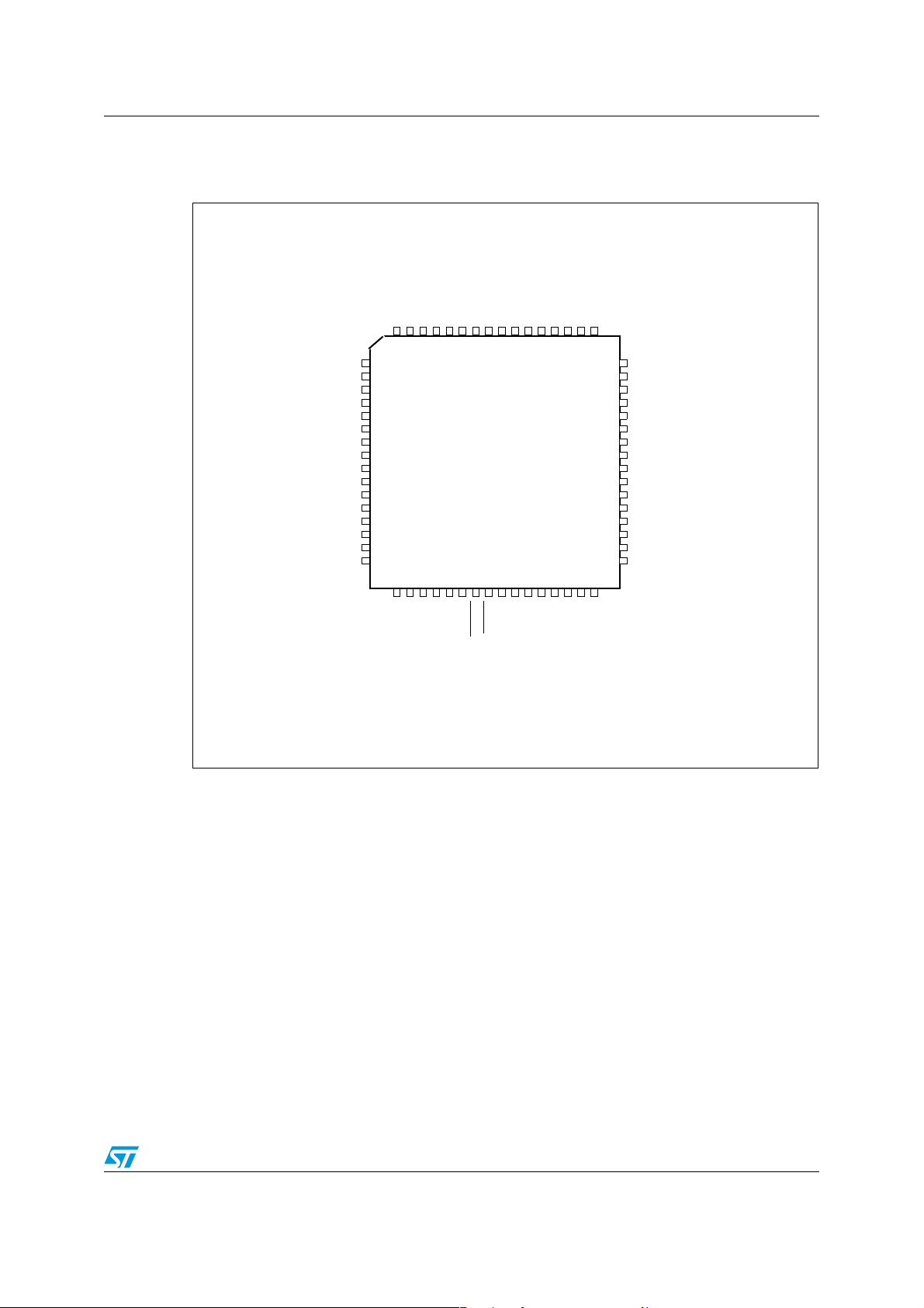
STR71xF
LQFP64
10 x 10
LFBGA64 8 x 8 x 1.7
LFBGA64 8 x 8 x 1.7
■ 5 Timers
– 16-bit watchdog timer
– 3 16-bit timers with 2 input captures, 2
output compares, PWM and pulse counter
– 16-bit timer for timebase functions
■ 10 communications interfaces
2
–2 I
C interfaces (1 multiplexed with SPI)
– 4 UART asynchronous serial interfaces
– Smartcard ISO7816-3 interface on UART1
– 2 BSPI synchronous serial interfaces
– CAN interface (2.0B Active)
– USB Full Speed (12 Mbit/s) Device
Function with Suspend and Resume
– HDLC synchronous communications
■ 4-channel 12-bit A/D converter
– Sampling frequency up to 1 kHz
– Conversion range: 0 to 2.5 V
■ Development tools support
– Atomic bit SET and RES operations
Table 1. Device summary
Reference Root part number
STR710FZ1, STR710FZ2,
STR71xF
STR711FR0, STR711FR1, STR711FR2,
STR712FR0, STR712FR1, STR712FR2,
STR715FR0
LQFP144
20 x 20
LFBGA144 10 x 10 x 1.7
February 2008 Rev 12 1/78
www.st.com
78
Page 2

Contents STR71xF
Contents
1 Introduction . . . . . . . . . . . . . . . . . . . . . . . . . . . . . . . . . . . . . . . . . . . . . . . . 4
2 Description . . . . . . . . . . . . . . . . . . . . . . . . . . . . . . . . . . . . . . . . . . . . . . . . . 5
3 System architecture . . . . . . . . . . . . . . . . . . . . . . . . . . . . . . . . . . . . . . . . . 6
3.1 On-chip peripherals . . . . . . . . . . . . . . . . . . . . . . . . . . . . . . . . . . . . . . . . . . 7
3.2 Related documentation . . . . . . . . . . . . . . . . . . . . . . . . . . . . . . . . . . . . . . 10
3.3 Pin description for 144-pin packages . . . . . . . . . . . . . . . . . . . . . . . . . . . . 11
3.4 Pin description for 64-pin packages . . . . . . . . . . . . . . . . . . . . . . . . . . . . . 21
3.5 External connections . . . . . . . . . . . . . . . . . . . . . . . . . . . . . . . . . . . . . . . . 28
3.6 I/O port configuration . . . . . . . . . . . . . . . . . . . . . . . . . . . . . . . . . . . . . . . . 29
3.7 Memory mapping . . . . . . . . . . . . . . . . . . . . . . . . . . . . . . . . . . . . . . . . . . . 30
4 Electrical parameters . . . . . . . . . . . . . . . . . . . . . . . . . . . . . . . . . . . . . . . 33
4.1 Parameter conditions . . . . . . . . . . . . . . . . . . . . . . . . . . . . . . . . . . . . . . . . 33
4.1.1 Minimum and maximum values . . . . . . . . . . . . . . . . . . . . . . . . . . . . . . . 33
4.1.2 Typical values . . . . . . . . . . . . . . . . . . . . . . . . . . . . . . . . . . . . . . . . . . . . . 33
4.1.3 Typical curves . . . . . . . . . . . . . . . . . . . . . . . . . . . . . . . . . . . . . . . . . . . . 33
4.1.4 Loading capacitor . . . . . . . . . . . . . . . . . . . . . . . . . . . . . . . . . . . . . . . . . 33
4.1.5 Pin input voltage . . . . . . . . . . . . . . . . . . . . . . . . . . . . . . . . . . . . . . . . . . 33
4.2 Absolute maximum ratings . . . . . . . . . . . . . . . . . . . . . . . . . . . . . . . . . . . . 34
4.3 Operating conditions . . . . . . . . . . . . . . . . . . . . . . . . . . . . . . . . . . . . . . . . 36
4.3.1 Supply current characteristics . . . . . . . . . . . . . . . . . . . . . . . . . . . . . . . . 37
4.3.2 Clock and timing characteristics . . . . . . . . . . . . . . . . . . . . . . . . . . . . . . 41
4.3.3 Memory characteristics . . . . . . . . . . . . . . . . . . . . . . . . . . . . . . . . . . . . . 46
4.3.4 EMC characteristics . . . . . . . . . . . . . . . . . . . . . . . . . . . . . . . . . . . . . . . . 47
4.3.5 I/O port pin characteristics . . . . . . . . . . . . . . . . . . . . . . . . . . . . . . . . . . . 50
4.3.6 TIM timer characteristics . . . . . . . . . . . . . . . . . . . . . . . . . . . . . . . . . . . . 56
4.3.7 EMI - external memory interface . . . . . . . . . . . . . . . . . . . . . . . . . . . . . . 56
4.3.8 I2C - inter IC control interface . . . . . . . . . . . . . . . . . . . . . . . . . . . . . . . . 60
4.3.9 BSPI - buffered serial peripheral interface . . . . . . . . . . . . . . . . . . . . . . . 63
4.3.10 USB characteristics . . . . . . . . . . . . . . . . . . . . . . . . . . . . . . . . . . . . . . . . 65
4.3.11 ADC characteristics . . . . . . . . . . . . . . . . . . . . . . . . . . . . . . . . . . . . . . . . 66
2/78
Page 3

STR71xF Contents
5 Package characteristics . . . . . . . . . . . . . . . . . . . . . . . . . . . . . . . . . . . . . 69
5.1 Package mechanical data . . . . . . . . . . . . . . . . . . . . . . . . . . . . . . . . . . . . 69
5.2 Thermal characteristics . . . . . . . . . . . . . . . . . . . . . . . . . . . . . . . . . . . . . . 72
6 Product history . . . . . . . . . . . . . . . . . . . . . . . . . . . . . . . . . . . . . . . . . . . . 73
7 Ordering information . . . . . . . . . . . . . . . . . . . . . . . . . . . . . . . . . . . . . . . 75
8 Revision history . . . . . . . . . . . . . . . . . . . . . . . . . . . . . . . . . . . . . . . . . . . 76
Note: For detailed information on the STR71x Microcontroller memory, registers and peripherals,
please refer to the STR71x Reference Manual.
3/78
Page 4
Introduction STR71xF
1 Introduction
This datasheet provides the STR71x pinout, ordering information, mechanical and electrical
device characteristics.
For complete information on the STR71x microcontroller memory, registers and peripherals.
please refer to the STR71x reference manual.
For information on programming, erasing and protection of the internal Flash memory
please refer to the STR7 Flash programming reference manual.
For information on the ARM7TDMI core please refer to the ARM7TDMI technical reference
manual.
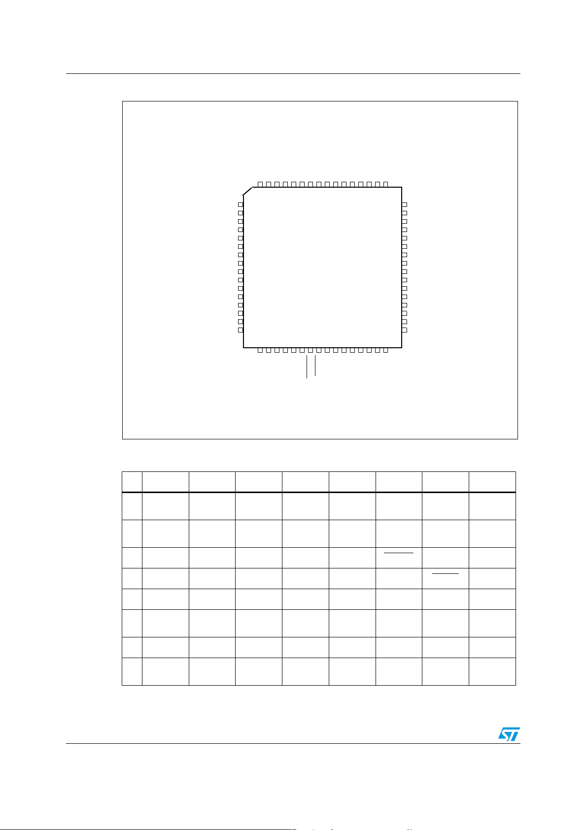
Table 2. Device overview
Features
Flash - Kbytes 128+16 256+16 0 64+16 128+16 256+16 64+16 128+16 256+16 64+16
RAM - Kbytes 32 64 64 16 32 64 16 32 64 16
Peripheral
Functions
Operating
Voltage
Operating
Temperature
Packages
STR710
FZ1
STR710
FZ2
STR710RZSTR711
FR0
STR711
FR1
STR711
FR2
STR712
FR0
STR712
FR1
STR712
FR2
CAN, EMI, USB, 48 I/Os USB, 30 I/Os CAN, 32 I/Os 32 I/Os
3.0 to 3.6 V
-40 to +85°C or 0 to 70° C
T=LQFP144 20 x 20
H=LFBGA144 10 x10
T=LQFP64 10 x10 / H=LFBGA64 8 x 8 x 1.7
STR715
FRx
.
4/78
Page 5

STR71xF Description
2 Description
ARM® core with embedded Flash and RAM
The STR71x series is a family of ARM-powered 32-bit microcontrollers with embedded
Flash and RAM. It combines the high performance ARM7TDMI CPU with an extensive
range of peripheral functions and enhanced I/O capabilities. STR71xF devices have on-chip
high-speed single voltage FLASH memory and high-speed RAM. STR710R devices have
high-speed RAM but no internal Flash. The STR71x family has an embedded ARM core and
is therefore compatible with all ARM tools and software.
Extensive tools support
STMicroelectronics’ 32-bit, ARM core-based microcontrollers are supported by a complete
range of high-end and low-cost development tools to meet the needs of application
developers. This extensive line of hardware/software tools includes starter kits and complete
development packages all tailored for ST’s ARM core-based MCUs. The range of
development packages includes third-party solutions that come complete with a graphical
development environment and an in-circuit emulator/programmer featuring a JTAG
application interface. These support a range of embedded operating systems (OS), while
several royalty-free OSs are also available.
For more information, please refer to ST MCU site http://www.st.com/mcu
5/78
Page 6

System architecture STR71xF
3 System architecture
Package choice: low pin-count 64-pin or feature-rich 144-pin LQFP or BGA
The STR71x family is available in 5 main versions.
The 144-pin versions have the full set of all features including CAN, USB and External
Memory Interface (EMI).
● STR710F: 144-pin BGA or LQFP with CAN, USB and EMI
● STR710R: Flashless 144-pin BGA or LQFP with CAN, USB and EMI (no internal Flash
memory)
The three 64-pin versions (BGA or LQFP) do not include External Memory Interface.
● STR715F: 64-pin BGA or LQFP without CAN or USB
● STR711F: 64-pin BGA or LQFP with USB
● STR712F: 64-pin BGA or LQFP with CAN
High speed Flash memory (STR71xF)
The Flash program memory is organized in two banks of 32-bit wide Burst Flash memories
enabling true read-while-write (RWW) operation. Device Bank 0 is up to 256 Kbytes in size,
typically for the application program code. Bank 1 is 16 Kbytes, typically used for storing
data constants. Both banks are accessed by the CPU with zero wait states @ 33 MHz
Bank 0 memory endurance is 10K write/erase cycles and Bank 1 endurance is 100K
write/erase cycles. Data retention is 20 years at 85°C on both banks. The two banks can be
accessed independently in read or write. Flash memory can be accessed in two modes:
● Burst mode: 64-bit wide memory access at up to 50 MHz.
● Direct 32-bit wide memory access for deterministic operation at up to 33 MHz.
The STR7 embedded Flash memory can be programmed using In-Circuit Programming or
In-Application programming.
IAP (in-application programming): The IAP is the ability to re-program the Flash memory
of a microcontroller while the user program is running.
ICP (in-circuit programming): The ICP is the ability to program the Flash memory of a
microcontroller using JTAG protocol while the device is mounted on the user application
board.
The Flash memory can be protected against different types of unwanted access
(read/write/erase). There are two types of protection:
● Sector Write Protection
● Flash Debug Protection (locks JTAG access)
Refer to the STR7 Flash Programming Reference manual for details.
Optional external memory (STR710)
The non-multiplexed 16-bit data/24-bit address bus available on the STR710 (144-pin)
supports four 16-Mbyte banks of external memory. Wait states are programmable
individually for each bank allowing different memory types (Flash, EPROM, ROM, SRAM
etc.) to be used to store programs or data.
Figure 1 shows the general block diagram of the device family.
6/78
Page 7

STR71xF System architecture
Flexible power management
To minimize power consumption, you can program the STR71x to switch to SLOW, WAIT,
LPWAIT (low power wait), STOP or STANDBY mode depending on the current system
activity in the application.
Flexible clock control
Two external clock sources can be used, a main clock and a 32 kHz backup clock. The
embedded PLL allows the internal system clock (up to 66 MHz) to be generated from a main
clock frequency of 16 MHz or less. The PLL output frequency can be programmed using a
wide selection of multipliers and dividers. The microcontroller core, APB1 and APB2
peripherals are in separate clock domains and can be programmed to run at different
frequencies during application runtime. The clock to each peripheral is gated with an
individual control bit to optimize power usage by turning off peripherals any time they are not
required.
Voltage regulators
The STR71x requires an external 3.0-3.6V power supply. There are two internal Voltage
Regulators for generating the 1.8V power supply for the core and peripherals. The main VR
is switched off during low power operation.
Low voltage detectors
Both the Main Voltage Regulator and the Low Power Voltage Regulator contain each a low
voltage detection circuitry which keep the device under reset when the corresponding
controlled voltage value (V
18
or V
) falls below 1.35V (+/- 10%). This enhances the
18BKP
security of the system by preventing the MCU from going into an unpredictable state.
An external reset circuit must be used to provide the RESET at V
sufficient to rely on the RESET generated by the LVD in this case. This is because LVD
operation is guaranteed only when V
3.1 On-chip peripherals
CAN interface (STR710 and STR712)
The CAN module is compliant with the CAN specification V2.0 part B (active). The bit rate
can be programmed up to 1 MBaud.
USB interface (STR710 and STR711)
The full-speed USB interface is USB V2.0 compliant and provides up to 16 bidirectional/32
unidirectional endpoints, up to 12 Mb/s (full-speed), support for bulk transfer, isochronous
transfers and USB Suspend/Resume functions.
Standard timers
Each of the four timers have a 16-bit free-running counter with 7-bit prescaler
Three timers each provide up to two input capture/output compare functions, a pulse
counter function, and a PWM channel with selectable frequency.
The fourth timer is not connected to the I/O ports. It can be used by the application software
for general timing functions.
is within the specification.
33
power-up. It is not
33
7/78
Page 8

System architecture STR71xF
Realtime clock (RTC)
The RTC provides a set of continuously running counters driven by the 32 kHz external
crystal. The RTC can be used as a general timebase or clock/calendar/alarm function.
When the STR71x is in Standby mode the RTC can be kept running, powered by the low
power voltage regulator and driven by the 32 kHz external crystal.
UARTs
The 4 UARTs allow full duplex, asynchronous, communications with external devices with
independently programmable TX and RX baud rates up to 1.25 Mb/s.
Smartcard interface
UART1 is configurable to function either as a general purpose UART or as an asynchronous
Smartcard interface as defined by ISO 7816-3. It includes Smartcard clock generation and
provides support features for synchronous cards.
Buffered serial peripheral interfaces (BSPI)
Each of the two SPIs allow full duplex, synchronous communications with external devices,
master or slave communication at up to 5.5 Mb/s in Master mode and 4 Mb/s in Slave mode.
2
I
C interfaces
The two I
2
I
C mode (400 kHz) and 7 or 10-bit addressing modes.
One I
2
C Interfaces provide multi-master and slave functions, support normal and fast
2
C Interface is multiplexed with one SPI, so either 2xSPI+1x I2C or 1xSPI+2x I2C may
be used at a time.
HDLC interface
The High Level Data Link Controller (HDLC) unit supports full duplex operation and NRZ,
NRZI, FM0 or MANCHESTER protocols. It has an internal 8-bit baud rate generator.
A/D converter
The Analog to Digital Converter, converts in single channel or up to 4 channels in singleshot or round robin mode. Resolution is 12-bit with a sampling frequency of up to 1 kHz. The
input voltage range is 0-2.5V.
Watchdog
The 16-bit Watchdog Timer protects the application against hardware or software failures
and ensures recovery by generating a reset.
I/O ports
The 48 I/O ports are programmable as Inputs or Outputs.
External interrupts
Up to 14 external interrupts are available for application use or to wake up the application
from STOP mode.
8/78
Page 9
STR71xF System architecture
Figure 1. STR71x block diagram
A[19:0]
D[15:0]
CK
CKOUT
RSTIN
RDN
WEN[1:0]
PRCCU/PLL
A[23:20] (AF)
CS[3:0)
EXT. MEM.
INTERFACE (EMI)
JTDI
JTCK
JTMS
JTRST
JTDO
DBGRQS
BOOTEN
V18[1:0]
V33[6:0]
VSS[9:0]
V18BKP
AVDD
AVSS
STDBY
RTCXTO
RTCXTI
WAKEUP
4 AF
4 AF
2 AF
4 AF
14 AF
P0[15:0]
ARM7TDMI
CPU
JTAG
POWER SUPPLY
VREG
INTERRUPT CTL(EIC)
A/D
TIMER0
TIMER1
TIMER2
TIMER3
OSC
RTC
EXT INT (XTI)
WATCHDOG
I/O PORT 0
FLASH*
Program Memory
64/128/256K
16K Data FLASH*
RAM
APB BUS
16/32/64K
APB
BRIDGE 1
APB
BRIDGE 2
I2C0
I2C1
BSPI0
BSPI1
UART0
UART1 /
APB BUS
SMARTCARD
UART2
UART3
HDLC
USB
2 AF
2 AF
4 AF
4 AF
2 AF
3 AF
2 AF
2 AF
3 AF
USBDP
USBDN
1 AF
ARM7 NATIVE BUS
P1[15:0]
P2[15:0]
*Flash present in STR710F, not in STR710R
I/O PORT 1
I/O PORT 2
CAN
AF: alternate function on I/O port pin
2 AF
9/78
Page 10

System architecture STR71xF
3.2 Related documentation
Available from www.arm.com:
ARM7TDMI Technical reference manual
Available from http://www.st.com:
STR71x Reference manual
STR7 Flash programming manual
AN1774 - STR71x Software development getting started
AN1775 - STR71x Hardware development getting started
AN1776 - STR71x Enhanced interrupt controller
AN1777 - STR71x memory mapping
AN1780 - Real time clock with STR71x
AN1781 - Four 7 segment display drive using the STR71x
The above is a selected list only, a full list STR71x application notes can be viewed at
http://www.st.com.
10/78
Page 11
STR71xF System architecture
3.3 Pin description for 144-pin packages
Figure 2. STR710 LQFP pinout
P0.9/U0.TX/BOOT.0
P0.8/U0.RX/U0.TX
P0.7/S1.SSN
P0.6/S1.SCLK
P0.5/S1.MOSI
VSS
V33
WEn.0
WEn.1
A.19
A.18
A.17
A.16
A.15
A.14
V18
VSS18
P0.4/S1.MISO
P0.3/S0.SSN/I1.SDA
P0.2/S0.SCLK/I1.SCL
P0.1/S0.MOSI/U3.RX
P0.0/S0.MISO/U3.TX
A.13
A.12
A.11
A.10
A.9
A.8
A.7
A.6
A.5
V33
VSS
P1.15/HTXD
N.C.
N.C.
144
143
142
141
140
139
138
137
136
135
134
133
132
131
130
129
128
127
126
125
124
123
122
121
120
119
118
117
116
115
114
113
112
111
110
P0.10/U1.RX/U1.TX/SC DATA
P0.11/U1.TX/BOOT.1
P0.12/SCCLK
P2.0/CSn.0
P2.1/CSn.1
P0.13/U2.RX/T2.OCMPA
P0.14/U2.TX/T2.ICAPA
P2.2/CSn.2
P2.3/CSn.3
P2.4/A.20
P2.5/A.21
P2.6/A.22
BOOTEN
P2.7/A.23
P2.10
P2.11
P2.12
P2.13
P2.14
P2.15
JTMS
JTCK
JTDO
JTRSTn
TEST
1
2
RDn
3
4
5
VSS
6
V33
7
8
9
10
11
12
13
14
15
16
17
18
P2.8
19
N.C.
20
N.C.
21
VSS
22
V33
23
P2.9
24
25
26
27
28
29
30
JTDI
31
32
33
34
35
NU
36
3738394041424344454647484950515253545556575859606162636465666768697071
N.C.
N.C.
TEST
V33IO-PLL
CK
N.C.
N.C.
CKOUT
DBGRQS
VSSIO-PLL
N.C.
P0.15/WAKEUP
LQFP144
RSTIN
STDBY
RTCXTI
RTCXTO
V18
N.C.
N.C.
N.C.
N.C.
VSS18
V18BKP
VSSBKP
D.0
D.1
D.2
D.3
D.4
AVSS
AVDD
109
108
P1.14/HRXD/I0.SDA
107
P1.13/HCLK/I0.SCL
106
P1.10/USBCLK
105
P1.9
104
V33
103
VSS
102
A.4
101
A.3
100
A.2
99
A.1
98
A.0
97
D.15
96
D.14
95
D.13
94
D.12
93
D.11
92
D.10
91
USBDN
90
USBDP
89
P1.12/CANTX
88
P1.11/CANRX
87
N.C.
86
P1.8
85
P1.7/T1.OCMPA
84
VSSIO-PLL
83
V33IO-PLL
82
D.9
81
D.8
80
D.7
79
D.6
78
D.5
77
P1.6/T1.OCMPB
76
P1.5/T1.ICAPB
75
P1.4/T1.ICAPA
74
P1.3/T3.ICAPB/AIN.3
73
P1.2/T3.OCMPA/AIN.2
72
N.C.
N.C.
N.C.
P1.1/T3.ICAPA/AIN.1
P1.0/T3.OCMPB/AIN.0
11/78
Page 12

System architecture STR71xF
Table 3. STR710 BGA ball connections
ABCDEFGHJ K LM
1 P0.10 P2.0 P2.1 VSS P2.2 P2.6
2 VSS RDn P0.11 V33 P2.3 P2.8 P2.9 JTMS
3 V33 P0.9 P0.12 P0.13 P2.4 N.C. P2.10 JTCK NU V33 N.C.
4 P0.6 P0.7 P0.8 P0.14 P2.5 N.C. P2.11 JTDO CK CKOUT
5 A.19 WEn.1 WEn.0 P0.5 P2.7 VSS P2.14 N.C.
6 P0.3 A.15 A.16 A.17 A.18 V33 V18 N.C. N.C.
7 P0.2 P0.1 P0.4 VSS18 V18 A.14 D.12 D.1 D.0 nc VSS18 RSTIN
8 A.9 A.10 A.11 A.13 P0.0 A.0 D.11
9 VSS V33 A.5 A.6 V33 D.15 D.10 P1.8 D.9 P1.0 N.C. N.C.
10 A.8 N.C. P1.15 P1.13 VSS D.14 USBDN P1.7 D.8 P1.5 P1.1 D.4
11 A.7 N.C. P1.14 P1.10 A.2 D.13 USBDP VSS D.5 P1.4 P1.3 AVDD
12 A.12 A.4 A.3 P1.9 A.1
P1.11/
CANRX
BOOT
EN
N.C.
P2.12 P2.13 P2.15 JTDI N.C.
JTRST
RTCX-
P1.12/
CANTX
V33IO-
PLL
TEST TEST N.C.
n
DBG
RQS
VSSIO-
PLL
RTCXTI N.C. P0.15
TO
V18BKPVSS
N.C. AVSS D.3 D.2
P1.6 D.7 D.6 P1.2
BKP
N.C.
STDBY
Legend / abbreviations for Ta bl e 4 :
Type: I = input, O = output, S = supply, HiZ= high impedance,
In/Output level: C = CMOS 0.3V
DD
/0.7V
DD
CT= CMOS 0.3VDD/0.7VDD with input trigger
T
= TTL 0.8 V/2 V with input trigger
T
C/T = Programmable levels: CMOS 0.3V
/0.7VDD or TTL 0.8 V / 2 V
DD
Port and control configuration:
Input: pu/pd= software enabled internal pull-up or pull down
pu= in reset state, the internal 100kΩ weak pull-up is enabled.
pd = in reset state, the internal 100kΩ weak pull-down is enabled.
Output: OD = open drain
(logic level)
PP = push-pull
T = true OD, (P-Buffer and protection diode to V
not implemented),
DD
5 V tolerant.
12/78
Page 13

STR71xF System architecture
BGA144
Pin name
Typ e
Input Output
1)
Reset state
Table 4. STR710 pin description
Pin n°
LQFP144
P0.10/U1.RX/
1A1
U1.TX/
I/O pd CTX 4mA T Port 0.10
SC.DATA
5)
2B2RD
3C2
P0.11/BOOT.1
/U1.TX
O
I/O pd C
T
PP
OD
interrupt
Input level
Capability
X
4mA X X Port 0.11
Main
function
(after
Alternate function
reset)
Active in Stdby
UART1:
Receive Data
input
UART1: Transmit
data output.
Note: This pin may be used for
Smartcard DataIn/DataOut or single
wire UART (half duplex) if
programmed as Alternate Function
Output. The pin will be tri-stated
except when UART transmission is in
progress
External Memory Interface: Active low read signal
for external memory. It maps to the OE_N input of
the external components.
Select Boot
Configuration
input
UART1: Transmit
data output.
4 C3 P0.12/SC.CLK I/O pd C
5D1V
6D2V
SS
33
7 B1 P2.0/CS.0 I/O
8 C1 P2.1/CS
9D3
10 D4
P0.13/U2.RX/
T2.OCMPA
P0.14/U2.TX/
T2.ICAPA
.1 I/O
11 E1 P2.2/CS.2 I/O
12 E2 P2.3/CS
.3 I/O
S Ground voltage for digital I/Os
S Supply voltage for digital I/Os
8)
pu
2)
I/O pu C
I/O pu C
pu
2)
pu
2)
4mA X X Port 0.12 Smartcard reference clock output
T
C
C
C
C
8mA X X Port 2.0
T
8mA X X Port 2.1
T
X 4mA X X Port 0.13
T
4mA X X Port 0.14
T
8mA X X Port 2.2
T
8mA X X Port 2.3
T
4)
4)
External Memory Interface: Select
Memory Bank 0 output
Note: This pin is forced to output
push-pull 1 mode at reset to allow
boot from external memory
External Memory Interface: Select
Memory Bank 1 output
UART2:
Receive Data
input
UART2:
Transmit data
output
Timer2: Output
Compare A output
Timer2: Input
Capture A input
External Memory Interface: Select
Memory Bank 2 output
External Memory Interface: Select
Memory Bank 3 output
13/78
Page 14
System architecture STR71xF
Table 4. STR710 pin description
Pin n°
LQFP144
Pin name
BGA144
Typ e
13 E3 P2.4/A.20 I/O
14 E4 P2.5/A.21 I/O
15 F1 P2.6/A.22 I/O
16 G1 BOOTEN I C
17 E5 P2.7/A.23 I/O
18 F2 P2.8 I/O pu C
Input Output
1)
Reset state
Input level
pd
C
3)
T
pd
C
3)
T
pd
C
3)
T
T
pd
C
3)
T
X 4mA X X Port 2.8 External interrupt INT2
T
Main
function
(after
PP
interrupt
OD
Capability
reset)
Active in Stdby
8mA X X Port 2.4
8mA X X Port 2.5
8mA X X Port 2.6
Boot control input. Enables sampling of
BOOT[1:0] pins
8mA X X Port 2.7
Alternate function
External Memory Interface: address
bus
External Memory Interface: address
bus
19 F3 N.C. Not connected (not bonded)
20 F4 N.C. Not connected (not bonded)
21 F5 V
22 F6 V
SS
33
23 G2 P2.9 I/O pu C
24 G3 P2.10 I/O pu C
25 G4 P2.11 I/O pu C
26 H1 P2.12 I/O pu C
27 J1 P2.13 I/O pu C
28 G5 P2.14 I/O pu C
29 K1 P2.15 I/O pu C
30 L1 JTDI I T
31 H2 JTMS I T
32 H3 JTCK I C
S Ground voltage for digital I/Os4)
S Supply voltage for digital I/Os4)
X 4mA X X Port 2.9 External interrupt INT3
T
X 4mA X X Port 2.10 External interrupt INT4
T
X 4mA X X Port 2.11 External interrupt INT5
T
4mA X X Port 2.12
T
4mA X X Port 2.13
T
4mA X X Port 2.14
T
4mA X X Port 2.15
T
T
T
JTAG Data input. External pull-up required.
JTAG Mode Selection Input. External pull-up
required.
JTAG Clock Input. External pull-up or pull-down
required.
33 H4 JTDO O 8mA X JTAG Data output. Note: Reset state = HiZ.
34 J2 JTRST I T
T
JTAG Reset Input. External pull-up required.
35 J3 NU Reserved, must be forced to ground.
36 K2 TEST Reserved, must be forced to ground.
37 M1 N.C. Not connected (not bonded)
38 L2 TEST Reserved, must be forced to ground.
39 L3 N.C. Not connected (not bonded)
14/78
Page 15
STR71xF System architecture
Table 4. STR710 pin description
Pin n°
BGA144
LQFP144
40 K3 V
Pin name
33IO-PLL
Typ e
S
Input Output
1)
Reset state
interrupt
Input level
Main
function
(after
PP
OD
Capability
reset)
Active in Stdby
Alternate function
Supply voltage for digital I/O circuitry and for PLL
reference
41 M4 N.C. Not connected (not bonded)
42 L4 V
SSIO-PLL
S
Ground voltage for digital I/O circuitry and for PLL
reference
4)
43 M2 N.C. Not connected (not bonded)
44 M3 DBGRQS I C
T
45 K4 CKOUT O 8mA X
Debug Mode request input (active high)
Clock output (f
) Note: Enabled by CKDIS
PCLK2
register in APB Bridge 2
46 J4 CK I C Reference clock input
47 M5
P0.15/
WAKEU P
IT
XX
T
Port 0.15 Wakeup from Standby mode input.
Note: This port is input only.
48 L5 N.C. Not connected (not bonded)
49 K5 RTCXTI
Realtime Clock input and input of 32 kHz
oscillator amplifier circuit
50 J5 RTCXTO Output of 32 kHz oscillator amplifier circuit
Input: Hardware Standby mode entry input active
low. Caution: External pull-up to V
required to
33
select normal mode.
51 M6 STDBY
I/O C
4mA X X
T
Output: Standby mode active low output following
Software Standby mode entry.
Note: In Standby mode all pins are in high
impedance except those marked Active in Stdby
52 M7 RSTIN
IC
T
X Reset input
53 H5 N.C. Not connected (not bonded)
54 L6 V
SSBKP
S X Stabilization for low power voltage regulator.
Stabilization for low power voltage regulator.
Requires external capacitors of at least 1µF
55 K6 V
18BKP
SX
between V
Note: If the low power voltage regulator is
18BKP
and V
SS18BKP
. See Figure 5.
bypassed, this pin can be connected to an
external 1.8V supply.
56 J6 N.C. Not connected (not bonded)
57 H6 N.C. Not connected (not bonded)
Stabilization for main voltage regulator. Requires
58 G6 V
18
S
external capacitors of at least 10µF + 33nF
between V
and V
18
. See Figure 5.
SS18
15/78
Page 16

System architecture STR71xF
Table 4. STR710 pin description
Pin n°
BGA144
LQFP144
59 L7 V
Pin name
SS18
Typ e
S Stabilization for main voltage regulator.
Input Output
1)
Reset state
interrupt
Input level
Main
function
(after
PP
OD
Capability
reset)
Active in Stdby
Alternate function
60 K7 N.C. Not connected (not bonded)
61 J7 D.0 I/O
62 H7 D.1 I/O
63 M8 D.2 I/O
64 L8 D.3 I/O
65 M10 D.4 I/O
66 M11 V
67 K8 V
DDA
SSA
S Supply voltage for A/D Converter
S Ground voltage for A/D Converter
6)
6)
6)
6)
6)
8mA
8mA
8mA
8mA
8mA
External Memory Interface: data bus
68 J8 N.C. Not connected (not bonded)
69 M9 N.C. Not connected (not bonded)
70 L9 N.C. Not connected (not bonded)
Timer 3:
Output
Compare B
Timer 3: Input
Capture A or
External Clock
input
Timer 3:
Output
Compare A
Timer 3: Input
Capture B
Timer 1: Input
Capture A
71 K9
72 L10
73 M12
74 L11
75 K11
P1.0/T3.OCM
PB/AIN.0
P1.1/T3.ICAP
A/T3.EXTCLK/
AIN.1
P1.2/T3.OCM
PA/AIN.2
P1.3/T3.ICAP
B/AIN.3
P1.4/T1.ICAP
A/T1.EXTCLK
I/O pu C
I/O pu C
I/O pu C
I/O pu C
I/O pu C
4mA X X Port 1.0
T
4mA X X Port 1.1
T
4mA X X Port 1.2
T
4mA X X Port 1.3
T
4mA X X Port 1.4
T
ADC: Analog input 0
ADC: Analog input 1
ADC: Analog input 2
ADC: Analog input 3
Timer 1: External
Clock input
76 K10
77 J12
P1.5/T1.ICAP
B
P1.6/T1.OCM
PB
I/O pu C
I/O pu C
78 J11 D.5 I/O
79 L12 D.6 I/O
80 K12 D.7 I/O
81 J10 D.8 I/O
82 J9 D.9 I/O
6)
6)
6)
6)
6)
4mA X X Port 1.5
T
4mA X X Port 1.6
T
8mA
8mA
8mA
8mA
8mA
16/78
Timer 1: Input
Capture B
Timer 1:
Output
Compare B
External Memory Interface: data bus
Page 17
STR71xF System architecture
Table 4. STR710 pin description
Pin n°
BGA144
LQFP144
83 H12 V
84 H11 V
85 H10
Pin name
33IO-PLL
SSIO-PLL
P1.7/T1.OCM
PA
Typ e
S
S
I/O pu C
86 H9 P1.8 I/O pd C
Input Output
1)
Reset state
interrupt
Input level
4mA X X Port 1.7
T
4mA X X Port 1.8
T
Main
function
(after
PP
OD
Capability
reset)
Active in Stdby
Supply voltage for digital I/O circuitry and for PLL
reference
Ground voltage for digital I/O circuitry and for PLL
reference
4)
4)
Alternate function
Timer 1:
Output
Compare A
87 G12 N.C. Not connected (not bonded)
88 F12 P1.11/CANRX I/O pu C
89 H8 P1.12/CANTX I/O pu C
X 4mA X X Port 1.11
T
4mA X X Port 1.12
T
CAN: receive data input
Note: On STR710 and STR712 only
CAN: Transmit data output
Note: On STR710 and STR712 only
USB bidirectional data (data +). Reset state = HiZ
90 G11 USBDP I/O C
T
Note: On STR710 and STR711 only
This pin requires an external pull-up to V
maintain a high level.
33
to
91 G10 USBDN I/O C
92 G9 D.10 I/O
93 G8 D.11 I/O
94 G7 D.12 I/O
95 F11 D.13 I/O
96 F10 D.14 I/O
97 F9 D.15 I/O
98 F8 A.0 O
99 E12 A.1 O
100 E11 A.2 O
101 C12 A.3 O
102 B12 A.4 O
103 E10 V
104 E9 V
SS
33
6)
6)
6)
6)
6)
6)
7)
7)
7)
7)
7)
S Ground voltage for digital I/O circuitry
S Supply voltage for digital I/O circuitry
105 D12 P1.9 I/O pd C
106 D11
P1.10/
USBCLK
I/O pd
C/
T
Note: On STR710 and STR711 only.
8mA
8mA
8mA
External Memory Interface: data bus
8mA
8mA
8mA
8mA X
8mA X
USB bidirectional data (data -). Reset state = HiZ
8mA X
External Memory Interface: address bus
8mA X
8mA X
4)
4)
4mA X X Port 1.9
T
T
4mA X X Port 1.10
USB: 48 MHZ
clock input
17/78
Page 18
System architecture STR71xF
Table 4. STR710 pin description
Pin n°
LQFP144
107 D10
108 C11
Pin name
BGA144
P1.13/HCLK/
I0.SCL
P1.14/HRXD/
I0.SDA
Typ e
I/O pd C
I/O pu C
Input Output
1)
Reset state
interrupt
Input level
X 4mA X X Port 1.13
T
X 4mA X X Port 1.14
T
Main
function
(after
PP
OD
Capability
reset)
Active in Stdby
Alternate function
HDLC:
reference
clock input
HDLC:
Receive data
input
109 B11 N.C. Not connected (not bonded)
110 B10 N.C. Not connected (not bonded)
111 C10 P1.15/HTXD I/O pu C
112 A9 V
113 B9 V
SS
33
114 C9 A.5 O
115 D9 A.6 O
116 A11 A.7 O
117 A10 A.8 O
118 A8 A.9 O
119 B8 A.10 O
120 C8 A.11 O
121 A12 A.12 O
122 D8 A.13 O
S Ground voltage for digital I/O circuitry
S Supply voltage for digital I/O circuitry
7)
7)
7)
7)
7)
7)
7)
7)
7)
4mA X X Port 1.15 HDLC: Transmit data output
T
8mA X
8mA X
8mA X
8mA X
8mA X
External Memory Interface: address bus
8mA X
8mA X
8mA X
8mA X
I2C clock
I2C serial data
4)
4)
123 E8
124 B7
P0.0/S0.MISO
/U3.TX
P0.1/S0.MOSI
/U3.RX
I/O pu C
I/O pu C
4mA X X Port 0.0
T
X4mA X X Port 0.1
T
18/78
SPI0 Master
in/Slave out
data
UART3 Transmit data
output
Note: Programming AF function
selects UART by default. BSPI must
be enabled by SPI_EN bit in the
BOOTCR register.
BSPI0: Master
out/Slave in
data
UART3: Receive
Data input
Note: Programming AF function
selects UART by default. BSPI must
be enabled by SPI_EN bit in the
BOOTCR register.
Page 19

STR71xF System architecture
Table 4. STR710 pin description
Pin n°
LQFP144
125 A7
126 A6
Pin name
BGA144
P0.2/S0.SCLK
/I1.SCL
P0.3/S0.SS
I1.SDA
/
1)
Typ e
Reset state
I/O pu C
I/O pu C
127 C7 P0.4/S1.MISO I/O pu C
128 D7 V
129 E7 V
SS18
18
130 F7 A.14 O
131 B6 A.15 O
132 C6 A.16 O
133 D6 A.17 O
134 E6 A.18 O
135 A5 A.19 O
136 B5 WE.1 O
S Stabilization for main voltage regulator.
S
7)
7)
7)
7)
7)
7)
5)
Input Output
PP
OD
interrupt
Input level
T
T
T
Capability
X4mA X X Port 0.2
4mA X X Port 0.3
4mA X X Port 0.4 SPI1: Master in/Slave out data
Active in Stdby
8mA X
8mA X
8mA X
8mA X
8mA X
8mA X
8mA X
Main
function
(after
Alternate function
reset)
BSPI0: Serial
Clock
I2C1: Serial clock
Note: Programming AF function
selects I2C by default. BSPI must be
enabled by SPI_EN bit in the
BOOTCR register.
SPI0: Slave
Select input
I2C1: Serial Data
active low.
Note: Programming AF function
selects I2C by default. BSPI must be
enabled by SPI_EN bit in the
BOOTCR register.
Stabilization for main voltage regulator. Requires
external capacitors of at least 10µF + 33nF
between V
and V
18
. See Figure 5.
SS18
External Memory Interface: address bus
External Memory Interface: active low MSB write
enable output
137 C5 WE
138 A3 V
139 A2 V
33
SS
.0 O
5)
S Supply voltage for digital I/Os
S Ground voltage for digital I/Os
140 D5 P0.5/S1.MOSI I/O pu C
141 A4 P0.6/S1.SCLK I/O pu C
142 B4 P0.7/S1.SS
I/O pu C
8mA X
4mA X X Port 0.5 SPI1: Master out/Slave In data
T
X 4mA X X Port 0.6 SPI1: Serial Clock
T
4mA X X Port 0.7 SPI1: Slave Select input active low
T
External Memory Interface: active low LSB write
enable output
4)
4)
19/78
Page 20
System architecture STR71xF
Table 4. STR710 pin description
Pin n°
LQFP144
143 C4
144 B3
Input Output
Pin name
BGA144
P0.8/U0.RX/
U0.TX
1)
Typ e
Reset state
interrupt
Input level
Capability
I/O pd CTX4mA T
OD
PP
Main
function
(after
Alternate function
reset)
Active in Stdby
Por t 0.8
UART0:
Receive Data
input
UART0: Transmit
data output.
Note: This pin may be used for single wire UART
(half duplex) if programmed as Alternate Function
Output. The pin will be tri-stated except when
UART transmission is in progress
P0.9/U0.TX/
BOOT.0
1. The Reset configuration of the I/O Ports is IPUPD (input pull-up/pull down). Refer to Table 8 on page 29.
The Port bit configuration at reset is PC0=1, PC1=1, PC2=0. The port data register bit (PD) value depends
on the pu/pd column which specifies whether the pull-up or pull-down is enabled at reset
2. In reset state, these pins configured as Input PU/PD with weak pull-up enabled. They must be configured
by software as Alternate Function (see Table 8: Port bit configuration table on page 29) to be used by the
External Memory Interface.
3. In reset state, these pins configured as Input PU/PD with weak pull-down enabled to output Address
0x0000 0000 using the External Memory Interface. To access memory banks greater than 1Mbyte, they
need to be configured by software as Alternate Function (see Table 8: Port bit configuration table on
page 29).
4. V
33IO-PLL
5. During the reset phase, these pins are in input pull-up state. When reset is released, they are configured as
Output Push-Pull.
6. During the reset phase, these pins are in input pull-up state. When reset is released, they are configured as
Hi-Z.
7. During the reset phase, these pins are in input pull-down state. When reset is released, they are configured
as Output Push-Pull.
8. During the reset phase, this pin is in input floating state. When reset is released, it is configured as Output
Push-Pull.
I/O pd C
and V33 are internally connected. V
4mA X X Port 0.9
T
SSIO-PLL
and VSS are internally connected.
Select Boot
Configuration
input
UART0: Transmit
data output
20/78
Page 21
STR71xF System architecture
3.4 Pin description for 64-pin packages
Figure 3. STR712/STR715 LQFP64 pinout
P0.9/U0.TX/BOOT.0
P0.8/U0.RX/U0.TX
P0.7/S1.SSN
P0.6/S1.SCLK
P0.5/S1.MOSI
VSS
V18
VSS18
P0.4/S1.MISO
P0.3/S0.SSN/I1.SDA
P0.2/S0.SCLK/I1.SCL
P0.1/S0.MOSI/U3.RX
P0.0/S0.MISO/U3.TX
V33
VSS
P1.15/HTXD
P0.10/U1.RX/U1.TX/SCDATA
P0.11/U1.TX/BOOT.1
P0.12/SCCLK
VSS
P0.13/U2.RX/T2.OCMPA
P0.14/U2.TX/T2.ICAPA
BOOTEN
VSS
V33
JTDI
JTMS
JTCK
JTDO
nJTRST
NU
TEST
646362616059585756555453525150
1
2
3
4
5
6
7
8
9
10
11
12
13
14
15
16
171819202122232425262728293031
LQFP64
49
48
P1.14/HRXD/I0.SDA
47
P1.13/HCLK/I0.SCL
46
P1.10
45
P1.9
44
VSS
43
P1.12/CANTX
42
P1.11/CANRX
41
P1.8
40
P1.7/T1.OCMPA
39
VSSIO-PLL
38
V33IO-PLL
37
P1.6/T1.OCMPB
36
P1.5/T1.ICAPB
35
P1.4/T1.ICAPA
34
P1.3/T3.ICAPB/AIN.3
33
P1.2/T3.OCMPA/AIN.2
32
1)
1)
CK
STDBY
RTCXTI
V33IO-PLL
VSSIO-PLL
1)CANTX and CANRX in STR712F only, in STR715F they are general purpose I/Os.
RTCXTO
P0.15/WAKEUP
RSTIN
VSSBKP
V18
V18BKP
AVSS
AVD D
VSS18
P1.1/T3.ICAPA/AIN.1
P1.0/T3.OCMPB/AIN.0
21/78
Page 22
System architecture STR71xF
Figure 4. STR711 LQFP64 pinout
P0.9/U0.TX/BOOT.0
P0.8/U0.RX/U0.TX
P0.7/S1.SSN
P0.6/S1.SCLK
P0.5/S1.MOSI
VSS
V18
VSS18
P0.4/S1.MISO
P0.3/S0.SSN/I1.SDA
P0.2/S0.SCLK/I1.SCL
P0.1/S0.MOSI/U3.RX
P0.0/S0.MISO/U3.TX
V33
VSS
P1.15/HTXD
P0.10/U1.RX/U1.TX/SCDATA
P0.11/U1.TX/BOOT.1
P0.12/SCCLK
VSS
P0.13/U2.RX/T2.OCMPA
P0.14/U2.TX/T2.ICAPA
BOOTEN
VSS
V33
JTDI
JTMS
JTCK
JTDO
nJTRST
NU
TEST
646362616059585756555453525150
1
2
3
4
5
6
7
8
9
10
11
12
13
14
15
16
171819202122232425262728293031
LQFP64
49
48
P1.14/HRXD/I0.SDA
47
P1.13/HCLK/I0.SCL
46
P1.10/USBCLK
45
P1.9
44
VSS
43
USBDN
42
USBDP
41
P1.8
40
P1.7/T1.OCMPA
39
VSSIO-PLL
38
V33IO-PLL
37
P1.6/T1.OCMPB
36
P1.5/T1.ICAPB
35
P1.4/T1.ICAPA
34
P1.3/T3.ICAPB/AIN.3
33
P1.2/T3.OCMPA/AIN.2
32
CK
RTCXTI
V33IO-PLL
VSSIO-PLL
Table 5. STR711 BGA ball connections
RTCXTO
P0.15/WAKEUP
STDBY
V18
AVS S
RSTIN
VSSBKP
AVD D
VSS18
V18BKP
P1.1/T3.ICAPA/AIN.1
P1.0/T3.OCMPB/AIN.0
ABCDE FGH
1 P0.10 P0.11 P0.12 P0.14 V33 JTCK TEST
2 P0.9 VSS P0.13 VSS JTMS JTRSTn P0.15
3 P0.5 P0.7 BOOTEN JTDI NU STDBY
RTCXTI CK
4 VSS18 VSS P0.8 JTDO AVDD V18BKP RSTIN
V33IO-
PLL
VSSIO-
PLL
RTCXTO
5 P0.2 P0.4 V18 P0.6 P1.9 P1.0 V18 VSSBKP
6 V33 P0.1 P0.3 P1.13 USBDP
VSSIO-
PLL
AVSS VSS18
7 VSS P0.0 P1.10 USBDN P1.7 P1.6 P1.5 P1.1
8 P1.15 P1.14 VSS P1.8
22/78
V33IO-
PLL
P1.4 P1.3 P1.2
Page 23
STR71xF System architecture
Table 6. STR712/715 BGA Ball Connections
ABCDEFGH
1 P0.10 P0.11 P0.12 P0.14 V33 JTCK TEST
2 P0.9 VSS P0.13 VSS JTMS JTRSTn P0.15
3 P0.5 P0.7 BOOTEN JTDI NU STDBY
RTCXTI CK
4 VSS18 VSS P0.8 JTDO AVDD V18BKP RSTIN
V33IO-
PLL
VSSIO-
PLL
RTCXTO
5 P0.2 P0.4 V18 P0.6 P1.9 P1.0 V18 VSSBKP
1)
VSSIO-
PLL
AVSS VSS18
P1.4 P1.3 P1.2
6 V33 P0.1 P0.3 P1.13
7 VSS P0.0 P1.10
P1.12/
CANTX
8 P1.15 P1.14 VSS P1.8
1)
CANTX and CANRX in STR712F only, in STR715F they are general purpose I/Os.
P1.11/
CANRX
P1.7 P1.6 P1.5 P1.1
1)
V33IO-
PLL
Legend / abbreviations for Table 7:
Type: I = input, O = output, S = supply, HiZ= high impedance,
In/Output level: C = CMOS 0.3V
CT= CMOS 0.3VDD/0.7V
T
= TTL 0.8V / 2V with input trigger
T
C/T = Programmable levels: CMOS 0.3V
DD
/0.7V
DD
with input trigger
DD
/0.7VDD or TTL 0.8V / 2V
DD
Port and control configuration:
Input: pu/pd= software enabled internal pull-up or pull down
pu= in reset state, the internal 100kΩ weak pull-up is enabled.
pd = in reset state, the internal 100kΩ weak pull-down is enabled.
Output: OD = open drain
(logic level)
PP = push-pull
T = true OD, (P-Buffer and protection diode to V
DD
5V tolerant.
23/78
not implemented),
Page 24
System architecture STR71xF
Pin name
BGA64
Input Output
1)
Typ e
Reset state
Input level
interrupt
Capability
OD
PP
Table 7. STR711/STR712/STR715 pin description
Pin n°
LQFP64
P0.10/U1.RX/
1A1
U1.TX/
I/O pd CTX 4mA T Port 0.10
SC.DATA
2B1
P0.11/BOOT.1
/U1.TX
I/O pd C
3 C1 P0.12/SC.CLK I/O pd C
4B2V
5C2
6D1
SS
P0.13/U2.RX/
T2.OCMPA
P0.14/U2.TX/
T2.ICAPA
S Ground voltage for digital I/Os
I/O pu CTX4mAX X Port 0.13
I/O pu C
7C3BOOTEN I C
4mA X X Port 0.11
T
4mA X X Port 0.12 Smartcard reference clock output
T
4mA X X Port 0.14
T
T
Main
function
(after
Alternate function
reset)
Active in Stdby
UART1:
Receive Data
input
UART1: Transmit data
output.
Note: This pin may be used for
Smartcard DataIn/DataOut or single
wire UART (half duplex) if programmed
as Alternate Function Output. The pin
will be tri-stated except when UART
transmission is in progress
Select Boot
Configuration
input
UART2:
Receive Data
input
UART2:
Transmit data
output
UART1: Transmit data
output.
2)
Timer2: Output
Compare A output
Timer2: Input Capture
A input
Boot control input. Enables sampling of BOOT[1:0]
pins
8D2V
9E1V
SS
33
10 D3 JTDI I T
11 E2 JTMS I T
12 F1 JTCK I C
S Ground voltage for digital I/Os2)
S Supply voltage for digital I/Os2)
T
T
JTAG Data input. External pull-up required.
JTAG Mode Selection Input. External pull-up
required.
JTAG Clock Input. External pull-up or pull-down
required.
13 D4 JTDO O 8mA X JTAG Data output. Note: Reset state = HiZ.
14 F2 JTRST I T
T
JTAG Reset Input. External pull-up required.
15 E3 NU Reserved, must be forced to ground.
16 G1 TEST Reserved, must be forced to ground.
17 H1 V
18 H2 V
33IO-PLL
SSIO-PLL
S
S
Supply voltage for digital I/O circuitry and for PLL
reference
Ground voltage for digital I/O circuitry and for PLL
reference
2)
2)
19 H3 CK I C Reference clock input
24/78
Page 25

STR71xF System architecture
Table 7. STR711/STR712/STR715 pin description
Pin n°
Pin name
BGA64
LQFP64
20 G2
P0.15/
WAKEUP
21 G3 RTCXTI
Typ e
IT
Input Output
1)
Reset state
interrupt
Input level
XX
T
Main
function
(after
PP
OD
Capability
reset)
Active in Stdby
Alternate function
Port 0.15 Wakeup from Standby mode input.
Note: This port is input only.
Realtime Clock input and input of 32 kHz oscillator
amplifier circuit
22 H4 RTCXTO Output of 32 kHz oscillator amplifier circuit
Input: Hardware Standby mode entry input active
low.
required to select
33
23 F3 STDBY
I/O C
4mA X X
T
Caution: External pull-up to V
normal mode.
Output: Standby mode active low output following
Software Standby mode entry.
Note: In Standby mode all pins are in high
impedance except those marked Active in Stdby.
24 G4 RSTIN
25 H5 V
SSBKP
IC
T
S X Stabilization for low power voltage regulator.
X Reset input
Stabilization for low power voltage regulator.
Requires external capacitors of at least 1µF
26 F4 V
18BKP
SX
between V
Note: If the low power voltage regulator is
18BKP
and V
SS18BKP
. See Figure 5.
bypassed, this pin can be connected to an external
1.8V supply.
27 G5 V
28 H6 V
29 E4 V
30 G6 V
31 F5
32 H7
33 H8
34 G8
35 F8
18
SS18
DDA
SSA
P1.0/T3.OCM
PB/AIN.0
P1.1/T3.ICAP
A/T3.EXTCLK
/AIN.1
P1.2/T3.OCM
PA/AIN.2
P1.3/T3.ICAP
B/AIN.3
P1.4/T1.ICAP
A/T1.EXTCLK
Stabilization for main voltage regulator. Requires
S
external capacitors of at least 10µF + 33nF
between V
and V
18
. See Figure 5.
SS18
S Stabilization for main voltage regulator.
S Supply voltage for A/D Converter
S Ground voltage for A/D Converter
I/O pu C
4mA X X Port 1.0
T
Timer 3: Output
Compare B
ADC: Analog input 0
Timer 3: Input
I/O pu C
4mA X X Port 1.1
T
Capture A or
External Clock
ADC: Analog input 1
input
I/O pu C
I/O pu C
I/O pu C
4mA X X Port 1.2
T
4mA X X Port 1.3
T
4mA X X Port 1.4
T
Timer 3: Output
Compare A
Timer 3: Input
Capture B
Timer 1: Input
Capture A
ADC: Analog input 2
ADC: Analog input 3
Timer 1: External
Clock input
25/78
Page 26

System architecture STR71xF
Table 7. STR711/STR712/STR715 pin description
Pin n°
BGA64
LQFP64
36 G7
37 F7
38 E8 V
39 F6 V
40 E7
Pin name
P1.5/T1.ICAP
B
P1.6/T1.OCM
PB
33IO-PLL
SSIO-PLL
P1.7/T1.OCM
PA
Typ e
I/O pu C
I/O pu C
S
S
I/O pu C
41 D8 P1.8 I/O pd C
Input Output
1)
Reset state
interrupt
Input level
T
T
T
T
Main
function
(after
PP
OD
Capability
reset)
Active in Stdby
4mA X X Port 1.5
4mA X X Port 1.6
Supply voltage for digital I/O circuitry and for PLL
reference
Ground voltage for digital I/O circuitry and for PLL
reference
4mA X X Port 1.7
4mA X X Port 1.8
42 E6 P1.11/CANRX I/O pu CTX4mA X X Port 1.11
43 D7 P1.12/CANTX I/O pu C
4mA X X Port 1.12
T
USB bidirectional data (data +). Reset state = HiZ
42 E6 USBDP I/O C
T
Note: On STR710 and STR711 only
This pin requires an external pull-up to V
maintain a high level.
43 D7 USBDN I/O C
44 C8 V
SS
S Ground voltage for digital I/O circuitry
45 E5 P1.9 I/O pd C
46 C7
P1.10/USBCL
K
I/O pd
C/
T
4mA X X Port 1.9
T
T
4mA X X Port 1.10
USB bidirectional data (data -). Reset state = HiZ
Note: On STR710 and STR711 only.
Alternate function
Timer 1: Input
Capture B
Timer 1: Output
Compare B
2)
2)
Timer 1: Output
Compare A
CAN: receive data input
Note: On STR710 and STR712 only
CAN: Transmit data output
Note: On STR710 and STR712 only
to
33
2)
USB: 48 MHZ
clock input
47 D6
48 B8
49 A8 P1.15/HTXD I/O pu C
50 A7 V
51 A6 V
P1.13/HCLK/I
0.SCL
P1.14/HRXD/I
0.SDA
SS
33
I/O pd C
X4mA X X Port 1.13
T
I/O pu CTX4mA X X Port 1.14
4mA X X Port 1.15 HDLC: Transmit data output
T
S Ground voltage for digital I/O circuitry
S Supply voltage for digital I/O circuitry
26/78
HDLC:
reference clock
input
HDLC: Receive
data input
I2C clock
I2C serial data
2)
2)
Page 27

STR71xF System architecture
Table 7. STR711/STR712/STR715 pin description
Pin n°
LQFP64
52 B7
53 B6
54 A5
55 C6
Pin name
BGA64
P0.0/S0.MISO
/U3.TX
P0.1/S0.MOSI
/U3.RX
P0.2/S0.SCLK
/I1.SCL
P0.3/S0.SS
.SDA
/I1
1)
Typ e
Reset state
I/O pu C
I/O pu C
I/O pu C
I/O pu C
56 B5 P0.4/S1.MISO I/O pu C
57 A4 V
58 C5 V
59 B4 V
SS18
18
SS
S Stabilization for main voltage regulator.
S
S Ground voltage for digital I/Os
60 A3 P0.5/S1.MOSI I/O pu C
61 D5 P0.6/S1.SCLK I/O pu C
62 B3 P0.7/S1.SS
I/O pu C
Input Output
Main
function
(after
PP
OD
interrupt
Input level
Capability
reset)
Active in Stdby
SPI0 Master
in/Slave out
data
4mA X X Port 0.0
T
Note: Programming AF function selects
UART by default. BSPI must be
enabled by SPI_EN bit in the BOOTCR
register.
BSPI0: Master
out/Slave in
data
X4mA X X Port 0.1
T
Note: Programming AF function selects
UART by default. BSPI must be
enabled by SPI_EN bit in the BOOTCR
register.
BSPI0: Serial
Clock
X4mA X X Port 0.2
T
Note: Programming AF function selects
I2C by default. BSPI must be enabled
by SPI_EN bit in the BOOTCR register.
SPI0: Slave
Select input
active low.
4mA X X Port 0.3
T
Note: Programming AF function selects
I2C by default. BSPI must be enabled
by SPI_EN bit in the BOOTCR register.
4mA X X Port 0.4 SPI1: Master in/Slave out data
T
Stabilization for main voltage regulator. Requires
external capacitors of at least 10µF + 33nF
between V
4mA X X Port 0.5 SPI1: Master out/Slave In data
T
X 4mA X X Port 0.6 SPI1: Serial Clock
T
4mA X X Port 0.7 SPI1: Slave Select input active low
T
and V
18
Alternate function
UART3 Transmit data
output
UART3: Receive Data
input
I2C1: Serial clock
I2C1: Serial Data
. See Figure 5.
SS18
27/78
Page 28

System architecture STR71xF
Table 7. STR711/STR712/STR715 pin description
Pin n°
LQFP64
63 C4
64 A2
Pin name
Typ e
BGA64
P0.8/U0.RX/U
0.TX
P0.9/U0.TX/B
OOT.0
1. The Reset configuration of the I/O Ports is IPUPD (input pull-up/pull down). Refer to Table 8 on page 29.
The Port bit configuration at reset is PC0=1, PC1=1, PC2=0. The port data register bit (PD) value depends
on the pu/pd column which specifies whether the pull-up or pull-down is enabled at reset
2. V
33IO-PLL
I/O pd CTX4mA T
I/O pd C
and V33 are internally connected. V
Input Output
1)
Reset state
interrupt
Input level
T
4mA X X Port 0.9
3.5 External connections
Main
function
(after
PP
OD
Capability
reset)
Active in Stdby
UART0:
Por t 0.8
Receive Data
input
Alternate function
UART0: Transmit data
output.
Note: This pin may be used for single wire UART
(half duplex) if programmed as Alternate Function
Output. The pin will be tri-stated except when
UART transmission is in progress
Select Boot
Configuration
input
and VSS are internally connected.
SSIO-PLL
UART0: Transmit data
output
Figure 5. Recommended external connection of V
33 nF
129 128
V
LQFP144
V
18BKP
54
55
1µF
18
58
10 µF
V
18
59
58
V
25
1µF
18 and V18BKP
33 nF
57
V
18
LQFP64
V
18BKP
26
27
18
28
10 µF
pins
28/78
Page 29

STR71xF System architecture
3.6 I/O port configuration
Table 8. Port bit configuration table
Configuration Mode
TTL Input Floating TTL floating I/O pin don’t care 0 0 1
CMOS Input Floating CMOS floating I/O pin don’t care 0 1 0
CMOS Input Pull-Down
INPUT
(IPUPD)
CMOS Input Pull-Up (IPUPD)
Analog input AIN 0 don’t care 0 0 0
Output Open-Drain N.A. I/O pin 0 or 1 1 0 0
Output Push-Pull N.A.
OUTPUT
Alternate Function Open-Drain CMOS floating I/O pin don’t care 1 1 0
Alternate Function Push-Pull CMOS floating I/O pin don’t care 1 1 1
Input
buffer
CMOS Pull-
Down
CMOS
Pull-Up
PxD
register
Read
access
Write
access
PxC2
register
PxC1
register
I/O pin 0 0 1 1
I/O pin 1 0 1 1
last value
written
0 or 1 1 0 1
PxC0
register
Legend:
AIN: Analog Input
CMOS: CMOS Input levels
IPUPD: Input Pull Up /Pull Down
TTL: TTL Input levels
N.A.: not applicable. In Output mode, a read access to the port gets the output latch value.
29/78
Page 30

System architecture STR71xF
3.7 Memory mapping
Figure 6. Memory map
APB Memory Space
Addressable Memory Space
4 Gbytes
0xFFFF FFFF
0xFFFF F800
EIC
7
0xE000 0000
APB2
6
0xC000 0000
APB1
5
0xA000 0000
PRCCU
4
0x8000 0000
3
0x6000 0000
Reserved
EXTMEM
See Figure 8
2
0x4000 0000
FLASH
1
0x2000 0000
RAM
0
0x0000 0000
FLASH/RAM/EMI
(*) FLASH aliased at 0x0000 0000h
by system decoder for booting with
valid instruction upon RESET
from Block B0 (8 Kbytes)
4K
64K
64K
1K
4K
64MB
256K+16K+36b
64K
FLASH Memory Space
272 Kbytes + regs
0x4010 DFBF
0x4010 0000
0x400C 4000
0x400C 2000
0x400C 0000
0x4004 0000
0x4003 0000
0x4002 0000
0x4001 0000
0x4000 8000
0x4000 6000
0x4000 4000
0x4000 2000
0x4000 0000
FLASH Registers
reserved
B1F1
B1F0
reserved
B0F7
B0F6
B0F5
B0F4
B0F3
B0F2
B0F1
B0F0
36b
8K
64K
64K
64K
32K
8K
8K
8K
8K
0xFFFF FFFF
0xFFFF F800
0xE000 E000
0xE000 D000
0xE000 C000
0xE000 B000
0xE000 A000
0xE000 9000
0xE000 8000
0xE000 7000
0xE000 6000
0xE000 5000
0xE000 4000
0xE000 3000
0xE000 2000
8K
0xE000 1000
0xE000 0000
0xC001 0000
0xC000 F000
0xC000 E000
0xC000 D000
0xC000 C000
0xC000 B000
0xC000 A000
0xC000 9000
0xC000 8000
0xC000 7000
0xC000 6000
0xC000 5000
0xC000 4000
0xC000 3000
0xC000 2000
0xC000 1000
0xC000 0000
EIC
WDG
RTC
TIMER 3
TIMER 2
TIMER 1
TIMER 0
CLKOUT
ADC
reserved
IOPORT 2
IOPORT 1
IOPORT 0
reserved
XTI
APB BRIDGE 2 REGS
reserved
reserved
HDLC + RAM
reserved
reserved
BSPI 1
BSPI 0
CAN
USB + RAM
UART 3
UART 2
UART 1
UART 0
reserved
I2C 1
I2C 0
APB BRIDGE 1 REGS
4K
4K
4K
4K
4K
4K
4K
4K
4K
4K
4K
4K
4K
4K
4K
4K
4K
4K
4K
4K
4K
4K
4K
4K
4K
4K
4K
4K
4K
4K
4K
4K
Reserved
30/78
Page 31

STR71xF System architecture
Figure 7. Mapping of Flash memory versions
FLASH Memory Space
64 Kbytes + 16K RWW + regs
0x4010 DFBF
0x4010 0000
0x400C 4000
0x400C 2000
0x400C 0000
0x4004 0000
FLASH Registers
reserved
B1F1
B1F0
reserved
36b
8K
8K
FLASH Memory Space
128 Kbytes + 16K RWW + regs
0x4010 DFBF
0x4010 0000
0x400C 4000
0x400C 2000
0x400C 0000
0x4004 0000
FLASH Registers
reserved
B1F1
B1F0
reserved
36b
8K
8K
FLASH Memory Space
256 Kbytes + 16K RWW + regs
0x4010 DFBF
0x4010 0000
0x400C 4000
0x400C 2000
0x400C 0000
0x4004 0000
FLASH Registers
reserved
B1F1
B1F0
reserved
36b
8K
8K
0x4003 0000
0x4002 0000
0x4001 0000
0x4000 8000
0x4000 6000
0x4000 4000
0x4000 2000
0x4000 0000
reserved
reserved
reserved
B0F4
B0F3
B0F2
B0F1
B0F0
64K
64K
64K
32K
8K
8K
8K
8K
STR715FR0xx
STR711FR0xx
STR712FR0xx
Table 9. RAM memory mapping
0x4003 0000
0x4002 0000
0x4001 0000
0x4000 8000
0x4000 6000
0x4000 4000
0x4000 2000
0x4000 0000
reserved
reserved
B0F5
B0F4
B0F3
B0F2
B0F1
B0F0
STR710FZ1xx
STR711FR1xx
STR712FR1xx
64K
64K
64K
32K
8K
8K
8K
8K
0x4003 0000
0x4002 0000
0x4001 0000
0x4000 8000
0x4000 6000
0x4000 4000
0x4000 2000
0x4000 0000
Part number RAM size Start address End address
B0F7
B0F6
B0F5
B0F4
B0F3
B0F2
B0F1
B0F0
STR710F72xx
STR711FR2xx
STR712FR2xx
64K
64K
64K
32K
8K
8K
8K
8K
STR715FR0xx
STR711FR0xx
STR712FR0xx
STR710FZ1xx
STR711FR1xx
STR712FR1xx
STR710FR2xx
STR710Rxx
STR711FR2xx
STR712FR2xx
16 Kbytes 0x2000 0000 0x2000 3FFF
32 Kbytes 0x2000 0000 0x2000 7FFF
64 Kbytes 0x2000 0000 0x2000 FFFF
31/78
Page 32

System architecture STR71xF
Figure 8. External memory map
Addressable Memory Space
4 Gbytes
0xFFFF FFFF
0xFFFF F800
EIC
7
0xE000 0000
APB2
6
0xC000 0000
APB1
5
0xA000 0000
PRCCU
4
0x8000 0000
Reserved
3
0x6000 0000
EXTMEM
External Memory Space
64 MBytes
0x6C00 000C
0x6C00 0008
0x6C00 0004
0x6C00 0000
0x66FF FFFF
CSn.3
0x6600 0000
0x64FF FFFF
CSn.2
BCON3
BCON2
BCON1
BCON0
Bank3
Bank2
register
register
register
register
16M
16M
2
0x4000 0000
1
0x2000 0000
0
0x0000 0000
FLASH
RAM
FLASH/RAM/EMI
Reserved
0x6400 0000
0x62FF FFFF
CSn.1
0x6200 0000
0x60FF FFFF
CSn.0
0x6000 0000
Bank1
Bank0
16M
16M
Drawing not in s cale
32/78
Page 33

STR71xF Electrical parameters
4 Electrical parameters
4.1 Parameter conditions
Unless otherwise specified, all voltages are referred to VSS.
4.1.1 Minimum and maximum values
Unless otherwise specified the minimum and maximum values are guaranteed in the worst
conditions of ambient temperature, supply voltage and frequencies by tests in production on
100% of the devices with an ambient temperature at T
selected temperature range).
Data based on characterization results, design simulation and/or technology characteristics
are indicated in the table footnotes and are not tested in production. Based on
characterization, the minimum and maximum values refer to sample tests and represent the
mean value plus or minus three times the standard deviation (mean±3Σ).
4.1.2 Typical values
Unless otherwise specified, typical data are based on TA=25°C, V33=3.3V (for the
3.0V≤V
are not tested.
≤3.6V voltage range) and V18=1.8V. They are given only as design guidelines and
33
=25°C and TA=TAmax (given by the
A
Typical ADC accuracy values are determined by characterization of a batch of samples from
a standard diffusion lot over the full temperature range, where 95% of the devices have an
error less than or equal to the value indicated
4.1.3 Typical curves
Unless otherwise specified, all typical curves are given only as design guidelines and are
not tested.
4.1.4 Loading capacitor
The loading conditions used for pin parameter measurement are shown in Figure 9.
4.1.5 Pin input voltage
The input voltage measurement on a pin of the device is described in Figure 10.
Figure 9. Pin loading conditions Figure 10. Pin input voltage
=50pF
STR7 PIN
(mean±2Σ).
STR7 PIN
V
IN
33/78
Page 34

Electrical parameters STR71xF
4.2 Absolute maximum ratings
Stresses above those listed as “absolute maximum ratings” may cause permanent damage
to the device. This is a stress rating only and functional operation of the device under these
conditions is not implied. Exposure to maximum rating conditions for extended periods may
affect device reliability.
Table 10. Voltage characteristics
Symbol Ratings Min Max Unit
External 3.3V Supply voltage
V
18BKP
V33- V
- V
V
|∆V
|∆V
IN
33x
18x
SS
SSBKP
|
|
(including AV
2)
)
PLL
Digital 1.8V Supply voltage
on V
18BKP
Input voltage on true open
drain pin (P0.10)
Input voltage on any other
1)
pin
Variations between different
3.3V power pins
Variations between different
1.8V power pins
and V
DD
33IO-
backup supply
1)
5)
-0.3 4.0
2)
-0.3 2.0
VSS-0.3
V
+5.5
VSS-0.3 V33+0.3
50 50
25 25
mV
|V
SSX
V
ESD(HBM)
V
ESD(MM)
- VSS|
Variations between all the
different ground pins
Electro-static discharge
voltage (Human Body Model)
Electro-static discharge
voltage (Machine Model)
50 50
see : Absolute maximum ratings
(electrical sensitivity) on page 48
34/78
Page 35

STR71xF Electrical parameters
Table 11. Current characteristics
Symbol Ratings Max. Unit
I
I
VSS
V33
I
IO
Total current into V33/V
33IO-PLL
Total current out of VSS/V
power lines (source)
SSIO-PLL
ground lines (sink)
Output current sunk by any I/O and control pin 25
Output current source by any I/Os and control pin - 25
2)
2)
150
150
Injected current on RSTIN pin ± 5
INJ(PIN)
ΣI
INJ(PIN)
1) 3)
I
Notes:
1. I
must never be exceeded. This is implicitly insured if VIN maximum is respected. If VIN maximum
INJ(PIN)
cannot be respected, the injection current must be limited externally to the I
injection is induced by VIN>V33 while a negative injection is induced by VIN<VSS. For true open-drain pads,
there is no positive injection current, and the corresponding VIN maximum must always be respected. Data
based on T
2. All 3.3V power (V
to the external 3.3V supply.
3. Negative injection disturbs the analog performance of the device. See note in Section 4.3.11: ADC
characteristics on page 66.
4. When several inputs are submitted to a current injection, the maximum
positive and negative injected currents (instantaneous values). These results are based on
characterization with ΣI
5. Only when using external 1.8V power supply. All the power (V
must always be connected to the external 1.8V supply.
Table 12. Thermal characteristics
Injected current on CK pin ± 5
Injected current on any other pin
1)
Total injected current (sum of all I/O and control pins)
= 25 °C.
A
, AVDD, V
33
INJ(PIN)
) and ground (VSS, AVSS, V
33IO-PLL
maximum current injection on four I/O port pins of the device.
4)
, V
18
4)
INJ(PIN)
) pins must always be connected
SSIO-PLL
Σ
I
INJ(PIN)
) and ground (V
18BKP
± 5
± 25
value. A positive
is the absolute sum of the
, V
SS18
SSBKP
mA
) pins
Symbol Ratings Value Unit
T
STG
T
J
Maximum junction temperature (see Section 5.2: Thermal characteristics on
Storage temperature range -65 to +150 °C
page 72)
35/78
Page 36

Electrical parameters STR71xF
4.3 Operating conditions
Subject to general operating conditions for V33, and TA.
Table 13. General operating conditions
Symbol Parameter Conditions Min Max Unit
Accessing SRAM or external
memory with 0 wait states
Accessing FLASH in burst
f
MCLK
Internal CPU Clock
frequency
mode
Executing from FLASH with
RWW
Accessing FLASH with 0 wait
states
f
PCLK
V
33
V
18BKP
T
A
1. Data guaranteed by characterization, not tested in production
Table 14. Operating conditions at power-up / power-down
Internal APB Clock
frequency
Standard Operating
Voltage (includes V
33I0_PLL)
Backup Operating Voltage 1.4 1.8 V
Ambient temperature range 6 Partnumber Suffix -40 85 °C
Symbol Parameter Conditions Min
Subject to general
t
V33 rise time rate
V33
operating conditions for
T
.
A
0 66
050
MHz
45
1)
0
033
0 33 MHz
3.0 3.6 V
Typ
Max Unit
20 µs/V
20 ms/V
36/78
Page 37

STR71xF Electrical parameters
4.3.1 Supply current characteristics
The current consumption is measured as described in Figure 9 on page 33 and Figure 10
on page 33.
Total current consumption
The MCU is placed under the following conditions:
● All I/O pins in input mode with a static value at V
● All peripherals are disabled except if explicitly mentioned.
● Embedded Regulators are used to provide 1.8V (except if explicitly
mentioned)
or VSS (no load)
33
Subject to general operating conditions for V
Table 15. Total current consumption
Symbol Parameter Conditions
=66 MHz, RAM execution
f
Supply current in RUN
mode
4)
I
DD
Supply current in STOP
mode
Supply current in
STANDBY mode
Notes:
1. Typical data are based on T
2. Data based on characterization results, tested in production at V
3. Based on device characterisation, device power consumption in STOP mode at T
30µA or less in 99.730020% of parts.
4. The conditions for these consumption measurements are described in application note AN2100.
=25°C, V33=3.3V.
A
MCLK
f
=32 MHz, Flash non-burst
MCLK
execution
T
=25°C
A
OSC32K bypassed 12 30 µA
, and TA.
33
1)
Typ
Max
73.6 100
49.3
10
, f
33
max. and TA max.
MCLK
25°C is predicted to be
A
50
2)
Unit
mA
3)
µA
37/78
Page 38

Electrical parameters STR71xF
Table 16. Typical power consumption data
Symbol Parameter Conditions
MCLK = 16 MHz, PCLK1 = PCLK2 = 16
MHz
MCLK = 32 MHz, PCLK1 = PCLK2 = 32
MHz
All periphs ON
MCLK = 48 MHz, PCLK1 = PCLK2 = 24
RUN mode
current from
RAM
MHz
MCLK = 64 MHz, PCLK1 = PCLK2 = 32
MHz
MCLK = 16 MHz 16
MCLK = 32 MHz 26
All periphs OFF
I
DDRUN
MCLK = 48 MHz 39
MCLK = 64 MHz 48
MCLK = 16 MHz, PCLK1 = PCLK2 = 16
MHz
All periphs ON
RUN mode
current from
FLASH
MCLK = 32 MHz, PCLK1 = PCLK2 = 32
MHz
MCLK = 48 MHz, PCLK1 = PCLK2 = 24
MHz
MCLK = 16 MHz 21
All periphs OFF
MCLK = 32 MHz 36
MCLK = 48 MHz 53
Typical
current
on V33
23
40
50
63
27
47
62
Unit
mA
I
DDSLOW
I
I
DDLPWAIT
SLOW mode current MCLK = CK_AF (32 kHz), MVR off 1.7
DDWAIT
LPWAIT mode current
WAIT mode current
(all periphs ON)
PCLK1 = PCLK2 = 1 MHz 13
CK_AF (32 kHz), Main VReg off, FLASH in
power-down
Main VReg off, FLASH in power down, RTC
on
I
DDSTOP
STOP mode current
Main VReg off, FLASH in power down, RTC
off
LP VReg on, LVD on, RTC on 10
LP VReg off (ext 1.8V on V18BKP), LVD on,
RTC on
STANDBY mode current
I
DDSB
LP VReg off (ext1.8V on V18BKP), LVD off,
RTC on
LP VReg off (ext 1.8V on V18BKP), LVD off,
RTC off
38/78
37
18
10
µA
9
5
1
Page 39

STR71xF Electrical parameters
Figure 11. STOP IDD vs. V
100
90
80
70
60
50
40
IDDSTOP (µA)
30
20
10
0
3 3.1 3.2 3.3 3.4 3.5 3.6
33
TA=-45 t o +25°C
TA=+90°C
V33 (V)
Figure 13. WFI IDD vs. V
100
90
80
70
IDDWFI (µA )
60
33
TA= -40 to + 90°C
Figure 12. STANDBY IDD vs. V
25
20
15
10
33
TA= -45°C
TA=0°C
TA= +25°C
TA= +90°C
IDDSTDBY (µA)
5
0
3 3.1 3.2 3.3 3.4 3.5 3.6
V33 (V)
50
3 3.1 3.2 3.3 3.4 3.5 3.6
V33 (V)
39/78
Page 40

Electrical parameters STR71xF
On-chip peripherals
Table 17. Peripheral current consumption
Symbol Parameter Conditions Typ Unit
I
DD(PLL1)
I
DD(PLL2)
I
DD(TIM)
I
DD(BSPI)
I
DD(UART)
I
DD(I2C)
I
DD(ADC)
I
DD(HDLC)
I
DD(USB)
I
DD(CAN)
Notes:
1. Data based on a differential I
16MHz. No IC/OC programmed (no I/O pads toggling).
2. Data based on a differential I
not clocked and the on-chip peripheral when clocked and not kept under reset. No I/O pads toggling.
3. Data based on a differential I
conversions.
PLL1 supply current
TA= 25°C
PLL2 supply current 5.81
TIM Timer supply current
BSPI supply current
UART supply current
I2C supply current
ADC supply current when converting
HDLC supply current
USB supply current
CAN supply current
DD
DD
DD
1)
2)
2)
2)
2)
2)
2)
measurement between reset configuration and timer counter running at
measurement between the on-chip peripheral when kept under reset and
measurement between reset configuration and continuous A/D
TA= 25°C,
f
5)
PCLK1= fPCLK2
=33 MHz
3.42
0.88
1.1
1.05
mA
0.45
1.89
1.82
2.08
1.11
40/78
Page 41

STR71xF Electrical parameters
4.3.2 Clock and timing characteristics
External clock sources
Subject to general operating conditions for V33, and TA.
Table 18. CK external clock characteristics
Symbol Parameter Conditions Min Typ Max Unit
f
CK
V
CKH
V
CKL
t
w(CK)
t
w(CK)
t
r(CK)
t
f(CK)
C
IN(CK)
DuCy(XT1)
External clock source
frequency
CK input pin high level
voltage
CK input pin low level
voltage
CK high or low time
CK rise or fall time
1)
1)
CK input capacitance
1)
0 16.5 MHz
0.7xV
33
V
SS
25
5pF
Duty cycle 40 60 %
I
CK Input leakage current
L
V
SS≤VIN≤V33
Notes:
1. Data based on design simulation and/or technology characteristics, not tested in production.
Figure 14. CK external clock source
90%
V
CKH
V
CKL
10%
V
33
0.3xV
33
20
±1 µA
V
ns
t
EXTERNAL
CLOCK SOURCE
r(CK)
t
f(CK)
T
CK
CK
t
w(CKH)
t
w(CKL)
f
CLK
I
L
STR710
41/78
Page 42

Electrical parameters STR71xF
Table 19. RTCXT1 external clock characteristics
Symbol Parameter Conditions Min Typ Max Unit
f
RTCXT1
V
RTCXT1H
V
RTCXT1L
t
w(RTCXT1)
t
w(RTCXT1)
t
r(RTCXT1)
t
f(RTCXT1)
C
IN(RTCXT1)
DuCy(RTCXT1)
I
L
Notes:
1. Data based on design simulation and/or technology characteristics, not tested in production.
External clock source
frequency
RTCXT1 input pin high level
voltage
RTCXT1 input pin low level
voltage
RTCXT1 high or low time
RTCXT1 rise or fall time
1)
1)
RTCXT1 input
capacitance
1)
0 500 kHz
0.7xV
33
V
SS
100
5pF
Duty cycle 30 70 %
RTCXT1 Input leakage
current
VSS≤VIN≤V
33
V
33
0.3xV
33
5
±1 µA
V
ns
42/78
Page 43

STR71xF Electrical parameters
OSC32K crystal / ceramic resonator oscillator
The STR7 RTC clock can be supplied with a 32 kHz Crystal/Ceramic resonator oscillators.
All the information given in this paragraph are based on characterization results with
specified typical external components. In the application, the resonator and the load
capacitors have to be placed as close as possible to the oscillator pins in order to minimize
output distortion and start-up stabilization time. Refer to the crystal resonator manufacturer
for more details (frequency, package, accuracy...).
Table 20. 32K oscillator characteristics (f
OSC32K=
Symbol Parameter Conditions Typ Unit
32.768 kHz)
R
F
C
L1
C
L2
i
2
g
m
t
SU(OSC32KHZ)
Feedback resistor 2.7 MΩ
Recommended load capacitance
versus equivalent serial resistance
of the crystal (R
1)
)
S
RTCXT2 driving current
RS=40K Ω
=3.3 V
V
33
VIN=V
SS
12.5 pF
3.2 µA
Oscillator Transconductance 8 µA/V
2)
startup time
V
is stabilized
33
5s
Notes:
1. The oscillator selection can be optimized in terms of supply current using an high quality resonator with
small R
2. t
32 kHz oscillation is reached. This value is measured for a standard crystal resonator and it can vary
value for example MSIV-TIN32.768kHz. Refer to crystal manufacturer for more details
S
SU(OSC32KHZ)
is the start-up time measured from the moment it is enabled (by software) to a stabilized
significantly with the crystal manufacturer
Figure 15. Typical application with a 32 kHz crystal
WHEN RESONATOR WITH
INTEGRATED CAPACITORS
i
2
C
L1
RTCXT1
FEEDBACK
LOOP
f
OSC32K
32 kHz
C
L2
RESONATOR
RTCXT2
R
F
STR710
43/78
Page 44

Electrical parameters STR71xF
Figure 16. RTC crystal oscillator and resonator
DEVICE
RTCXTI
R
C
L
RTCXTO
S
C
L
PLL electrical characteristics
V33 = 3.0 to 3.6V, V
Table 21. PLL1 characteristics
33IOPLL
Symbol Parameter Test conditions
f
PLLCLK1
PLL multiplier output clock 165 MHz
PLL input clock
f
PLL1
PLL input clock duty cycle 25 75 %
= 3.0 to 3.6V, TA = -40 / 85 °C unless otherwise specified.
FREF_RANGE = 0 1.5 3.0 MHz
FREF_RANGE = 1
MX[1:0]=’00’ or ‘01’
FREF_RANGE = 1
MX[1:0]=’10’ or ‘11’
FREF_RANGE = 0
MX[1:0]=’01’ or ‘11’
DEVICE
RTCXTI
RTCXTO
Val ue
Min Typ Max
3.0 8.25 MHz
3.0 6 MHz
125 kHz
Unit
FREF_RANGE = 0
MX[1:0]=’00’ or ‘10’
f
FREE1
PLL free running frequency
FREF_RANGE = 1
MX[1:0]=’01’ or ‘11’
FREF_RANGE = 1
MX[1:0]=’00’ or ‘10’
FREF_RANGE = 0
Stable Input Clock
t
LOCK1
∆t
JITTER1
PLL lock time
PLL jitter (peak to peak)
Stable V
FREF_RANGE = 1
Stable Input Clock
Stable V
t
Global Output division = 32
(Output Clock = 2 MHz)
44/78
, V
33IOPLL
, V
33IOPLL
= 4 MHz, MX[1:0]=’11’
PLL
250 kHz
250 kHz
500 kHz
300 µs
18
600 µs
18
0.7 2 ns
Page 45

STR71xF Electrical parameters
Table 22. PLL2 characteristics
Val ue
Symbol Parameter Test conditions
Min Typ Max
Unit
f
PLLCLK2
f
PLL2
PLL multiplier output
clock
PLL input clock
140 MHz
FREF_RANGE = 0 1.5 3.0 MHz
FREF_RANGE = 1 3.0 5 MHz
FREF_RANGE = 0
300 µs
600 µs
0.7 2 ns
t
LOCK2
∆t
JITTER2
PLL lock time
PLL jitter (peak to peak)
Stable Input Clock
Stable V
33IOPLL
, V
18
FREF_RANGE = 1
Stable Input Clock
Stable V
t
= 4 MHz, MX[1:0]=’11’
PLL
33IOPLL
, V
18
Global Output division = 32
(Output Clock = 2 MHz)
Table 23. Low-power mode wakeup timing
Symbol Parameter Typ Unit
t
WULPWFI
t
WUSTOP
Wakeup from LPWFI mode
Wakeup from STOP mode 2048
26
(1)
µs
CLK
Cycles
(2)
t
WUSTBY
1. Clock selected is CK2_16, Main VReg OFF and Flash in power-down
2. The CLK clock is derived from the external oscillator.
3. Refer to Figure 7. Reset General Timing in the STR71xF Reference Manual (UM0084)
Wakeup from STANDBY mode
2048 CLK Cycles
+ 8 CLK2 Cycles
(3)
Cycles
45/78
Page 46

Electrical parameters STR71xF
4.3.3 Memory characteristics
Flash memory
V33 = 3.0 to 3.6V, TA = -40 to 85 °C unless otherwise specified.
Table 24. Flash memory characteristics
Val ue
Symbol Parameter Test conditions
Min. Typ
Max
Unit
1)
t
PW
t
PDW
t
PB0
t
PB1
t
t
t
t
t
RPD
t
PSL
t
ESL
N
END_B0
N
END_B1
t
RET
Word Program 40 µs
Double Word Program 60 µs
Bank 0 Program (256K) Double Word Program 1.6 2.1 s
Bank 1 Program (16K) Double Word Program 130 170 ms
Sector Erase (64K)
ES
Sector Erase (8K)
ES
Bank 0 Erase (256K)
ES
Bank 1 Erase (16K)
ES
2)
Recovery when disabled 20 µs
2)
Program Suspend Latency 10 µs
2)
Erase Suspend Latency 300 µs
Endurance (Bank 0
sectors)
Endurance (Bank 1
sectors)
Data Retention (Bank 0
and Bank 1)
Not preprogrammed
Preprogrammed
Not preprogrammed
Preprogrammed
Not preprogrammed
Preprogrammed
Not preprogrammed
Preprogrammed
10 kcycles
100 kcycles
T
=85° 20 Years
A
2.3
1.9
0.7
0.6
8.0
6.6
0.9
0.8
4.0
3.3
1.1
1.0
13.7
11.2
1.5
1.3
s
s
s
s
Min time from Erase
t
ESR
Erase Suspend Rate
Resume to next Erase
Suspend
Notes:
=45°C after 0 cycles. Guaranteed by characterization, not tested in production.
1. T
A
2. Guaranteed by design, not tested in production
46/78
20 ms
Page 47

STR71xF Electrical parameters
4.3.4 EMC characteristics
Susceptibility tests are performed on a sample basis during product characterization.
Functional EMS (electro magnetic susceptibility)
Based on a simple running application on the product (toggling 2 LEDs through I/O ports),
the product is stressed by two electro magnetic events until a failure occurs (indicated by the
LEDs).
● ESD: Electro-Static Discharge (positive and negative) is applied on all pins of the
device until a functional disturbance occurs. This test conforms with the IEC 1000-4-2
standard.
● FTB: A Burst of Fast Transient voltage (positive and negative) is applied to V
V
through a 100pF capacitor, until a functional disturbance occurs. This test
SS
conforms with the IEC 1000-4-4 standard.
A device reset allows normal operations to be resumed. The test results are given in the
table below based on the EMS levels and classes defined in application note AN1709.
Designing hardened software to avoid noise problems
EMC characterization and optimization are performed at component level with a typical
application environment and simplified MCU software. It should be noted that good EMC
performance is highly dependent on the user application and the software in particular.
DD
and
Therefore it is recommended that the user applies EMC software optimization and
prequalification tests in relation with the EMC level requested for his application.
Software recommendations:
The software flowchart must include the management of runaway conditions such as:
● Corrupted program counter
● Unexpected reset
● Critical Data corruption (control registers...)
Prequalification trials:
Most of the common failures (unexpected reset and program counter corruption) can be
reproduced by manually forcing a low state on the RESET pin or the Oscillator pins for 1
second.
To complete these trials, ESD stress can be applied directly on the device, over the range of
specification values. When unexpected behavior is detected, the software can be hardened
to prevent unrecoverable errors occurring (see application note AN1015).
In the case of an ARM7 CPU, in order to write robust code that can withstand all kinds of
stress, such as very strong electromagnetic disturbance, it is mandatory that the Data Abort,
Prefetch Abort and Undefined Instruction exceptions are managed by the application
software. This will prevent the code going into an undefined state or performing any
unexpected operation.
47/78
Page 48

Electrical parameters STR71xF
Table 25. EMS data
Symbol Parameter Conditions
=3.3 V, TA=+25°C, f
V
V
FESD
EFTB
Voltage limits to be applied on any I/O pin
to induce a functional disturbance
Fast transient voltage burst limits to be
applied through 100pF on V
DD
and V
pins to induce a functional disturbance
V
33
conforms to IEC 1000-4-2
=3.3 V, TA=+25°C, f
V
SS
33
conforms to IEC 1000-4-4
MCLK
MCLK
=32 MHz
=32 MHz
Level/
Class
2B
4A
Electro magnetic interference (EMI)
Based on a simple application running on the product (toggling 2 LEDs through the I/O
ports), the product is monitored in terms of emission. This emission test is in line with the
norm SAE J 1752/3 which specifies the board and the loading of each pin.
Table 26. EMI data
Max vs.
]
Unit
16/8
MHz
dBµV30 MHz to 130 MHz 17 16
Symbol Parameter Conditions
V
=3.3 V, TA=+25°C,
33
S
EMI
Peak level
LQFP64 package
conforming to SAE J
1752/3
[f
Monitored
frequency band
OSC4M/fHCLK
16/ 48
MHz
0.1 MHz to 30 MHz 17 19
130 MHz to 1 GHz 11 11
SAE EMI Level 4 3 -
Notes:
1. Not tested in production.
2. BGA and LQFP devices have similar EMI characteristics.
Absolute maximum ratings (electrical sensitivity)
Based on three different tests (ESD, LU and DLU) using specific measurement methods, the
product is stressed in order to determine its performance in terms of electrical sensitivity.
For more details, refer to the application note AN1181.
Electro-static discharge (ESD)
Electro-Static Discharges (a positive then a negative pulse separated by 1 second) are
applied to the pins of each sample according to each pin combination. The sample size
depends on the number of supply pins in the device (3 parts*(n+1) supply pin). Two models
can be simulated: Human Body Model and Machine Model. This test conforms to the
JESD22-A114A/A115A standard.
48/78
Page 49

STR71xF Electrical parameters
Table 27. ESD absolute maximum ratings
Symbol Ratings Conditions
V
ESD(HBM)
V
ESD(MM)
V
ESD(CDM)
Notes:
1. Data based on characterization results, not tested in production.
Electro-static discharge voltage
(Human Body Model)
Electro-static discharge voltage
(Machine Model)
Electro-static discharge voltage
(Charge Device Model)
TA=+25°C
Maximum
1)
value
2000
200
750 on corner
pins, 500 on
others
Unit
Static and dynamic latch-up
● LU: 3 complementary static tests are required on 10 parts to assess the latch-up
performance. A supply overvoltage (applied to each power supply pin) and a current
injection (applied to each input, output and configurable I/O pin) are performed on each
sample. This test conforms to the EIA/JESD 78 IC latch-up standard. For more details,
refer to the application note AN1181.
● DLU: Electro-Static Discharges (one positive then one negative test) are applied to
each pin of 3 samples when the micro is running to assess the latch-up performance in
dynamic mode. Power supplies are set to the typical values, the oscillator is connected
as near as possible to the pins of the micro and the component is put in reset mode.
This test conforms to the IEC1000-4-2 and SAEJ1752/3 standards. For more details,
refer to the application note AN1181.
V
Electrical sensitivities
Table 28. Static and dynamic latch-up
Symbol Parameter Conditions
T
=+25°C
LU Static latch-up class
A
=+85°C
T
A
TA=+105°C
=3.3 V, f
V
DLU Dynamic latch-up class
1. Class description: A Class is an STMicroelectronics internal specification. All its limits are higher than the
JEDEC specifications, that means when a device belongs to Class A it exceeds the JEDEC standard. B
Class strictly covers all the JEDEC criteria (international standard).
DD
=+25°C
T
A
OSC4M
=4 MHz, f
MCLK
=32 MHz,
Class
A
A
A
A
(1)
49/78
Page 50

Electrical parameters STR71xF
4.3.5 I/O port pin characteristics
General characteristics
Subject to general operating conditions for V33 and TA unless otherwise specified. All
unused pins must be kept at a fixed voltage: using the output mode of the I/O for example or
an external pull-up or pull-down resistor.
Table 29. I/O static characteristics
Symbol Parameter Conditions Min
Typ
Max Unit
V
V
V
V
V
V
V
V
I
INJ(PIN)
ΣI
INJ(PIN)
I
R
R
C
Input low level voltage
IL
Input high level voltage
IH
Schmitt trigger voltage hysteresis
hys
2)
Input low level voltage
IL
Input high level voltage
IH
Schmitt trigger voltage hysteresis
hys
2)
Input low level voltage
IL
Input high level voltage
IH
1)
1)
CMOS ports
0.7V
33
0.8 V
1)
1)
P0.15 WAKEUP
0.9 0.8
21.35
0.4 V
1)
1)
TTL ports
2.0
Injected Current on any I/O pin ± 4
Total injected current (sum of all
I/O and control pins)
3)
Input leakage current
lkg
4)
Weak pull-up equivalent
PU
resistor
5)
Weak pull-down equivalent
PD
IO
5)
resistor
I/O pin capacitance 5 pF
V
SS≤VIN≤V33
V
IN=VSS
V
IN=V33
110 150 700 kΩ
110 150 700 kΩ
0.3V
33
0.8
± 25
±1 µA
V
V
V
mA
Notes:
1. Data based on characterization results, not tested in production.
2. Hysteresis voltage between Schmitt trigger switching levels. Based on characterization results, not tested.
3. When the current limitation is not possible, the V
refer to I
induced by VIN<VSS. Refer to Section 4.2 on page 34 for more details.
4. Leakage could be higher than max. if negative current is injected on adjacent pins.
5. The R
PU
I
and IPD current characteristics described in Figure 18 to Figure 19).
PU
specification. A positive injection is induced by VIN>V33 while a negative injection is
INJ(PIN)
pull-up and RPD pull-down equivalent resistor are based on a resistive transistor (corresponding
50/78
absolute maximum rating must be respected, otherwise
IN
Page 51

STR71xF Electrical parameters
Figure 17. RPU vs. V33 with VIN=V
0.0
-50.0
-100.0
-150.0
RPU (kohm)
-200.0
-250.0
3 3.1 3.2 3.3 3.4 3.5 3.6
V33 (V)
TA= -45°C
TA=0°C
TA=+25°C
TA=+90°C
Figure 19. RPD vs. V33 with VIN=V
300.0
250.0
200.0
TA=-45°C
TA=0°C
TA=+25°C
TA=+90°C
SS
33
Figure 18. IPU vs. V33 with VIN=V
0
TA=-45°C
-5
-10
-15
TA=0°C
TA=+25°C
TA=+90°C
IPU (µA)
-20
-25
-30
3 3.1 3.2 3.3 3.4 3.5 3.6
V33 (V)
Figure 20. IPD vs. V33 with VIN=V
30
25
20
TA= -45°C
TA=0°C
TA=+25°C
TA=+90°C
SS
33
150.0
RPD (k ohm )
100.0
50.0
0.0
3 3.1 3.2 3.3 3.4 3.5 3.6
V33 (V)
15
IPD (µA)
10
5
0
3 3.1 3.2 3.3 3.4 3.5 3.6
V33 (V)
51/78
Page 52

Electrical parameters STR71xF
Output driving current
Subject to general operating conditions for V
Table 30. Output driving current
I/O
Symbol Parameter Conditions Min Max Unit
Type
Output low level voltage for an I/O pin
1)
V
OL
when 8 pins are sunk at same time
Output high level voltage for an I/O pin
2)
V
Standard
OH
when 4 pins are sourced at same time
Output low level voltage for an I/O pin
1)
V
OL
when 8 pins are sunk at same time
Output high level voltage for an I/O pin
2)
V
OH
High Current
Notes:
1. The I
2. The I
current sunk must always respect the absolute maximum rating specified in Table 11 and the sum
IO
of I
(I/O ports and control pins) must not exceed I
IO
current sourced must always respect the absolute maximum rating specified in Table 11 and the
IO
sum of IIO (I/O ports and control pins) must not exceed I
when 4 pins are sourced at same time
and TA unless otherwise specified.
33
IIO=+4mA
=-4mA V33-0.8
I
IO
IIO=+8mA
IIO=-8mA V33-0.8
.
VSS
.
V33
0.4
V
0.4
52/78
Page 53

STR71xF Electrical parameters
Figure 21. Typical VOL and V
3.09
3.08
3.07
3.06
3.05
VOH(V)
3.04
3.03
3.02
3.01
-4 -8
Ioh (mA)
TA=-45°C
TA=0°C
TA=+25°C
TA=+90°C
at V33=3.3V (high current ports)
OH
0.16
0.14
0.12
0.10
0.08
VOL(V)
0.06
0.04
0.02
0.00
-4 -8
TA=-45°C
TA=0°C
TA=+25°C
TA=+90°C
Iol (mA)
53/78
Page 54

Electrical parameters STR71xF
Figure 22. Typical VOL vs. V33
0.16
0.14
0.12
0.10
0.08
0.06
VOL (V) I io=4mA
0.04
0.02
0.00
3 3.1 3.2 3.3 3.4 3.5 3.6
TA=-45°C
TA=0°C
TA=+25°C
TA=+90°C
Figure 23. Typical V
3.60
3.40
3.20
3.00
2.80
2.60
VOH (V) Iio=4mA
2.40
2.20
2.00
3 3.1 3.2 3.3 3.4 3.5 3.6
V33 (V)
vs. V
OH
TA=-45°C
TA=0°C
TA=+25°C
TA=+90°C
V33 (V)
33
0.18
0.16
0.14
0.12
0.10
0.08
0.06
VOL(V) I io=8mA
0.04
0.02
0.00
3 3.1 3.2 3.3 3.4 3.5 3.6
TA=-45°C
TA=0°C
TA=+25°C
TA=+90°C
V33 (V)
3.60
3.40
3.20
3.00
2.80
2.60
VOH(V) Iio=8mA
2.40
2.20
2.00
3 3.1 3.2 3.3 3.4 3.5 3.6
TA=-45°C
TA=0°C
TA=+25°C
TA=+90°C
V33 (V)
54/78
Page 55

STR71xF Electrical parameters
RSTIN pin
The RSTIN pin input driver is CMOS. A permanent pull-up is present which is the same as
as R
Subject to general operating conditions for V
Table 31. RESET pin characteristics
(seeTable 29 on page 50)
PU
and TA unless otherwise specified.
33
Symbol Parameter Conditions Min
Typ
1)
Max Unit
V
IL(RSTINn)
V
IH(RSTINn)
V
F(RSTINn)
V
NF(RSTINn)
RSTIN Input low level voltage
RSTIN Input high level voltage
RSTIN Input filtered pulse
RSTIN Input not filtered pulse
1)
1)
2)
2)
Notes:
1. Data based on characterization results, not tested in production.
2) Data guaranteed by design, not tested in production.
Figure 24. Recommended RSTIN pin protection.
Recommended
V
EXTERNAL
RESET
CIRCUIT
Required
33
0.01µF
0.01µF
V
33
4.7kΩ
Notes:
1. The R
characteristics described in Figure 18).
pull-up equivalent resistor is based on a resistive transistor (corresponding I
PU
2. The reset network protects the device against parasitic resets.
3. The user must ensure that the level on the RSTIN
Table 31. Otherwise the reset will not be taken into account internally.
RSTIN
V
33
R
PU
Filter
pin can go below the V
1)
2
1.2 µs
INTERNAL RESET
STR7X
current
PU
IL(RSTINn)
max. level specified in
0.8
V
500 ns
55/78
Page 56

Electrical parameters STR71xF
4.3.6 TIM timer characteristics
Subject to general operating conditions for V33, f
, and TA unless otherwise
MCLK
specified.
Refer to Section 4.3.5: I/O port pin characteristics on page 50 for more details on
the input/output alternate function characteristics (output compare, input capture,
external clock, PWM output...).
Table 32. TIM characteristics
Symbol Parameter Conditions Min Typ Max Unit
t
w(ICAP)in
t
res(TIM)
f
EXT
Res
TIM
t
COUNTER
T
MAX_COUNT
Input capture pulse time 2
1
Timer resolution time
f
Timer external clock
frequency
= 30 MHz
PCLK2
f
CK_TIM(MAX)
f
MCLK
f
= f
CK_TIM
60 MHz
=
MCLK
33.3 ns
f
CK_TIM
=
0
015MHz
/4
Timer resolution 16 bit
16-bit Counter clock period
1 65536
when internal clock is
selected
PCLK2
= 30 MHz
0.033 2184 µs
f
65536x
Maximum Possible Count
f
PCLK2
= 30 MHz
65536
143.1 s
t
CK_TIM
t
PCLK2
MHz
t
PCLK2
t
PCLK
4.3.7 EMI - external memory interface
Subject to general operating conditions for VDD, f
The tables below use a variable which is derived from the EMI_BCONn registers (described
in the STR71x Reference Manual) and represents the special characteristics of the
programmed memory cycle.
Table 33. EMI general characteristics
Symbol Parameter Value
t
MCLK
56/78
CPU clock period 1 / f
t
Memory cycle time wait states t
C
, and TA unless otherwise specified.
HCLK
MCLK
x (1 + [C_LENGTH])
MCLK
Page 57

STR71xF Electrical parameters
Table 34. EMI read operation
Val u e
Symbol Parameter Test Conditions
Min
1)
Typ
Max
Unit
1)
t
RCR
t
RP
t
RDS
t
RDH
t
RAS
t
RAH
t
RAT
t
RRT
Read to CSn Removal Time
Read Pulse Time 98
Read Data Setup Time 22 ns
Read Data Hold Time 0 ns
Read Address Setup Time 27
MCLK=50 MHz
4 wait states
50 pf load on all pins
Read Address Hold Time 0.65 2 ns
Read Address Turnaround
Time
RDn Turnaround Time 20
19
t
MCLK
t
1.5*t
CLK
C
M
21 ns
100 ns
33 ns
1.9 3.25 ns
t
MCLK
21 ns
See Figure 25, Figure 26, Figure 27 and Figure 28 for related timing diagrams.
1. Data based on characterisation results, not tested in production.
Table 35. EMI write operation
Value
Symbol Parameter Test conditions
t
WCR
t
WP
t
WDS1
t
WDS2
t
WDH
t
WAS
t
WAH
t
WAT
WEn to CSn Removal Time
Write Pulse Time 77.5
Write Data Setup Time 1 97
Write Data Setup Time 2 77
Write Data Hold Time 20
Write Address Setup Time 27
MCLK=50 MHz
3 wait states
50 pf load on all pins
Write Address Hold Time 0.6 3 ns
Write Address Turnaround
Time
1)
t
t
t
1.5*t
Typ
MCLK
t
C
+
t
C
MCLK
t
C
MCLK
MCLK
Min
20
1.75 4.1 ns
1)
Max
22.5 ns
80 ns
100 ns
80 ns
23 ns
33 ns
Unit
t
WWT
WEn Turnaround Time 20
t
MCLK
See Figure 29, Figure 30, Figure 31 and Figure 32 for related timing diagrams.
1. Data based on characterisation results, not tested in production.
57/78
23 ns
Page 58

Electrical parameters STR71xF
Figure 25. Read cycle timing: 16-bit read on 16-bit memory
t
RAH
t
RP
Address
A[23:0]
RDn
CSn.x
WEn.x
D[15:0]
(Input)
t
RAS
t
RDStRDH
Data Input
Figure 26. Read cycle timing: 32-bit read on 16-bit memory
t
A[23:0]
RDn
CSn.x
WEn.x
RAT
t
RAH
Address
t
RP
t
RAS
t
RRT
t
t
RDS
RDH
Address
t
RP
t
RAH
t
RDS
t
RCR
t
RCR
t
RDH
D[15:0]
(Input)
Data Input
Data Input
See Ta bl e 3 4 for read timing data.
Figure 27. Read cycle timing: 16-bit read on 8-bit memory
t
A[23:0]
RDn
CSn.x
WEn.x
D[7:0]
(Input)
RAT
t
RAH
Address
t
RP
t
RAS
Data Input
t
RRT
t
t
RDS
RDH
Address
t
RP
t
RAH
t
RDS
Data Input
t
RCR
t
RDH
58/78
Page 59

STR71xF Electrical parameters
Figure 28. Read cycle timing: 32-bit read on 8-bit memory
t
RAT
t
RAH
t
RAT
t
RAH
t
RAT
t
RAH
t
RAH
A[23:0]
Address
Address
t
t
RP
t
RRT
RP
Address
t
RRT
t
t
RRT
RP
RDn
CSn.x
WEn.x
D[7:0]
(Input)
t
RAS
t
RDStRDH
Data Input
t
RDStRDH
Data Input
t
RDStRDH
Data Input
See Ta bl e 3 4 for read timing data.
Figure 29. Write cycle timing: 16-bit write on 16-bit memory
t
WAH
A[23:0]
RDn
CSn.x
WEn.x
t
WAS
t
WDS1
Address
t
WCR
t
WP
t
WDH
Address
t
RP
Data Input
t
RDStRDH
t
RCR
D[15:0]
(Output)
Data Output
Figure 30. Write cycle timing: 32-bit write on 16-bit memory
t
A[23:0]
RDn
CSn.x
WEn.x
t
WAS
D[15:0]
(Output)
See Ta b le 4 6 for write timing data.
address
t
WP
Data Output
t
WAT
t
WAH
t
WWT
WDS1tWDH
59/78
address
t
WP
t
WAH
t
WDS2tWDH
Data Output
t
WCR
Page 60

Electrical parameters STR71xF
Figure 31. Write cycle timing: 16-bit write on 8-bit memory
t
t
WAT
WAH
t
WAH
A[23:0]
RDn
CSn.x
WEn.x
D[7:0]
(Output)
t
WAS
address
t
WP
Data Output
t
t
WDS1tWDH
WWT
address
t
WP
t
WDS2tWDH
Data Output
t
WCR
Figure 32. Write cycle timing: 32-bit write on 8-bit memory
A[23:0]
RDn
CSn.x
WEn.x
D[7:0]
(Output)
t
WAT
t
WAH
address
t
t
WAS
WP
t
WDS1tWDH
Data Output
t
WWT
address
t
WP
t
WAH
t
WDS2tWDH
Data Output
t
WAT
t
WWT
address
t
WP
t
WAT
t
WAH
t
WDS2tWDH
Data Output
t
WWT
address
t
WP
t
WAH
t
WDS2tWDH
Data Output
t
WCR
See Ta bl e 3 5 for write timing data.
2
C - inter IC control interface
4.3.8
I
Subject to general operating conditions for V33,
The STR7 I
2
C interface meets the requirements of the Standard I2C communications
protocol described in the following table with the restriction mentioned below:
Note:
Restriction: The I/O pins which SDA and SCL are mapped to are not “True” Open-Drain:
when configured as open-drain, the PMOS connected between the I/O pin and V
disabled, but it is still present. Also, there is a protection diode between
Consequently, when using this I
the STR7X while some another I
2
C in a multi-master network, it is not possible to power off
2
C master node remains powered on: otherwise, the
STR7X will be powered by the protection diode.
Refer to I/O port characteristics for more details on the input/output alternate function
characteristics (SDA and SCL).
60/78
, and TA unless otherwise specified.
f
PCLK1
the I/O pin and V
33
is
33
.
Page 61

STR71xF Electrical parameters
Table 36. I2C characteristics
Symbol Parameter
t
w(SCLL)
t
w(SCLH)
t
su(SDA)
t
h(SDA)
t
r(SDA)
t
r(SCL)
t
f(SDA)
t
f(SCL)
t
h(STA)
t
su(STA)
t
su(STO)
t
w(STO:STA)
C
SCL clock low time 4.7 1.3
SCL clock high time 4.0 0.6
SDA setup time 250 100
SDA data hold time
SDA and SCL rise time 1000
SDA and SCL fall time 300
START condition hold time 4.0 0.6
Repeated START condition setup
time
STOP condition setup time 4.0 0.6 µs
STOP to START condition time (bus
free)
Capacitive load for each bus line 400 400 pF
b
Standard mode
I2C
Min
0
1)
3)
Max
1)
Fast mode I
1)
Min
2)
0
20+0.1C
20+0.1C
2C5)
1)
Max
3)
900
300
b
300
b
4.7 0.6
4.7 1.3 µs
Unit
µs
ns
µs
Notes:
2
1. Data based on standard I
2. The device must internally provide a hold time of at least 300 ns for the SDA signal in order to bridge the
undefined region of the falling edge of SCL.
3. The maximum hold time t
4. Measurement points are done at CMOS levels: 0.3xV
5. f
6. The following table gives the values to be written in the I2CCCR register to obtain the required I
, must be at least 8 MHz to achieve max fast I2C speed (400 kHz).
PCLK1
frequency.
C protocol requirement, not tested in production.
is not applicable.
h(SDA)
and 0.7xVDD.
DD
2
C SCL line
61/78
Page 62

Electrical parameters STR71xF
2
Figure 33.
Typical application with I
V
DD
4.7kΩ
I2CBUS
START
SDA
4.7kΩ
C bus and timing diagram
V
DD
100Ω
100Ω
SDA
SCL
STR7
REPEATED START
t
su(STA)tw(STO:STA)
START
t
h(STA)
t
r(SDA)
t
w(SCKH)
f
SCL
(kHz)
t
w(SCKL)
t
su(SDA)th(SDA)
t
t
r(SCK)
f(SCK)
f
=8 MHz.,V33 = 3.3 V)
PCLK1
t
su(STO)
I2CCCR Value
R
=4.7kΩ
P
STOP
t
f(SDA)
SCL
Table 37. SCL Frequency Table (
400 83
300 85h
200 8Ah
100 24h
50 4Ch
20 C4h
Legend:
= External pull-up resistance
R
P
= I2C speed
f
SCL
NA = Not achievable
Note: For speeds around 200 kHz, achieved speed can have ± 5% tolerance
For other speed ranges, achieved speed can have
±
2% tolerance
The above variations depend on the accuracy of the external components used.
62/78
Page 63

STR71xF Electrical parameters
4.3.9 BSPI - buffered serial peripheral interface
Subject to general operating conditions for VDD, TA and f
,unless otherwise specified.
PCLK1
Refer to I/O port pin characteristics on page 50 for more details on the input/output alternate
function characteristics (SS
(1)
(1)
(1)
(1)
1)(2)
1)(2)
(1)
(1)
1)(3)
(1)(4)
(1)(2)
(1)
(1)(2)
(1)
SPI clock frequency
SPI clock rise and fall time
SS setup time Slave 0
SS hold time Slave 0
(1)
SCK high and low time
(1)
Data input setup time
Data input hold time
Data input hold time
Data output access time
Data output disable time Slave 0 42
Data output valid time
Data output hold time Slave (after enable edge) 0
Data output valid time
Data output hold time Master (after enable edge) 0
. For example, if f
PCLK1
PCLK1
Table 38. BSPI characteristics
Symbol Parameter Conditions Min Max Unit
f
SCK
1/t
c(SCK)
t
r(SCK)
t
f(SCK)
t
su(SS)
t
h(SS)
t
w(SCKH)
t
w(SCKL)
t
su(MI)
t
su(SI)
t
h(MI)
t
h(SI)
t
h(MI)
t
h(SI)
t
a(SO)
t
dis(SO)
t
v(SO)
t
h(SO)
t
v(MO)
t
h(MO)
1. Data based on design simulation and/or characterisation results, not tested in production.
2. Depends on f
3. Min. time is the minimum time to drive the output and the max. time is the maximum time to validate the data.
4. Min time is the minimun time to invalidate the output and the max time is the maximum time to put the data in Hi-Z.
, SCK, MOSI, MISO).
Master f
Slave 0
capacitive charge
C=50 pF
Master f
PCLK1
=33 MHz,
presc = 6
Master
Slave
Master
Slave
Master f
Slave f
PCLK1
PCLK1
=33 MHz
=33 MHz
Slave 0 1.5xt
Slave f
=33 MHz 0 87
PCLK1
Slave (after enable edge) 3xt
f
=33 MHz 135
PCLK1
Master (after enable edge) 2xt
f
=33 MHz 72
PCLK1
=8 MHz, then t
PCLK1
= 1/f
=125 ns and t
PCLK1
PCLK1
73
1xt
PCLK1
2xt
PCLK1
30
60
/254
7
0
v(MO)
f
f
= 255 ns.
PCLK1
5.5
PCLK1
3.3
14
PCLK1
PCLK1
PCLK1
/6
/8
+42
+45
+12
MHz
ns
63/78
Page 64

Electrical parameters STR71xF
Figure 34. SPI slave timing diagram with CPHA=01)
SS
INPUT
SCK
MISO
INPUT
CPHA=0
CPOL=0
CPHA=0
CPOL=1
OUTPUT
t
t
a(SO)
su(SS)
t
su(SI)
t
w(SCKH)
t
w(SCKL)
MSB OUT
t
c(SCK)
t
h(SI)
t
v(SO)
BIT6 OUT
t
h(SO)
t
r(SCK)
t
f(SCK)
LSB OUT
t
h(SS)
t
dis(SO)
MOSI
INPUT
MSB IN
Figure 35. SPI slave timing diagram with CPHA=1
SS
INPUT
CPHA=1
CPOL=0
INPUT
CPHA=1
CPOL=1
SCK
MISO
OUTPUT
MOSI
INPUT
Figure 36. SPI master timing diagram
SS
INPUT
CPHA = 0
CPOL = 0
CPHA = 0
CPOL = 1
OUTPUT
CPHA = 1
SCK
CPOL = 0
CPHA = 1
CPOL = 1
t
a(SO)
t
su(SS)
t
w(SCKH)
t
w(SCKL)
t
su(SI)
t
su(MI)
t
c(SCK)
t
v(SO)
MSB OUT BIT6 OUT
t
h(SI)
MSB IN
1)
t
c(SCK)
t
w(SCKH)
t
w(SCKL)
t
h(MI)
BIT1 IN
1)
BIT1 IN
t
h(SO)
t
r(SCK)
t
f(SCK)
t
r(SCK)
t
f(SCK)
LSB IN
LSB IN
t
h(SS)
LSB OUT
t
dis(SO)
MISO
MOSI
INPUT
OUTPUT
MSB IN
MSB OUT
1. Measurement points are done at CMOS levels: 0.3xV
64/78
t
v(MO)
BIT6 IN
BIT6 OUT
and 0.7xV
33
LSB IN
t
h(MO)
LSB OUT
33
Page 65

STR71xF Electrical parameters
4.3.10 USB characteristics
The USB interface is USB-IF certified (Full Speed).
Table 39. USB startup time
Symbol Parameter Conditions Max Unit
t
STARTUP
Table 40. USB DC characteristics
Symbol Parameter Conditions Min.
USB transceiver startup time 1 µs
(1)(2)
Max.
(1)(2)
Input Levels
V
DI
V
CM
V
SE
Differential Input Sensitivity I(DP, DM) 0.2
Differential Common Mode
Range
Single Ended Receiver
Threshold
Includes V
range 0.8 2.5
DI
1.3 2.0
Output Levels
SS
(3)
(3)
0.3
2.8 3.6
V
OL
V
OH
1. All the voltages are measured from the local ground potential.
2. It is important to be aware that the DP/DM pins are not 5 V tolerant. As a consequence, in case of a a
shortcut with Vbus (typ: 5.0V), the protection diodes of the DP/DM pins will be direct biased . This will not
damage the device if not more than 50 mA is sunk for longer than 24 hours but the reliability may be
affected.
is the load connected on the USB drivers
R
3.
L
Static Output Level Low RL of 1.5 kΩ to 3.6V
Static Output Level High RL of 15 kΩ to V
Figure 37. USB: data signal rise and fall time
Unit
V
V
Differential
Data Lines
V
CRS
V
SS
Table 41. USB: Full speed driver electrical characteristics
Crossover
points
t
f
t
r
Symbol Parameter Conditions Min Max Unit
t
r
t
f
t
rfm
V
CRS
Measured from 10% to 90% of the data signal. For more detailed information, please refer to USB
1.
Specification - Chapter 7 (version 2.0).
Output signal Crossover Voltage 1.3 2.0 V
Rise time
Fall Time
Rise/ Fall Time matching tr/t
(1)
CL=50 pF
1)
CL=50 pF 4 20 ns
f
420ns
90 110 %
65/78
Page 66

Electrical parameters STR71xF
4.3.11 ADC characteristics
Subject to general operating conditions for AVDD, f
Table 42. ADC characteristics
Symbol Parameter Conditions Min
f
MOD
V
Modulator Oversampling
frequency
Conversion voltage range
AIN
Negative input leakage current on
I
lkg
analog pins
2)3)
V
IN<VSS,
400µA on adjacent
analog pin
, and TA unless otherwise specified.
PCLK2
1)
Typ
02.5V
| I
|<
IN
56µA
Max Unit
2.1 MHz
PBR Passband Ripple 0.1 dB
SINAD S/N and Distortion 56 63 dB
THD Total Harmonic Distortion 60 74 dB
C
Z
ADC
Input Impedance f
IN
Internal sample and hold capacitor 3.2 pF
= 2 MHz 1 MΩ
MOD
2048/
t
CONV
Total Conversion time (including
sampling time)
f
MOD
(max)
= 27 °C
I
ADC
Normal mode
Standby mode
T
A
T
= 27 °C
A
2.5 3.0 mA
1 µA
Notes:
1. Unless otherwise specified, typical data are based on T
as design guidelines and are not tested.
2. Any added external serial resistor will downgrade the ADC accuracy (especially for resistance greater than
10k
Ω
). Data based on characterization results, not tested in production.
3. Calibration is needed once after each power-up.
=25°C and AVDD-AVSS=3.3V. They are given only
A
66/78
Page 67

STR71xF Electrical parameters
Table 43. ADC accuracy with f
PCLK2
= 20 MHz, f
=10 MHz, AVDD=3.3 V
ADC
Symbol Parameter Conditions Min Typ Max Unit
ADC_DATA(0V)
ADC_DATA(2.5V)
VCM
Converted code when AIN=0V
1)
Converted code when AIN=2.5V
Center voltage of Sigma-Delta
Modulator
1)
1)
2370 2565
1480 1680
1.23 1.25 1.30 V
In this type of ADC, calibration is necessary to correct
TUE Total unadjusted error
gain error and offset errors. Once calibrated, the TUE is
limited to the ILE.
1)
1)
1.96 2.19
2.36 3.95
INJ(PIN)
and ΣI
in Section 4.3.5 does not
INJ(PIN)
|E
|E
|
D
|
L
Differential linearity error
Integral linearity error
1. Data based on characterisation, not tested in production.
ADC Accuracy vs. Negative Injection Current: Injecting negative current on any of the standard (nonrobust) analog input pins should be avoided as this significantly reduces the accuracy of the conversion
being performed on another analog input. It is recommended to add a Schottky diode (pin to ground) to
standard analog pins which may potentially inject negative current. The effect of negative injection current
on robust pins is specified in Section 4.3.5.
Any positive injection current within the limits specified for I
affect the ADC accuracy.
Figure 38. ADC accuracy characteristics
Dec-
imal
code
LSB
ADC_DATA(0V)
ADC_DATA(2.5V)
Digital Result ADC_DATA Register
4095
4094
4093
5
4
3
2
1
0
AV
SS
1LSB
(2)
123
IDEAL
(3)
(1)
AVDD AVSS–
------------------------------------------------=
4095
1633
VCM
E
L
E
D
1LSB
IDEAL
3100 31013102 3103
V
(LSB
AIN
(1) Example of an actual transfer curve
(2) The ideal transfer curve
(3) End point correlation line
ED=Differential Linearity Error: maximum deviation between actual steps and the
ideal one.
EL=Integral Linearity Error: maximum deviation between any actual transition and
the end point correlation line.
IDEAL
)
Out of range
4093 40944095
AV
DD
67/78
Page 68

Electrical parameters STR71xF
Analog power supply and reference pins
The AVDD and AV
pins are the analog power supply of the A/D converter cell. They act as
SS
the high and low reference voltages for the conversion.
Separation of the digital and analog power pins allow board designers to improve A/D
performance. Conversion accuracy can be impacted by voltage drops and noise in the event
of heavily loaded or badly decoupled power supply lines (see: General PCB design
guidelines).
General PCB design guidelines
To obtain best results, some general design and layout rules should be followed when
designing the application PCB to shield the noise-sensitive, analog physical interface from
noise-generating CMOS logic signals.
● Use separate digital and analog planes. The analog ground plane should be connected
to the digital ground plane via a single point on the PCB.
● Filter power to the analog power planes. It is recommended to connect capacitors, with
good high frequency characteristics, between the power and ground lines,
0.1 µF and optionally, if needed 10 pF capacitors as close as possible to the STR7
power supply pins and a 1 to 10 µF capacitor close to the power source (see
Figure 39).
● The analog and digital power supplies should be connected in a star network. Do not
use a resistor, as AV
is used as a reference voltage by the A/D converter and any
DD
resistance would cause a voltage drop and a loss of accuracy.
● Properly place components and route the signal traces on the PCB to shield the analog
inputs. Analog signals paths should run over the analog ground plane and be as short
as possible. Isolate analog signals from digital signals that may switch while the analog
inputs are being sampled by the A/D converter. Do not toggle digital outputs near the
A/D input being converted.
placing
Software filtering of spurious conversion results
For EMC performance reasons, it is recommended to filter A/D conversion outliers using
software filtering techniques.
Figure 39. Power supply filtering
1 to 10µF
V
33
POWER
SUPPLY
SOURCE
(3.3V)
68/78
STR7
DIGITAL NOISE
FILTERING
EXTERNAL
NOISE
FILTERING
0.1µF
0.1µF
V
V
AV
AV
STR710
SS
33
DD
SS
Page 69

STR71xF Package characteristics
5 Package characteristics
5.1 Package mechanical data
Figure 40. 64-Pin low profile quad flat package (10x10)
D
D1
E1
E
A
A2
A1
b
e
L1
c
h
L
Recommended footprint (dimensions in mm)
Dim.
A 1.60 0.063
A1 0.05 0.15 0.002 0.006
A2 1.35 1.40 1.45 0.053 0.055 0.057
b 0.17 0.22 0.27 0.007 0.009 0.011
c 0.09 0.20 0.004 0.008
D 12.00 0.472
D1 10.00 0.394
E 12.00 0.472
E1 10.00 0.394
e 0.50 0.020
θ 0° 3.5° 7° 0° 3.5° 7°
L 0.45 0.60 0.75 0.018 0.024 0.030
L1 1.00 0.039
N 64
mm inches
Min Typ Max Min Typ Max
Number of Pins
1
69/78
Page 70

Package characteristics STR71xF
Figure 41. 144-Pin low profile quad flat package
D
D1
D3
109
b
144
1
e
Jedec Ref. MS-026-BFB
73108
72
E1
E3
37
36
L1
E
L
0.08 mm
.003 in.
Seating Plane
h
Recommended footprint (dimensions in mm)
Dim.
mm inches
Min Typ Max Min Typ Max
(1)
A 1.60 0.063
A
A2
A1
A1 0.05 0.15 0.002 0.006
A2 1.35 1.40 1.45 0.053 0.057
b 0.17 0.22 0.27 0.007 0.011
c 0.09 0.20 0.004 0.008
b
D 21.80 22.00 22.20 0.858 0.867 0.874
D1 19.80 20.00 20.20 0.780 0.787 0.795
D3 17.50 0.689
E 21.80 22.00 22.20 0.858 0.867 0.874
E1 19.80 20.00 20.20 0.780 0.787 0.795
E3 17.50 0.689
c
e 0.50 0.020
K 0° 3.5° 7° 0° 3.5° 7°
L 0.45 0.60 0.75 0.018 0.024 0.030
L1 1.00 0.039
Number of Pins
N 144
1.Values in inches are converted from mm and
rounded to 3 decimal digits.
70/78
Page 71

STR71xF Package characteristics
a
6
1
9
9
0
0
0
d
Figure 42. 64-Low profile fine pitch ball grid array package
Dim.
ddd 0.120 0.005
Figure 43. 144-low profile fine pitch ball grid array package
mm inches
Min Typ Max Min Typ Max
A 1.210 1.700 0.048 0.067
A1 0.270 0.011
A2 1.120 0.044
b 0.450 0.500 0.550 0.018 0.020 0.022
D 7.750 8.000 8.150 0.305 0.315 0.321
D1 5.600 0.220
E 7.750 8.000 8.150 0.305 0.315 0.321
E1 5.600 0.220
e 0.720 0.800 0.880 0.028 0.031 0.035
f 1.050 1.200 1.350 0.041 0.047 0.053
Number of Pins
N 64
Dim.
A 1.21 1.70 0.0476 0.0
A1 0.21 0.0083
A2 1.085 0.0427
b 0.35 0.40 0.45 0.0138 0.0157 0.0
D 9.85 10.00 10.15 0.3878 0.3937 0.3
D1 8.80 0.3465
E 9.85 10.00 10.15 0.3878 0.3937 0.3
E1 8.80 0.3465
e 0.80 0.0315
F 0.60 0.0236
ddd 0.10 0.0
eee 0.15 0.0
fff 0.08 0.0
N 144
1
mm inches
Min Typ Max Min Typ M
Number of Pins
Values in inches are converted from mm an
rounded to 4 decimal digits.
1)
Figure 44. Recommended PCB design rules (0.80/0.75mm pitch BGA)
Dpad 0.37 mm
Dsm
Solder paste 0.37 mm aperture diameter
– Non solder mask defined pads are recommended
– 4 to 6 mils screen print
Dpad
Dsm
71/78
0.52 mm typ. (depends on solder
mask registration tolerance
Page 72

Package characteristics STR71xF
5.2 Thermal characteristics
The average chip-junction temperature, TJ, in degrees Celsius, may be calculated using the
following equation:
T
= TA + (PD x ΘJA) (1)
J
Where:
● T
● Θ
● P
● P
P
Most of the time for the application P
may be significant if the device is configured to drive continuously external modules and/or
memories.
is the Ambient Temperature in °C,
A
is the Package Junction-to-Ambient Thermal Resistance, in °C/W,
JA
is the sum of P
D
is the product of I
INT
represents the Power Dissipation on Input and Output Pins;
I/O
INT
and P
and VDD, expressed in Watts. This is the Chip Internal Power.
DD
I/O (PD
I/O< PINT
= P
+ P
INT
I/O
),
and can be neglected. On the other hand, P
I/O
An approximate relationship between P
P
= K / (TJ + 273°C) (2)
D
and TJ (if P
D
is neglected) is given by:
I/O
Therefore (solving equations 1 and 2):
K = P
x (TA + 273°C) + ΘJA x P
D
2
D
(3)
where:
K is a constant for the particular part, which may be determined from equation (3) by
measuring P
may be obtained by solving equations (1) and (2) iteratively for any value of T
Table 44. Thermal characteristics
Symbol Parameter Value Unit
Θ
JA
Θ
JA
Θ
JA
Θ
JA
(at equilibrium) for a known TA. Using this value of K, the values of PD and TJ
D
Thermal Resistance Junction-Ambient
LQFP 144 - 20 x 20 mm / 0.5 mm pitch
Thermal Resistance Junction-Ambient
LQFP 64 - 10 x 10 mm / 0.5 mm pitch
Thermal Resistance Junction-Ambient
LFBGA 64 - 8 x 8 x 1.7mm
Thermal Resistance Junction-Ambient
LFBGA 144 - 10 x 10 x 1.7mm
.
A
42 °C/W
45 °C/W
58 °C/W
50 °C/W
72/78
Page 73

STR71xF Product history
6 Product history
There are three versions of the STR710F series products. All versions are functionally
identical and differ only with the points listed below.
Version "A" was the first version produced and delivered. Version "Z" was the second in
production replacing version "A". Version "Z" has lower power consumption in STOP mode.
Version "X" is the latest introduced.
Marking
The difference between versions is visible on the marking of the product as shown in the
four examples in Figure 45 through Figure 48.
Figure 45. LQFP144 STR710 version “A” Figure 46. LQFP64 STR712 version “Z”
A
A
STR710FZ2T6
STR710FZ2T6
2208JVG
2208JVG
MLT225571
MLT225571
STR712FR2
T6
2208JVG
MLT225571
Z
73/78
Page 74

Product history STR71xF
Figure 47. BGA144 STR710 version “Z” Figure 48. BGA64 STR711 version “X”
R710Z2H6
R711R1H6
2208JVG
MLT225571
2208JVG Z
X
MLT 22 551
Table 45. A, Z and X version differences
Feature A version Z version X version
ARM7TDMI core device
Identification (ID) code register
(see ARM7TDMI Technical
Reference Manual)
Low power mode consumption in
STOP mode at 25 °C
SC.DATA pin
Version bits [31:28] =
0001
Not guaranteed
Typical 49 µA
Version bits [31:28] = 0010
50 µA maximum at 25°C.
Less than 30 µA at 25 °C
for 99.730020% of parts
Not TRUE open drain
When addressing 5V cards, the SCDATA
Line must be connected to an open drain buffer.
Version bits [31:28] =
0010
Same as Z.
Pin
P0.10/U1.RX/U1.TX/SC.
DATA has been modified
to offer TRUE OPEN
DRAIN functionality
when in Smartcard
mode. When addressing
5V cards, the SCDATA
line can now be
connected directly to the
card I/O. This
modification is backward
compatible with previous
designs, and no board
modification is required.
74/78
Page 75

STR71xF Ordering information
7 Ordering information
Figure 49. STR71xF ordering information scheme
Example:
Product class
STR71x microcontroller
Peripheral set
0 = full peripheral set
1 = No EMI, no CAN
2 = No EMI, no USB
5 = No EMI, no USB, no CAN
Program memory type
F = Flash
Pin count
R = 64 pins
Z = 144 pins
Program memory size
0 = 64+16K
1 = 128+16K
2 = 256+16K
no character = 0K
Package type
H = LFBGA
T = LQFP
Temperature range
1 = 0 °C to 70 °C
3 = -40 °C to 125 °C
6 = -40 °C to 85 °C
STR71 0 F Z 1 T 6
Packing
no character = tray or tube
TR = tape and reel
For a list of available options (e.g. memory size, package) and orderable part numbers or for
further information on any aspect of this device, please go to www.st.com or contact the ST Sales
Office nearest to you.
75/78
Page 76

Revision history STR71xF
8 Revision history
Table 46. Document revision history
Date Revision Changes
17-Mar-2004 1 First Release
05-Apr-2004 2 Updated “Electrical parameters” on page 33
08-Apr-2004 2.1 Corrected STR712F Pinout. Pins 43/42 swapped.
15-Apr-2004 2.2 PDF hyperlinks corrected.
Corrected description of STDBY, V18, VSS18 V18BKP
VSSBKP pins
7-Jul-2004 3
29-Oct-2004 4
Added IDDrun typical data
Updated BSPI max. baudrate.
Updated “EMI - external memory interface” on page 56
Corrected Flash sector B1F0/F1 address in Figure 6: Memory
map on page 30
Corrected Table 7 on page 24 LQFP64 TEST pin is 16 instead
of 17. Added to TQPFP64 column: pin 7 BOOTEN, pin 17
V
33IO-PLL
Changed description of JTCK from ‘External pull-down
required’ to ‘External pull-up or pull down required’.
25-Jan-2005 5
19-Apr-2005 6
13-Oct-2005 7
Changed “Product Preview” to “Preliminary Data” on page 1
and 3
Renamed ‘PU/PD’ column to ‘Reset state’ in Table 7 on
page 24
Added reference to STR7 Flash Programming Reference
Manual
Added STR715F devices and modified RAM size of STR71xF1
devices
Added BGA package in Section 5
Updated ordering information in Section 7.
Added PLL duty cycle min and max. in PLL electrical
characteristics on page 44
Updated feature description on page 1
Update overview Section 1.1
Added OD/PP to P0.12 in Ta bl e 7
Changed name of WFI mode to WAIT mode
Changed Memory Map Ta b l e 6 : Ext. Memory changed to 64 MB
and flash register changed to 36 bytes.
Added Power Consumption Tab l e 1 5
Modified BGA144 F3, F5, F12 and G12 in Ta b l e 3 and Ta bl e 4
Update EMI Timing Ta bl e 2 6 and Figure 29
76/78
Page 77

STR71xF Revision history
Table 46. Document revision history (continued)
Date Revision Changes
Added Flashless device.
Changed reset state of pins P1.10 and P1.13 from pu to pd,
P0.15 from pu to floating and removed x in interrupt column for
22-May-2006 8
01-Aug-2006 9
06-Nov-2006 10
20-Mar-2007 11
13-Feb-2008 12
P1.15 and P1.12 in Ta b le 4 and Ta bl e 7
Added notes under Ta b le 4 on EMI pin reset state.
Corrected inch value for d3 in Figure 40
Added footprint diagrams in Figure 40 and Figure 43
Updated Section 4: Electrical parameters
Flash data retention changed to 20 years at 85° C.
Changed note 8 on page 19
Changed note 1 on page 45
Added STR715FR0T1 in Table 42: Order codes
P0.12 corrected in Table 7 on page 24
Added characteristics of BSPI - buffered serial peripheral
interface on page 63
Updated Table 23: Low-power mode wakeup timing on page 45
Updated ordering information
Updated USB characteristics
Updated external clock characteristics
77/78
Page 78

STR71xF
Please Read Carefully:
Information in this document is provided solely in connection with ST products. STMicroelectronics NV and its subsidiaries (“ST”) reserve the
right to make changes, corrections, modifications or improvements, to this document, and the products and services described herein at any
time, without notice.
All ST products are sold pursuant to ST’s terms and conditions of sale.
Purchasers are solely responsible for the choice, selection and use of the ST products and services described herein, and ST assumes no
liability whatsoever relating to the choice, selection or use of the ST products and services described herein.
No license, express or implied, by estoppel or otherwise, to any intellectual property rights is granted under this document. If any part of this
document refers to any third party products or services it shall not be deemed a license grant by ST for the use of such third party products
or services, or any intellectual property contained therein or considered as a warranty covering the use in any manner whatsoever of such
third party products or services or any intellectual property contained therein.
UNLESS OTHERWISE SET FORTH IN ST’S TERMS AND CONDITIONS OF SALE ST DISCLAIMS ANY EXPRESS OR IMPLIED
WARRANTY WITH RESPECT TO THE USE AND/OR SALE OF ST PRODUCTS INCLUDING WITHOUT LIMITATION IMPLIED
WARRANTIES OF MERCHANTABILITY, FITNESS FOR A PARTICULAR PURPOSE (AND THEIR EQUIVALENTS UNDER THE LAWS
OF ANY JURISDICTION), OR INFRINGEMENT OF ANY PATENT, COPYRIGHT OR OTHER INTELLECTUAL PROPERTY RIGHT.
UNLESS EXPRESSLY APPROVED IN WRITING BY AN AUTHORIZED ST REPRESENTATIVE, ST PRODUCTS ARE NOT
RECOMMENDED, AUTHORIZED OR WARRANTED FOR USE IN MILITARY, AIR CRAFT, SPACE, LIFE SAVING, OR LIFE SUSTAINING
APPLICATIONS, NOR IN PRODUCTS OR SYSTEMS WHERE FAILURE OR MALFUNCTION MAY RESULT IN PERSONAL INJURY,
DEATH, OR SEVERE PROPERTY OR ENVIRONMENTAL DAMAGE. ST PRODUCTS WHICH ARE NOT SPECIFIED AS "AUTOMOTIVE
GRADE" MAY ONLY BE USED IN AUTOMOTIVE APPLICATIONS AT USER’S OWN RISK.
Resale of ST products with provisions different from the statements and/or technical features set forth in this document shall immediately void
any warranty granted by ST for the ST product or service described herein and shall not create or extend in any manner whatsoever, any
liability of ST.
ST and the ST logo are trademarks or registered trademarks of ST in various countries.
Information in this document supersedes and replaces all information previously supplied.
The ST logo is a registered trademark of STMicroelectronics. All other names are the property of their respective owners.
© 2008 STMicroelectronics - All rights reserved
STMicroelectronics group of companies
Australia - Belgium - Brazil - Canada - China - Czech Republic - Finland - France - Germany - Hong Kong - India - Israel - Italy - Japan -
Malaysia - Malta - Morocco - Singapore - Spain - Sweden - Switzerland - United Kingdom - United States of America
www.st.com
78/78
 Loading...