

Page 1

STQ1NC60R
N-CHANNEL 600V - 12Ω -0.3ATO-92
PowerMESH™II Power M OSF ET
TYPE V
STQ1NC60R 600 V < 15 Ω 0.3 A
■ TYPICAL R
■ EXTREMELY HIGH dv/dt CAPABILITY
■ 100% AV ALANCHE TESTED
■ NEW HIGH VOLTAGE BENCHMARK
■ GATE CHARGE MINIMIZED
(on) = 12 Ω
DS
DSS
R
DS(on)
I
D
DESCRIPTION
Using the latest high voltage MESH OVERLAY™II
process, STMicroelectronics has des igned an a dvanced family of power MOSFETs with outstanding
performances. The new patent pending strip lay out
coupled with the Company’s prop rietary e dge termination structure, gives the lowest RDS(on) per area,
exceptional avalanche and dv/dt capabilities and
unrivalled gate charge and switching characteristics.
APPLICATIONS
■ LOW SWITCH MODE POWER SUPPLIES
(SMPS)
■ BATTERY CHARGER
TO-92
BULK
TO-92
(AMMOPACK)
INTERNAL SCHEMATIC DIAGRAM
ORDERING INFORMATION
SALES TYPE MARKING PACKAGE PACKAGING
STQ1NC60R Q1NC60R TO-92 BULK
STQ1NC60R-AP Q1NC60R TO-92 AMMOPACK
1/9July 2003
Page 2
STQ1NC60R
ABSOLUTE MAXIMUM RATINGS
Symbol Parameter Value Unit
V
DS
V
DGR
V
GS
I
D
I
D
I
DM
P
TOT
dv/dt (1) Peak Diode Recovery voltage slope 3 V/ns
T
j
T
stg
() Pulse width limited by safe operating area
≤0.3A, di/dt ≤100A/µs, VDD≤ V
(1) I
SD
THERMAL DATA
Rthj-amb Thermal Resistance Junction-ambient Max 120 °C/W
Rthj-lead Thermal Resistance Junction-lead Max 40 °C/W
T
l
Drain-source Voltage (VGS=0)
Drain-gate Voltage (RGS=20kΩ)
600 V
600 V
Gate- source Voltage ± 30 V
Drain Current (continuous) at TC= 25°C
Drain Current (continuous) at TC= 100°C
()
Drain Current (pulsed) 1.2 A
Total Dissipation at TC= 25°C
0.3 A
0.19 A
3.1 W
Derating Factor 0.025 W/°C
Operating Junction Temperature
Storage Temperature
(BR)DSS,Tj≤TJMAX.
-65 to 150
-65 to 150
TO-92
Maximum Lead Temperature For Soldering Purpose
260 °C
°C
°C
AVALANCHE CHARACTERISTICS
Symbol Parameter Max Value Unit
I
AR
E
AS
Avalanche Current, Repetitive or Not-Repetitive
(pulse width limited by T
max)
j
Single Pulse Avalanche Energy
(starting T
= 25 °C, ID=IAR,VDD=50V)
j
0.3 A
60 mJ
ELECTRICAL CHARACTERISTICS (TCASE =25°C UNLESS OTHERWISE SPECIFIED)
ON/OFF
Symbol Parameter Test Conditions Min. Typ. Max. Unit
V
(BR)DSS
I
DSS
I
GSS
V
GS(th)
R
DS(on)
Drain-source
Breakdown Voltage
Zero Gate Voltage
Drain Current (V
GS
=0)
Gate-body Leakage
Current (V
DS
=0)
Gate Threshold Voltage
Static Drain-source On
Resistance
ID= 250 µA, VGS= 0 600 V
V
= Max Rating
DS
VDS= Max Rating, TC= 125 °C
V
= ± 30V ±100 nA
GS
V
DS=VGS,ID
= 250µA
234V
1
50
VGS=10V,ID= 0.3 A 12 15 Ω
µA
µA
2/9
Page 3
STQ1NC60R
ELECTRICAL CHARACTERISTICS (TCASE =25°C UNLESS OTHERWISE SPECIFIED)
DYNAMIC
Symbol Parameter Test Conditions Min. Typ. Max. Unit
(1) Forward Transconductance VDS=15V,ID= 0.3 A 0.87 S
g
fs
C
iss
C
oss
C
rss
Input Capacitance
Output Capacitance
Reverse Transfer
Capacitance
SWITCHING ON
Symbol Parameter Test Conditions Min. Typ. Max. Unit
t
d(on)
Q
Q
Q
t
r
g
gs
gd
Turn-on Delay Time
Rise Time
Total Gate Charge
Gate-Source Charge
Gate-Drain Charge
SWITCHING OFF
Symbol Parameter Test Conditions Min. Typ. Max. Unit
t
r(Voff)
t
t
f
c
Off-voltage Rise Time
Fall Time
Cross-over Time
SOURCE DRAIN DIODE
Symbol Parameter Test Conditions Min. Typ. Max. Unit
I
SD
I
SDM
V
SD
t
rr
Q
rr
I
RRM
Note: 1. Pulsed: Pulse duration = 300 µs, duty cycle 1.5 %.
2. Pulse width limited by safe operating area .
Source-drain Current
(2)
Source-drain Current (pulsed)
(1)
Forward On Voltage
Reverse Recovery Time
Reverse Recovery Charge
Reverse Recovery Current
=25V,f=1MHz,VGS=0
V
DS
VDD=300V,ID= 0.5 A
RG= 4.7Ω VGS=10V
(Resistive Load see, Figure 3)
VDD=480V,ID=1A,
V
=10V,RG= 4.7Ω
GS
= 480V, ID=1A,
V
DD
R
=4.7Ω, VGS= 10V
G
(Inductive Load see, Figure 5)
ISD= 0.3 A, VGS=0
= 1 A, di/dt = 100A/µs
I
SD
V
=25V,Tj= 150°C
DD
(see test circuit, Figure 5)
108
18
2.5
7.2
8
7.3
3.4
2.5
33
11
43
450
720
3.2
10
0.3
1.2
1.6 V
pF
pF
pF
ns
ns
nC
nC
nC
ns
ns
ns
A
A
ns
µC
A
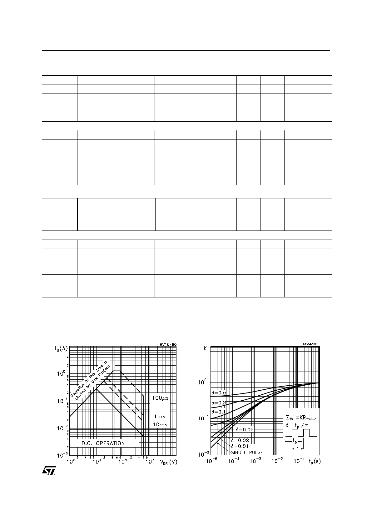
Thermal I mpedanceSafe Operating Area
3/9
Page 4

STQ1NC60R
Output Characteristics Transfer Characteristics
.
Tranconductance
Static Drain-Source On Resistance
Gate Charge vs Gate-source Voltage Capacitance Variations
4/9
Page 5

Source-drain Diode Forw ard Characteristics
STQ1NC60R
Normalized On Resistance vs TemperatureNormalized Ga te Thereshold Voltage vs Temp.
5/9
Page 6

STQ1NC60R
Fig. 2: Unclamped Inductive WaveformFig. 1: Unclamped Inductive Load Test Circuit
Fig. 3: Switching Times Test Circuit For
Resistive Load
Fig. 5: Test Circuit For Inductive Load Switching
And Diode Recovery Times
Fig. 4: Gate Charge tes t Circuit
6/9
Page 7

TO-92 MECHANICAL DATA
STQ1NC60R
DIM.
A 4.32 4.95 0.170 0.194
b 0.36 0.51 0.014 0.020
D 4.45 4.95 0.175 0.194
E 3.30 3.94 0.130 0.155
e 2.41 2.67 0.094 0.105
e1 1.14 1.40 0.044 0.055
L 12.70 15.49 0.50 0.610
R 2.16 2.41 0.085 0.094
S1 0.92 1.52 0.036 0.060
W 0.41 0.56 0.016 0.022
V5° 5°
MIN. TYP MAX. MIN. TYP. MAX.
mm. inch
7/9
Page 8

STQ1NC60R
TO-92 AMMOPACK
DIM.
A1 4.8 0.19
T 3.8 0.15
T1 1.6 0.06
T2 2.3 0.09
d 0.48 0.02
P0 12.5 12.7 12.9 0.49 0.5 0.51
P2 5.65 6.35 7.05 0.22 0.25 0.27
F1, F2 2.44 2.54 2.94 0.09 0.1 0.11
delta H -2 2 -0.08 0.08
W 17.5 18 19 0.69 0.71 0.74
W0 5.7 6 6.3 0.22 0.23 0.24
W1 8.5 9 9.25 0.33 0.35 0.36
W2 0.5 0.02
H 18.5 20.5 0.72 0.80
H0 15.5 16 16.5 0.61 0.63 0.65
H1 25 0.98
D0 3.8 4 4.2 0.15 0.157 0.16
t 0.9 0.035
L 11 0.43
l1 3 0.11
delta P -1 1 -0.04 0.04
MIN. TYP MAX. MIN. TYP. MAX.
mm. inch
8/9
Page 9

STQ1NC60R
Information furnished is believed to be accurate and reliable. However, STMicroelectronics assumes no responsibility for the
consequences of u se of such inf ormat ion nor for any in fring ement of p aten ts or othe r ri ghts of th ird p arties whic h may resul t f rom
its use. No license is granted by implication or otherwise under any patent or patent rights of STMicroelectronics. Specifications
mentioned in this publication are subject to change without notice. This publication supersedes and replaces all information
previously supplied. STMicroelectronics products are not authorized for use as critical components in life support devices or
systems without express written approval of STMicroelectronics.
Australia - Brazil - Canada - China - Finland - France - Germany - Hong Kong - India - Israel - Italy - Japan - Malaysia - Malta - Morocco
© The ST logo is a registered trademark of STMicroelectronics
© 2003 STMicroelectronics - Printed in Italy - All Rights Reserved
Singapore - Spain - Sweden - Switzerland - United Kingdom - United States.
STMicroelectronics GROUP OF COMPANIES
© http://www.st.com
9/9
 Loading...