

Page 1

MAINPRODUCT CHARACTERISTICS
STPS745D/F/G
POWER SCHOTTKY RECTIFIER
I
F(AV)
V
RRM
7.5 A
45 V
Tj (max) 175 °C
(max) 0.57 V
V
F
FEATURESAND BENEFITS
VERYSMALLCONDUCTIONLOSSES
NEGLIGIBLESWITCHINGLOSSES
EXTREMELYFAST SWITCHING
INSULATEDPACKAGE:ISOWATT220AC
Insulatingvoltage= 2000VDC
Capacitance= 12pF
DESCRIPTION
Single Schottky rectifier suited for Switch Mode
Power Supply and high frequencyDC to DC converters.
Packaged either in TO-220AC, ISOWATT220AC
2
or D
PAK, this device is intended for use in low
voltage, high frequency inverters, free wheeling
and polarityprotectionapplications.
ABSOLUTERATINGS
(limiting values)
TO-220AC
STPS745D
A
K
K
D2PAK
STPS745G
A
K
ISOWATT220AC
STPS745F
A
NC
Symbol Parameter Value Unit
V
RRM
I
F(RMS)
I
F(AV)
Repetitivepeakreversevoltage 45 V
RMSforwardcurrent 20 A
Averageforward current
δ
= 0.5
TO-220AC/
2
PAK
D
Tc = 160°C 7.5 A
ISOWATT220AC Tc = 145°C
I
FSM
Surgenonrepetitiveforward
tp = 10ms sinusoidal 150 A
current
I
RRM
I
RSM
Repetitivepeakreversecurrent tp = 2µs square F = 1kHz 1 A
Non repetitivepeak reverse
tp = 100 µs square 2 A
current
Tstg Storagetemperature range - 65 to+ 175 °C
Tj Maximum operatingjunction temperature* 175 °C
dV/dt Criticalrate of rise of reverse voltage 10000 V/µs
dPtot
*:
dTj
June 1999 - Ed: 4D
<
1
Rth(j−a
thermal runawayconditionfor a diode on its ownheatsink
)
1/7
Page 2
STPS745D/F/G
THERMALRESISTANCES
Symbol Parameter Value Unit
R
th (j-c)
Junctionto case TO-220AC/ D2PAK 3.0 °C/W
ISOWATT220AC 5.5
STATICELECTRICAL CHARACTERISTICS
Symbol Parameter TestsConditions Min. Typ. Max. Unit
* Reverseleakage current Tj = 25°CV
I
R
R=VRRM
100
Tj = 125°C 5 15 mA
* Forwardvoltagedrop Tj = 125°CI
V
F
Tj = 25°CI
Tj = 125°CI
Pulse test : * tp = 380 µs, δ <2%
= 7.5 A 0.5 0.57 V
F
= 15 A 0.84
F
= 15 A 0.65 0.72
F
To evaluatethe conductionlossesuse thefollowingequation:
P = 0.42x I
F(AV)
+0.020I
F2(RMS)
µ
A
2/7
Page 3
STPS745D/F/G
Fig. 1:
Average forward power dissipation versus
averageforwardcurrent.
PF(av)(W)
6
5
4
3
2
1
0
012345678910
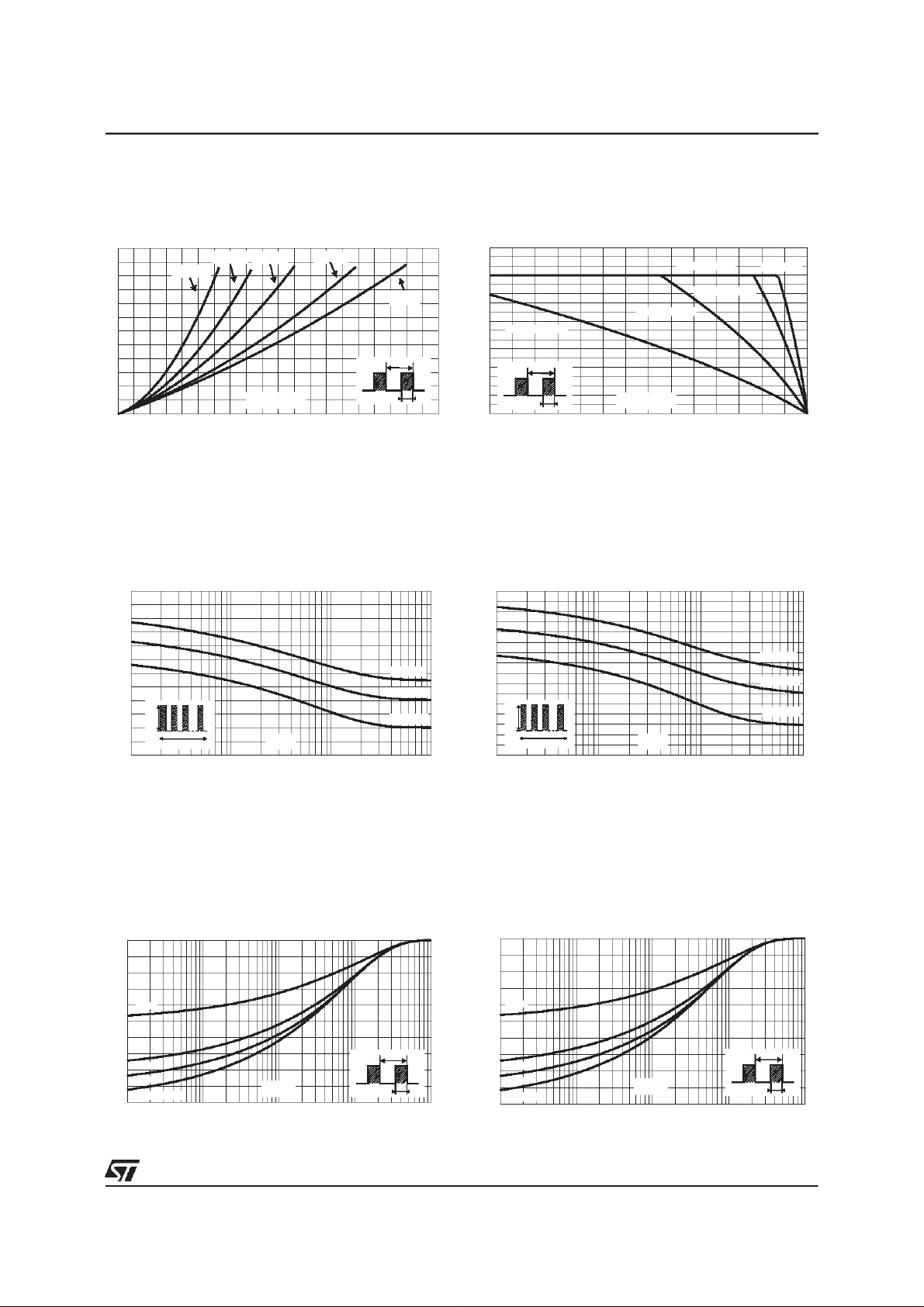
Fig. 3-1:
current versus overload duration (maximum
values) (TO-220ACand D
IM(A)
120
100
80
60
40
IM
20
0
1E-3 1E-2 1E-1 1E+0
δ = 0.1
δ = 0.05
IF(av)(A)
δ= 0.5δ = 0.2
δ =1
T
=tp/T tp
δ
Non repetitive surge peak forward
2
PAK).
Tc=50°C
Tc=100°C
Tc=150°C
δ=0.5
t
t(s)
Fig. 2:
Average current versus ambient
temperature (δ = 0.5).
IF(av)(A)
9
8
7
6
5
Rth(j-a)=Rth(j-c)
ISOWATT220AB
Rth(j-a)=15°C/W
Rth(j-a)=40°C/W
TO-220AC
4
3
2
1
0
0 25 50 75 100 125 150 175
Fig. 3-2:
δ
T
=tp/T
tp
Tamb(°C)
Non repetitive surge peak forward
current versus overload duration (maximum
values) (ISOWATT220AC).
IM(A)
80
70
60
50
40
30
20
IM
10
0
1E-3 1E-2 1E-1 1E+0
δ=0.5
t
t(s)
Tc=50°C
Tc=100°C
Tc=150°C
Fig. 4-1:
impedancejunction to caseversus pulse duration
(TO-220ACand D
Relative variation of thermal transient
2
PAK).
Zth(j-c)/Rth(j-c)
1.0
0.8
δ= 0.5
0.6
0.4
δ
=tp/T
T
tp
δ = 0.2
0.2
δ = 0.1
Single pulse
0.0
1E-4 1E-3 1E-2 1E-1 1E+0
tp(s)
Fig. 4-2:
Relative variation of thermal transient
impedancejunction to case versus pulse duration
(ISOWATT220AC).
Zth(j-c)/Rth(j-c)
1.0
0.8
δ = 0.5
0.6
0.4
δ
=tp/T
T
tp
3/7
δ = 0.2
0.2
δ = 0.1
Single pulse
0.0
1E-3 1E-2 1E-1 1E+0 1E+1
tp(s)
Page 4

STPS745D/F/G
Fig. 5:
Reverse leakage current versus reverse
voltageapplied(typical values).
IR(µA)
5E+4
1E+4
1E+3
1E+2
Tj=150°C
Tj=125°C
Tj=100°C
Tj=75°C
Tj=50°C
1E+1
Tj=25°C
1E+0
VR(V)
1E-1
0 5 10 15 20 25 30 35 40 45
Fig. 7: Forward voltage drop versus forward
current(maximum values).
IFM(A)
100.0
Tj=125°C
Typicalvalues
10.0
Tj=125°C
1.0
VFM(V)
0.1
0.0 0.2 0.4 0.6 0.8 1.0 1.2 1.4 1.6
Tj=25°C
Fig. 6:
Junction capacitance versus reverse
voltageapplied (typicalvalues).
C(pF)
1000
F=1MHz
Tj=25°C
500
200
VR(V)
100
12 51020 50
Fig. 8:
Thermal resistance junction to ambient
versus copper surface under tab (Epoxy printed
circuitboard,copper thickness:35µm).
Rth(j-a) (°C/W)
80
70
60
50
40
30
20
10
0
0 2 4 6 8 10 12 14 16 18 20
S(Cu)
(cm )
4/7
Page 5

PACKAGEMECHANICAL DATA
2
D
PAK(Plastic)
L2
E
L
L3
B2
B
G
* FLATZONE NO LESSTHAN 2mm
C2
A1
STPS745D/F/G
DIMENSIONS
REF.
A
A 4.40 4.60 0.173 0.181
A1 2.49 2.69 0.098 0.106
D
A2 0.03 0.23 0.001 0.009
B 0.70 0.93 0.027 0.037
B2 1.14 1.70 0.045 0.067
C 0.45 0.60 0.017 0.024
C
R
C2 1.23 1.36 0.048 0.054
D 8.95 9.35 0.352 0.368
E 10.00 10.40 0.393 0.409
A2
G 4.88 5.28 0.192 0.208
L 15.00 15.85 0.590 0.624
M
*
V2
L2 1.27 1.40 0.050 0.055
L3 1.40 1.75 0.055 0.069
M 2.40 3.20 0.094 0.126
R 0.40typ. 0.016typ.
V2 0° 8° 0° 8°
Millimeters Inches
Min. Max. Min. Max.
FOOTPRINT DIMENSIONS (in millimeters)
16.90
10.30
1.30
8.90
3.70
5.08
5/7
Page 6

STPS745D/F/G
PACKAGEMECHANICAL DATA
TO-220AC
H2
L5
ØI
L6
L2
L9
F1
L4
F
G
DIMENSIONS
REF.
Millimeters Inches
Min. Max. Min. Max.
A
C
L7
A 4.40 4.60 0.173 0.181
C 1.23 1.32 0.048 0.051
D 2.40 2.72 0.094 0.107
E 0.49 0.70 0.019 0.027
F 0.61 0.88 0.024 0.034
F1 1.14 1.70 0.044 0.066
D
G 4.95 5.15 0.194 0.202
H2 10.00 10.40 0.393 0.409
L2 16.40typ. 0.645typ.
M
E
L4 13.00 14.00 0.511 0.551
L5 2.65 2.95 0.104 0.116
L6 15.25 15.75 0.600 0.620
L7 6.20 6.60 0.244 0.259
L9 3.50 3.93 0.137 0.154
M 2.6 typ. 0.102typ.
Diam.I 3.75 3.85 0.147 0.151
6/7
Page 7

PACKAGEMECHANICAL DATA
ISOWATT220AC
STPS745D/F/G
H
A
B
REF.
Millimeters Inches
DIMENSIONS
Min. Typ. Max. Min. Typ. Max.
A 4.40 4.60 0.173 0.181
Diam
L6
L2
L3
L7
B 2.50 2.70 0.098 0.106
D 2.40 2.75 0.094 0.108
E 0.40 0.70 0.016 0.028
F 0.75 1.00 0.030 0.039
F1 1.15 1.70 0.045 0.067
F1
G 4.95 5.20 0.195 0.205
H 10.00 10.40 0.394 0.409
L2 16.00 0.630
L3 28.60 30.60 1.125 1.205
F
G
DE
L6 15.90 16.40 0.626 0.646
L7 9.00 9.30 0.354 0.366
Diam 3.00 3.20 0.118 0.126
Type Marking Package Weight Baseqty Delivery mode
STPS745D STPS745D TO-220AC 1.86g. 50 Tube
STPS745F STPS745F ISOWATT220AC 2 g. 50 Tube
2
STPS745G STPS745G D
STPS745G-TR STPS745G D
PAK 1.48g. 50 Tube
2
PAK 1.48g. 1000 Tape & reel
Coolingmethod:by conduction(C)
Recommendedtorquevalue:0.55 N.m
Maximumtorquevalue:0.7 N.m.
Epoxymeets UL94,V0
Informationfurnishedis believed to be accurate andreliable. However,STMicroelectronics assumes no responsibilityfor theconsequences of
use of such information nor forany infringementof patents or otherrights ofthirdparties which mayresult fromits use. No license is granted by
implication or otherwise under any patent or patent rights of STMicroelectronics. Specifications mentioned in this publication are subject to
change without notice.This publication supersedes andreplacesall information previously supplied.
STMicroelectronics products are not authorized for use as critical components in life support devices or systems without express written approval of STMicroelectronics.
The ST logo is a registered trademarkof STMicroelectronics
1999 STMicroelectronics - Printed inItaly - All rightsreserved.
STMicroelectronics GROUP OF COMPANIES
Australia -Brazil - China - Finland - France - Germany - Hong Kong - India - Italy - Japan - Malaysia
Malta - Morocco - Singapore - Spain - Sweden - Switzerland - United Kingdom - U.S.A.
http://www.st.com
7/7
 Loading...