

Page 1
MAINPRODUCTCHARACTERISTICS
STPS640CT/CF/CB
POWER SCHOTTKY RECTIFIER
I
F(AV)
V
RRM
2x3A
40 V
Tj (max) 150 °C
(max) 0.57 V
V
F
FEATURESAND BENEFITS
VERYSMALL CONDUCTIONLOSSES
NEGLIGIBLESWITCHINGLOSSES
EXTREMELYFASTSWITCHING
LOW FORWARDDROP VOLTAGE
LOW CAPACITANCE
LOW THERMAL RESISTANCE
INSULATEDPACKAGE:
Insulatingvoltage= 2000V DC
Capacitance= 12pF
SMD PACKAGE(tapeand reeloption: -TR)
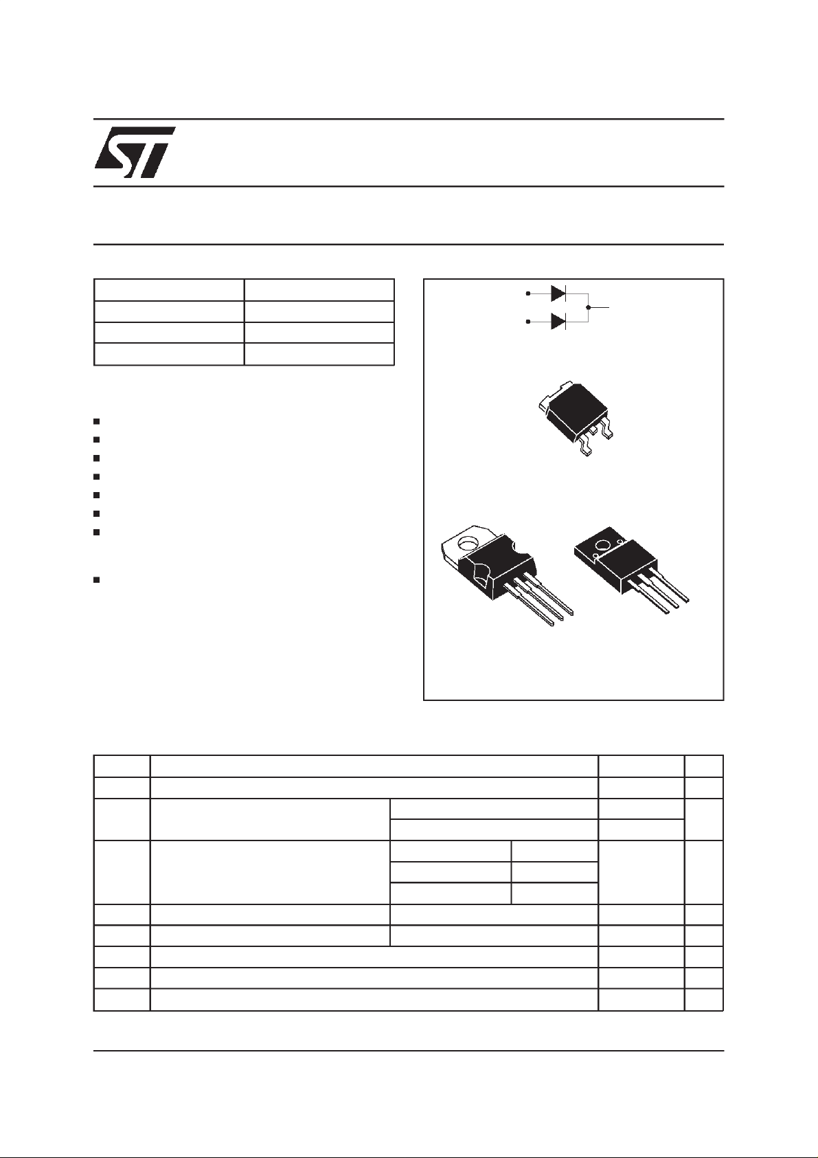
DESCRIPTION
Dual Schottky rectifier suited to Switch Mode
PowerSuppliesandotherPowerConverters.
This device is intendedfor use in low and medium
voltage operation, and particulary, in high frequency circuitries where low switching losses are
required(free wheeling and polarityprotection).
A1
A2
TO-220AB
STPS640CT
K
A1
DPAK
STPS640CB
A2
K
A1
ISOWATT220AB
STPS640CF
K
A2
A2
K
A1
ABSOLUTERATINGS(limitingvalues, per diode)
Symbol Parameter Value Unit
V
RRM
I
F(RMS)
Repetitivepeak reversevoltage 40 V
RMSforwardcurrent TO-220AB/ ISOWATT220AB 10 A
DPAK 6
I
F(AV)
Averageforwardcurrent δ = 0.5 TO-220AB Tc= 135°C3A
ISOWATT220AB Tc= 130°C
DPAK Tc= 120°C
I
FSM
I
RRM
T
Surgenon repetitive forwardcurrent tp= 10 ms Sinusoidal 75 A
Repetitivepeak reversecurrent tp= 2µs F= 1kHz square 1 A
Storagetemperaturerange - 65 to +150 °C
stg
Tj Maximumoperatingjunction temperature 150 °C
dV/dt Criticalrate of riseof reverse voltage 10000 V/µs
August 1999 - Ed: 4A
1/6
Page 2
STPS640CT/CF/CB
THERMALRESISTANCES
Symbol Parameter Value Unit
R
R
th (j-c)
th(c)
Junctionto case TO-220AB/DPAK Perdiode
Coupling TO-220AB 0.5 °C/W
Whenthe diodes 1 and2 areused simultaneously:
∆
Tj(diode1) = P(diode1)x R
(Perdiode) + P(diode2) x R
th(j-c)
Total
ISOWATT220AB Perdiode
Total
ISOWATT220AB 3
th(c)
5.5
3
7.5
5.2
°C/W
STATICELECTRICALCHARACTERISTICS
(per diode)
Symbol Tests Conditions Min. Typ. Max. Unit
* Reverseleakage current Tj = 25°CV
I
R
R=VRRM
100 µA
Tj = 125°C 2 10 mA
* Forwardvoltagedrop Tj = 25°CI
V
F
Tj = 25°CI
Tj = 125°CI
Tj = 125°CI
Pulse test : * tp = 380µs, δ <2%
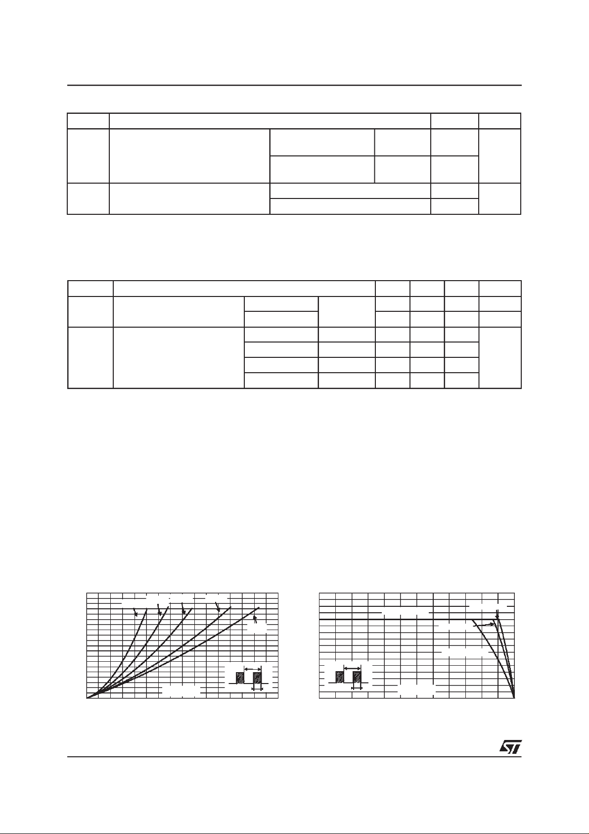
To evaluate the maximum conduction losses use the followingequation :
P = 0.42 x I
Fig. 1: Average forward power dissipationversus
averageforwardcurrent (per diode).
F(AV)
+0.050 I
F2(RMS)
Fig. 2: Averagecurrentversusambienttemperature
(δ= 0.5,per diode).
= 3 A 0.63 V
F
= 6 A 0.84
F
= 3 A 0.5 0.57
F
= 6 A 0.67 0.72
F
PF(av)(W)
2.50
2.25
2.00
1.75
1.50
1.25
1.00
0.75
0.50
0.25
0.00
0.0 0.5 1.0 1.5 2.0 2.5 3.0 3.5 4.0
δ = 0.05
δ = 0.1
δ = 0.2
IF(av) (A)
δ= 0.5
δ
=tp/T
2/6
δ =1
T
IF(av)(A)
4.0
3.5
3.0
2.5
2.0
1.5
1.0
tp
0.5
0.0
0 25 50 75 100 125 150
δ
T
=tp/T
tp
Rth(j-a)=Rth(j-c)
ISOWATT220AB
Tamb(°C)
TO-220AB/DPAK
Rth(j-a)=15°C/W
Page 3

STPS640CT/CF/CB
Fig. 3-1:
Nonrepetitivesurgepeakforwardcurrent
versusoverload duration.
(Maximum values,per diode)(TO-220AB/ DPAK).
IM(A)
45
40
35
30
25
20
15
IM
10
5
0
1E-3 1E-2 1E-1 1E+0
δ=0.5
t
t(s)
Tc=75°C
Tc=100°C
Tc=135°C
Fig. 4.1: Relative variation of thermal transient
impedancejunctionto case versuspulse duration
(TO-220AB/ DPAK).
Zth(j-c)/Rth(j-c)
1.0
Fig.3-2:
Nonrepetitivesurgepeakforwardcurrent
versusoverload duration.
(Maximum values,per diode)(ISOWATT220AB).
IM(A)
40
35
30
25
20
15
IM
10
5
0
1E-3 1E-2 1E-1 1E+0
δ=0.5
t
t(s)
Tc=75°C
Tc=100°C
Tc=130°C
Fig. 4-2: Relative variation of thermal transient
impedancejunctionto caseversus pulseduration
(ISOWATT220AB).
Zth(j-c)/Rth(j-c)
1.0
0.8
δ = 0.5
0.6
δ = 0.2
0.4
δ = 0.1
0.2
Single pulse
tp(s)
0.0
1E-3 1E-2 1E-1 1E+0
Fig. 5:
Reverse leakage current versus reverse
δ
=tp/T
T
tp
voltageapplied (typicalvalues, per diode).
IR(A)
1E-2
Tj=150°C
1E-3
1E-4
1E-5
0 5 10 15 20 25 30 35 40
Tj=125°C
Tj=100°C
Tj=75°C
VR(V)
0.8
δ = 0.5
0.6
0.4
δ = 0.2
δ = 0.1
0.2
0.0
Fig. 6:
Single pulse
1E-3 1E-2 1E-1 1E+0 1E+1
Junction capacitance versus reverse
tp(s)
T
=tp/T tp
δ
voltageapplied (typicalvalues,per diode).
C(pF)
500
100
10
12 51020 50
VR(V)
F=1MHz
Tj=25°C
3/6
Page 4

STPS640CT/CF/CB
Fig.7: Forwardvoltagedr opversusforwardcurr ent
(maximum values,per diode).
IFM(A)
10.0
Typicalvalues
Tj=150°C
1.0
0.1
0.0 0.1 0.2 0.3 0.4 0.5 0.6 0.7 0.8 0.9 1.0
Tj=125°C
VFM(V)
PACKAGEMECHANICALDATA
TO-220AB
A
C
D
M
L2
F1
H2
Dia
L5
L6
F2
L9
L4
F
G1
G
Fig.8: Thermalresistancejunctiontoambientversus
copper surface under tab (Epoxy printed circuit
board FR4, copperthickness:35µm).
Rth(j-a) (°C/W)
80
70
60
50
40
30
20
10
0
0 4 8 12 16 20 24 28 32 36 40
S(Cu)
(cm )
DIMENSIONS
REF.
Millimeters Inches
Min. Max. Min. Max.
A 4.40 4.60 0.173 0.181
C 1.23 1.32 0.048 0.051
D 2.40 2.72 0.094 0.107
E 0.49 0.70 0.019 0.027
L7
F 0.61 0.88 0.024 0.034
F1 1.14 1.70 0.044 0.066
F2 1.14 1.70 0.044 0.066
G 4.95 5.15 0.194 0.202
G1 2.40 2.70 0.094 0.106
H2 10 10.40 0.393 0.409
L2 16.4 typ. 0.645typ.
L4 13 14 0.511 0.551
L5 2.65 2.95 0.104 0.116
E
L6 15.25 15.75 0.600 0.620
L7 6.20 6.60 0.244 0.259
L9 3.50 3.93 0.137 0.154
M 2.6typ. 0.102typ.
Diam. 3.75 3.85 0.147 0.151
4/6
Page 5

PACKAGEMECHANICALDATA
DPAK
STPS640CT/CF/CB
DIMENSIONS
REF.
A 2.20 2.40 0.086 0.094
A1 0.90 1.10 0.035 0.043
A2 0.03 0.23 0.001 0.009
B 0.64 0.90 0.025 0.035
B2 5.20 5.40 0.204 0.212
C 0.45 0.60 0.017 0.023
C2 0.48 0.60 0.018 0.023
D 6.00 6.20 0.236 0.244
E 6.40 6.60 0.251 0.259
G 4.40 4.60 0.173 0.181
H 9.35 10.10 0.368 0.397
L2 0.80 typ. 0.031typ.
L4 0.60 1.00 0.023 0.039
V2 0° 8° 0° 8°
Millimeters Inches
Min. Max Min. Max.
FOOTPRINT DIMENSIONS
6.7
2.32.3
(in millimeters)
6.7
3
3
1.61.6
5/6
Page 6

STPS640CT/CF/CB
PACKAGE MECHANICAL DATA
ISOWATT220AB
DIMENSIONS
REF.
Millimeters Inches
Min. Max. Min. Max.
A 4.40 4.60 0.173 0.181
B 2.50 2.70 0.098 0.106
D 2.50 2.75 0.098 0.108
E 0.40 0.70 0.016 0.028
F 0.75 1.00 0.030 0.039
F1 1.15 1.70 0.045 0.067
F2 1.15 1.70 0.045 0.067
G 4.95 5.20 0.195 0.205
G1 2.40 2.70 0.094 0.106
H 10.00 10.40 0.394 0.409
L2 16.00typ. 0.630 typ.
L3 28.60 30.60 1.125 1.205
L4 9.80 10.60 0.386 0.417
L6 15.90 16.40 0.626 0.646
L7 9.00 9.30 0.354 0.366
Diam 3.00 3.20 0.118 0.126
Orderingtype Marking Package Weight Base qty Deliverymode
STPS640CT STPS640CT TO-220AB 2.20g 50 Tube
STPS640CB S640C DPAK 0.30g 75 Tube
STPS640CB-TR S640C DPAK 0.30g 2500 Tapeand reel
STPS640CF STPS640CF ISOWATT220AB 2.08g 50 Tube
Epoxymeets UL94,V0
Informationfurnished is believed to be accurate and reliable. However, STMicroelectronicsassumes no responsibility for the consequences of
use ofsuch informationnor forany infringementof patentsor other rightsof thirdparties which mayresult from its use. No license isgrantedby
implication or otherwise under any patent or patent rights of STMicroelectronics. Specifications mentioned in this publication are subject to
change without notice. This publication supersedes and replaces all information previously supplied.
STMicroelectronics products are not authorized for use as critical components in life support devices or systems without express written approval ofSTMicroelectronics.
The ST logo is a registeredtrademark ofSTMicroelectronics
1999 STMicroelectronics - Printed in Italy - All rights reserved.
STMicroelectronics GROUP OF COMPANIES
Australia - Brazil - China - Finland - France - Germany - Hong Kong- India- Italy- Japan- Malaysia
Malta - Morocco -Singapore - Spain - Sweden - Switzerland - United Kingdom - U.S.A.
http://www.st.com
6/6
 Loading...