

Page 1
®
STPS41L45CG/CT/CR
LOW DROP POWER SCHOTTKY RECTIFIER
MAIN PRODUCTS CHARACTERISTICS
I
F(AV)
V
RRM
2x20A
45 V
Tj (max) 150 °C
V
(max) 0.47 V
F
FEATURES AND BENEFITS
VERY SMALL CONDUCTION LOSSES
■
NEGLIGIBLE SWITCHING LOSSES
■
EXTREMELY FAST SWITCHING
■
LOW FORWARD VOLTAGE DROP
■
■ LOWTHERMAL RESISTANCE
■ AVALANCHECAPABILITY SPECIFIED
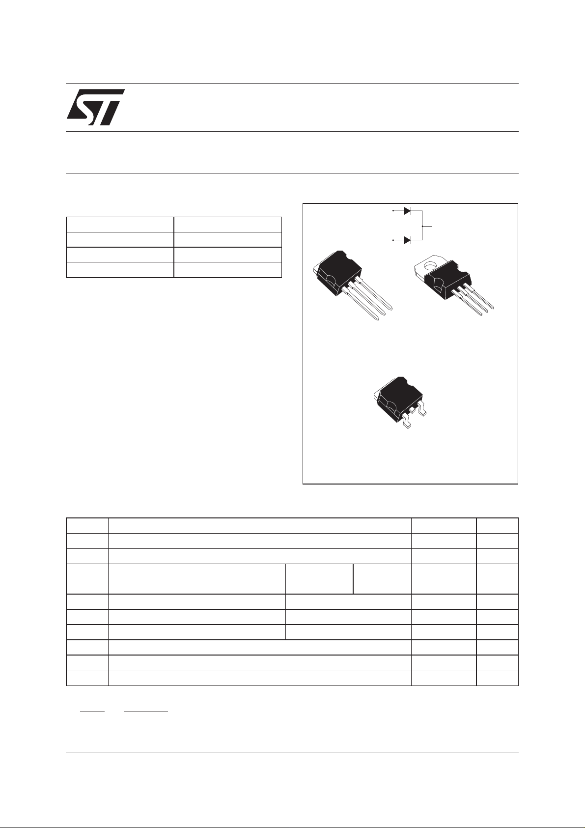
DESCRIPTION
Dual center tab Schottky rectifier suited for 5V
output in off line AC/DC power supplies.
Packaged in D2PAK, I2PAK and TO-220AB this
device is intended for use in low voltage, high
frequency inverters, free-wheeling and polarity
protection applications.
A1
A2
A1
2
PAK
I
STPS41L45CR
K
STPS41L45CG
A2
K
D2PAK
K
TO-220AB
STPS41L45CT
A2
A1
A1
A2
K
ABSOLUTE RATINGS (limiting values, per diode)
Symbol Parameter Value Unit
V
RRM
I
F(RMS)
I
F(AV)
I
FSM
I
RRM
P
ARM
T
stg
Tj
dV/dt
dPtot
*:
Repetitive peak reverse voltage
RMS forward current
Average forward current Tc = 130°C
Surge non repetitive forward current tp = 10 ms sinusoidal
Peak repetitive reverse current tp=2 µs square F=1kHz
Repetitive peak avalanche power tp = 1µs Tj = 25°C
Storage temperature range
Maximum operating junction temperature *
Critical rate of rise reverse voltage
<
dTj Rth j a
July 2003 - Ed : 3A
Per diode
δ = 0.5
Per device
thermal runaway condition for a diode on its own heatsink
−1()
45 V
30 A
20
40
220 A
1A
10000 W
-65 to+175 °C
150 °C
10000 V/µs
A
1/6
Page 2
STPS41L45CG / STPS41L45CT / STPS41L45CR
THERMAL RESISTANCES
Symbol Parameter Value Unit
R
th(j-c)
R
th(c)
Junction to case
Coupling
When the diodes 1 and 2 are used simultaneously :
∆ Tj(diode 1) = P(diode1) x R
(Per diode) + P(diode 2) x R
th(j-c)
STATIC ELECTRICAL CHARACTERISTICS (per diode)
Symbol Parameter Tests Conditions Min. Typ. Max. Unit
Per diode
Total
th(c)
1.5
0.8
0.1
°C/W
*
I
R
Reverse leakage current Tj = 25°C V
R=VRRM
Tj = 125°C
V
*
F
Forward voltage drop Tj = 25°CI
Tj = 125°C I
Tj=25°CI
Tj = 125°C I
=20A
F
=20A
F
=40A
F
=40A
F
Pulse test : * tp = 380 µs, δ <2%
To evaluate the conduction losses use the following equation :
P=0.28xI
Fig.1:Conductionlossesversus average current.
F(AV)
+ 0.0095 I
F2(RMS)
Fig. 2: Average forward current versus ambient
temperature (δ = 0.5).
1.2 mA
110 220 mA
0.53 V
0.42 0.47
0.68
0.60 0.66
PF(av)(W)
14
12
10
8
6
4
2
0
0 2 4 6 8 10121416182022242628
δ = 0.05
δ = 0.1
δ = 0.2
IF(av)(A)
δ = 0.5
δ
δ = 1
T
=tp/T
2/6
IF(av)(A)
25
20
15
10
5
tp
0
T
tp
=tp/T
δ
0 25 50 75 100 125 150
Rth(j-a)=Rth(j-c)
Rth(j-a)=50°C/W
Tamb(°C)
Page 3

STPS41L45CG / STPS41L45CT / STPS41L45CR
Fig. 3: Normalized avalanche power derating
versus pulse duration.
P(t)
ARM p
P (1µs)
ARM
1
0.1
0.01
t (µs)
0.001
0.10.01 1
p
10 100 1000
Fig. 5: Non repetitive surge peak forward current
versus overload duration (maximum values).
IM(A)
220
200
180
160
140
120
100
80
60
IM
40
20
0
1.E-03 1.E-02 1.E-01 1.E+00
δ=0.5
t
t(s)
Tc=25°C
Tc=75°C
Tc=125°C
Fig. 4: Normalized avalanche power derating
versus junction temperature.
P(t)
ARM p
P (25°C)
ARM
1.2
1
0.8
0.6
0.4
0.2
T (°C)
0
j
0 25 50 75 100 125 150
Fig. 6: Relative variation of thermal impedance
junction to case versus pulse duration.
Zth(j-c)/Rth(j-c)
1.0
0.9
0.8
0.7
δ = 0.5
0.6
0.5
0.4
δ = 0.2
δ = 0.1
0.3
0.2
Single pulse
0.1
0.0
1.E-03 1.E-02 1.E-01 1.E+00
tp(s)
δ
=tp/T
T
tp
Fig. 7: Reverse leakage current versus reverse
voltage applied (typical values).
IR(mA)
1.E+03
Tj=150°C
1.E+02
1.E+01
1.E+00
1.E-01
1.E-02
0 5 10 15 20 25 30 35 40 45
Tj=125°C
Tj=100°C
Tj=75°C
Tj=50°C
Tj=25°C
VR(V)
Fig. 8: Junction capacitance versus reverse voltage
applied (typical values).
C(nF)
10.0
1.0
VR(V)
0.1
1 10 100
F=1MHz
Vosc=30mV
Tj=25°C
3/6
Page 4

STPS41L45CG / STPS41L45CT / STPS41L45CR
Fig.9: Forward voltagedrop versus forwardcurrent.
IFM(A)
100
Tj=125°C
Tj=125°C
(Maximum values)
(Maximum values)
Tj=125°C
Tj=125°C
(Typical values)
10
PACKAGE MECHANICAL DATA
D
(Typical values)
Tj=25°C
(Maximum values)
1
0.0 0.1 0.2 0.3 0.4 0.5 0.6 0.7 0.8 0.9 1.0
2
PAK
L2
L
L3
E
G
VFM(V)
A
C2
A1
B2
B
* FLAT ZONE NO LESS THAN 2mm
C
A2
M
*
R
V2
D
Fig. 10: Thermal resistance junction to ambient versus copper surface under tab (epoxy printed board
FR4, Cu = 35µm) (STPS41L45CG only).
Rth(j-a)(°C/W)
80
70
60
50
40
30
20
10
0
0 5 10 15 20 25 30 35 40
S(cm²)
DIMENSIONS
REF.
Millimeters Inches
Min. Max. Min. Max.
A 4.40 4.60 0.173 0.181
A1 2.49 2.69 0.098 0.106
A2 0.03 0.23 0.001 0.009
B 0.70 0.93 0.027 0.037
B2 1.14 1.70 0.045 0.067
C 0.45 0.60 0.017 0.024
C2 1.23 1.36 0.048 0.054
D 8.95 9.35 0.352 0.368
E 10.00 10.40 0.393 0.409
G 4.88 5.28 0.192 0.208
L 15.00 15.85 0.590 0.624
L2 1.27 1.40 0.050 0.055
L3 1.40 1.75 0.055 0.069
M 2.40 3.20 0.094 0.126
R 0.40 typ. 0.016 typ.
V2 0° 8° 0° 8°
FOOTPRINT (dimensions in mm)
16.90
10.30
8.90
4/6
3.70
5.08
1.30
Page 5

PACKAGE MECHANICAL DATA
2
PAK
I
E
L2
L1
L
e
b2
b1
b
c2
D
A1
STPS41L45CG / STPS41L45CT / STPS41L45CR
DIMENSIONS
REF.
A
A 4.40 4.60 0.173 0.181
A1 2.49 2.69 0.098 0.106
b 0.70 0.93 0.028 0.037
b1 1.14 1.17 0.044 0.046
b2 1.14 1.17 0.044 0.046
c 0.45 0.60 0.018 0.024
c2 1.23 1.36 0.048 0.054
D 8.95 9.35 0.352 0.368
e 2.40 2.70 0.094 0.106
E 10.0 10.4 0.394 0.409
L 13.1 13.6 0.516 0.535
c
L1 3.48 3.78 0.137 0.149
L2 1.27 1.40 0.050 0.055
Millimeters Inches
Min. Max. Min. Max.
5/6
Page 6

STPS41L45CG / STPS41L45CT / STPS41L45CR
PACKAGE MECHANICAL DATA
TO-220AB
A
C
L7
D
M
E
L2
F2
F1
H2
Dia
L5
L6
L9
L4
F
G1
G
DIMENSIONS
REF.
Millimeters Inches
Min. Max. Min. Max.
A 4.40 4.60 0.173 0.181
C 1.23 1.32 0.048 0.051
D 2.40 2.72 0.094 0.107
E 0.49 0.70 0.019 0.027
F 0.61 0.88 0.024 0.034
F1 1.14 1.70 0.044 0.066
F2 1.14 1.70 0.044 0.066
G 4.95 5.15 0.194 0.202
G1 2.40 2.70 0.094 0.106
H2 10 10.40 0.393 0.409
L2 16.4 typ. 0.645 typ.
L4 13 14 0.511 0.551
L5 2.65 2.95 0.104 0.116
L6 15.25 15.75 0.600 0.620
L7 6.20 6.60 0.244 0.259
L9 3.50 3.93 0.137 0.154
M 2.6 typ. 0.102 typ.
Diam. 3.75 3.85 0.147 0.151
Ordering type
STPS41L45CG
Marking
STPS41L45CG
STPS41L45CG-TR STPS41L45CG D
Package Weight Base qty Delivery mode
2
D
PAK 1.48 g 50 Tube
2
PAK 1.48 g 1000 Tape & reel
STPS41L45CT STPS41L45CT TO-220AB 2.20 g 50 Tube
STPS41L45CR STPS41L45CR I
■
EPOXY MEETS UL94,V0
Informationfurnishedis believed to be accurate and reliable. However, STMicroelectronics assumes no responsibilityforthe consequences of
useof such information nor for any infringement of patentsor other rights of third parties which mayresultfrom its use. No license is granted by
implication or otherwise under any patent or patent rights of STMicroelectronics. Specifications mentioned in this publication are subject to
change without notice. This publication supersedes and replaces all information previously supplied.
STMicroelectronics products are not authorized for use as critical components in life support devices or systems without express written
approval of STMicroelectronics.
The ST logo is a registered trademark of STMicroelectronics
© 2003 STMicroelectronics - Printed in Italy - All rights reserved.
STMicroelectronics GROUP OF COMPANIES
Australia - Brazil - Canada - China - Finland - France - Germany
Hong Kong - India - Israel - Italy - Japan - Malaysia - Malta - Morocco - Singapore
Spain - Sweden - Switzerland - United Kingdom - United States.
6/6
2
PAK 1.49 g 50 Tube
http://www.st.com
 Loading...