

Page 1
®
LOW DROP OR-ing POW ER SCHOTTKY DIOD E
MAJOR PRODUCT CHARACTE RISTICS
I
F(AV)
V
RRM
Tj (max) 150°C
V
(max) 0.33 V
F
FEATURES AND BENEFITS
VERY LOW F O RWARD VO LTAGE DROP FOR
LESS POWER DISSIPATION AND REDUCED
HEATSINK SIZE
REVERSE VOLTAGE SUITED TO OR-ing OF
3V, 5V and 12V RA ILS
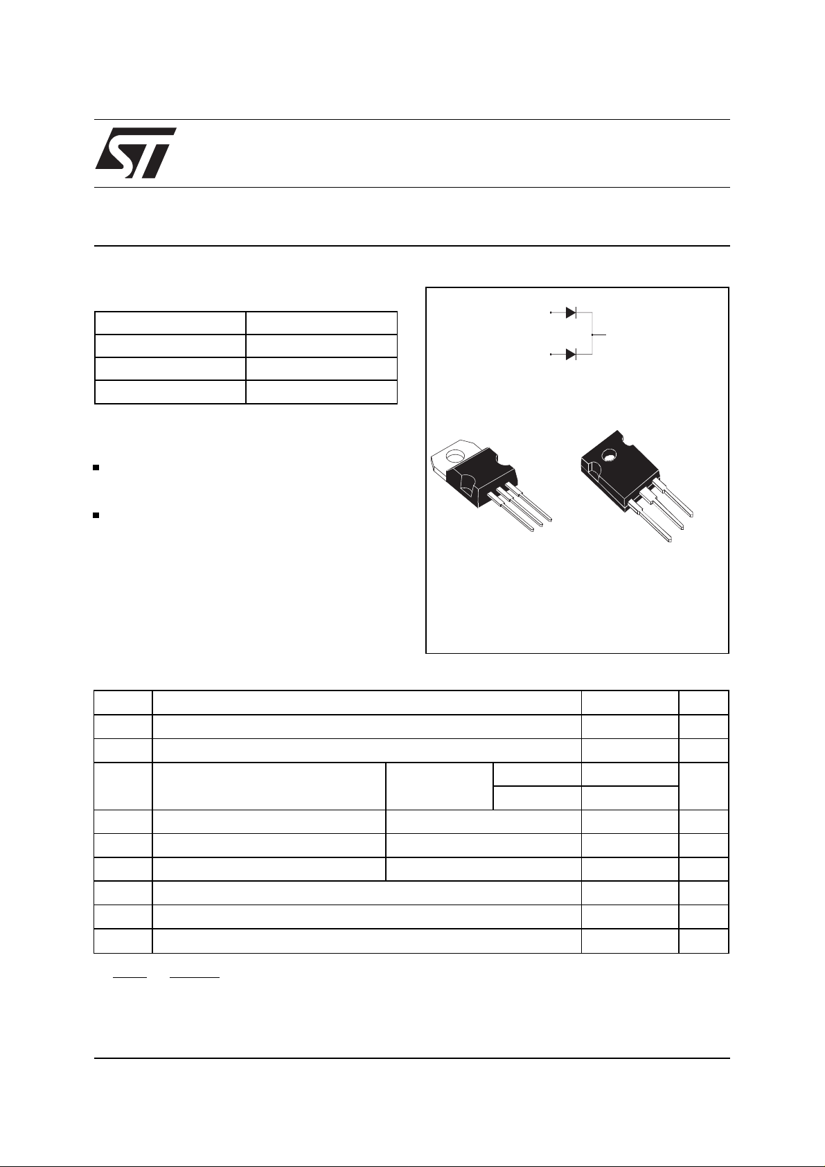
DESCR IPT ION
2 x 20 A
15 V
STPS40L15CW/CT
A1
K
A2
A2
K
A1
A1
A2
K
Dual center tap schottky rectifier packaged in
TO-220AB and TO-247, this device is especially
intended for use as OR-ing diode in fault tolerant
TO-220AB
STPS40L15CT
TO-247
STPS40L15CW
power supply equipments.
ABSOLUTE RATINGS (limiting values, per diode)
Symbol Parameter Value Unit
V
RRM
I
F(RMS)
I
F(AV)
I
FSM
I
RRM
I
RSM
T
stg
T
j
dV/dt
dPtot
* :
dTj
Repetitive peak reverse voltage
RMS forward current
Average forward current Tcase = 140°C
δ = 1
Surge non repetitive forward current tp = 10 ms Sinusoidal
Peak repetitive reverse current tp = 2 µs F = 1kHz
Non repetitive peak reverse current tp = 100 µs
Storage temperature range
Maximum operating junction temperature *
Critical rate of rise of reverse voltage
<
1
Rth(j−a
thermal runaway condition for a diode on its own heatsink
)
Total
Per diode
15 V
30 A
40 A
20
310 A
2A
3A
- 65 to + 150 °C
150 °C
10000 V/µs
November 1999 - Ed: 4A
1/5
Page 2
STPS40L15CW/CT
THERMA L RE SISTA NC ES
Symbol Parameter Value Unit
(j-c)
R
R
th
th (c)
Junction to case
STATIC ELECTRICAL CHARACTE RISTICS (Per diode)
Symbol Parameter Tests Conditions Min. Typ. Max. Unit
Per diode 1.6 °C/W
Total 0.85
Coupling 0.1 °C/W
*
I
R
V
F
Reverse leakage
current
*
Forward voltage drop Tj = 25°CI
Tj = 25°CV
Tj = 100°C
Tj = 25°CI
Tj = 125°C I
= V
R
= 19 A
F
= 40 A
F
= 19 A
F
Tj = 125°C IF = 40 A
Pulse test : * tp = 380 µs, δ < 2%
To evaluate the conduction losses use the following equation :
P = 0.18 x I
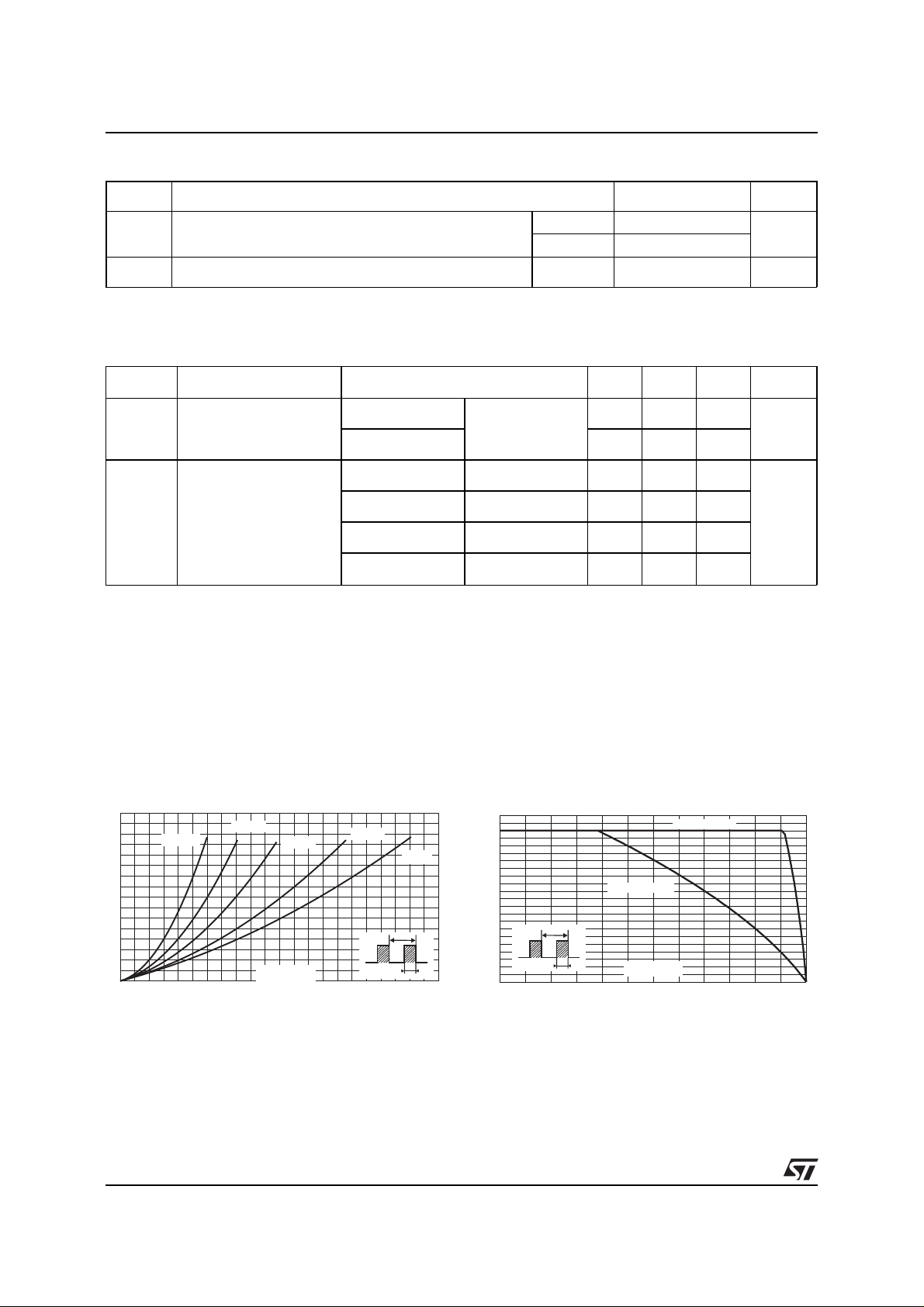
Fig. 1: Average forward power dis sipation versus
average forward current (per diode).
PF(av)(W)
8
7
6
5
4
3
2
1
0
0 2 4 6 8 10121416182022
δ = 0.05
F(AV)
+ 0.008 I
δ = 0.1
IF(av) (A)
F2(RMS )
δ = 0.2
δ = 0.5
δ
=tp/T
T
δ = 1
Fig. 2: Average forward current versus ambient
temperature (δ=1, per diode).
IF(av)(A)
22
20
18
16
14
12
10
8
6
4
tp
2
0
0 25 50 75 100 125 150
RRM
=tp/T
δ
6mA
200 500
0.41 V
0.52
0.28 0.33
0.42 0.50
Rth(j-a)=Rth(j-c)
Rth(j-a)=15°C/W
T
tp
Tamb(°C)
2/5
Page 3

STPS40L15CW/CT
Fig. 3: Non repetitive surge peak forward current
versus overload duration (maximum values per
diode).
IM(A)
250
200
150
100
I
M
50
0
1E-3 1E-2 1E-1 1E+0
t
δ
=0.5
t(s)
Tc=50°C
Tc=75°C
Tc=110°C
Fig. 5: Reverse leakage current versus reverse
voltage applied (typical values per diode) .
IR(mA)
5E+2
1E+2
Tj=100°C
Fig. 4: Relative variation of thermal impedance
junction to case versus pulse duration (per diode).
Zth(j-c)/Rth(j-c)
1.0
0.8
δ = 0.5
0.6
0.4
δ = 0.2
δ = 0.1
0.2
0.0
1.0E-4 1.0E-3 1.0E-2 1.0E-1 1.0E+0
Single pulse
tp (s)
δ
=tp/T
T
tp
Fig. 6: Junction capacitance versus reverse
voltage applied (typical values per diode).
C(nF)
5.0
F=1MHz
Tj=25°C
1E+1
1E+0
1E-1
0246810121416
Tj=25°C
VR(V)
Fig. 7: Forward voltage drop versus forward
current (typical values per diode) .
IFM(A)
200.0
100.0
10.0
Tj=150°C
Tj=25°C
Tj=125°C
Tj=75°C
1.0
VFM(V)
0.1
0.0 0.2 0.4 0.6 0.8 1.0 1.2 1.4 1.6
1.0
VR(V)
0.1
12 51020
Fig. 8: Forward voltage drop versus forward
current (typical maximum per diode).
IFM(A)
200
Tj=100°C
100
10
1
0 0.2 0.4 0.6 0.8 1 1.2 1.4 1.6 1.8
VFM(V)
3/5
Page 4

STPS40L15CW/CT
PACKAGE MECHANICAL DAT A
TO-220AB
REF.
DIMENSIONS
Millimeters Inches
H2
Dia
L5
L6
L2
F2
F1
F
G1
G
L9
L4
Cooling method: C
Recommended torque value: 0.55 m.N
Maximum torque value: 0.70 m.N
A
C
L7
A 4.40 4.60 0.173 0.181
C 1.23 1.32 0.048 0.051
D 2.40 2.72 0.094 0.107
E 0.49 0.70 0.019 0.027
F 0.61 0.88 0.024 0.034
F1 1.14 1.70 0.044 0.066
F2 1.14 1.70 0.044 0.066
Min. Max. Min. Max.
D
G 4.95 5.15 0.194 0.202
G1 2.40 2.70 0.094 0.106
H2 10 10.40 0.393 0.409
L2 16.4 typ. 0.645 typ.
M
E
L4 13 14 0.511 0.551
L5 2.65 2.95 0.104 0.116
L6 15.25 15.75 0.600 0.620
L7 6.20 6.60 0.244 0.259
L9 3.50 3.93 0.137 0.154
M 2.6 typ. 0.102 typ.
Diam. 3.75 3.85 0.147 0.151
4/5
Page 5

PACKAGE MECHANICAL DAT A
TO-247
V
V
H
L5
L
F2
F4
L1
F3
L3
F1
V2
F(x3)
G
= =
Dia.
L4L2
D
ME
A
STPS40L15CW/CT
DIMENSIONS
REF.
A 4.85 5.15 0.191 0.203
D 2.20 2.60 0.086 0.102
E 0.40 0.80 0.015 0.031
F 1.00 1.40 0.039 0.055
F1 3.00 0.118
F2 2.00 0.078
F3 2. 00 2.40 0.078 0.094
F4 3. 00 3.40 0.118 0.133
G 10.90 0.429
H 15.45 15.75 0.608 0.620
L 19.85 20.15 0.781 0.793
L1 3.70 4.30 0.145 0.169
L2 18.50 0.728
L3 14.20 14.80 0.559 0.582
L4 34.60 1.362
L5 5.50 0.216
M 2.00 3.00 0.078 0.118
V5° 5°
V2 60° 60°
Dia. 3.55 3.65 0.139 0.143
Millimeters Inches
Min. Typ. Max. Min. Typ. Max.
Cooling method: C
Recommended torque value: 0.8 m.N
Maximum torque value: 1.0 m.N
Ordering type Marking Package Weight Base qty Delivery mode
STPS40L15CW STPS40L15CW TO-247 4.4 g. 30 Tube
STPS40L15CT STPS40L15CT TO-220AB 2g 50 Tube
Epoxy meets UL94,V0
Information furnished is believed to be accurate and reliable. However, STMicroelectronics assumes no responsibility for the consequences of
use of such information nor for any infringement of patents or other rights of third parties which may result from its use. No license is granted by
implication or otherwi se un der any pat ent or patent rights of STMic roelec tronics. S pecifications ment ioned in t his publ ication are subject to
change without notice. This publication supersedes and replaces all information previously supplied.
STMicroelectronics products are not authorized for use as critical components in li fe s upport devices or systems wi thout express writte n approval of STMicroelectronics.
The ST logo is a registered trademark of STMicroe lectronics
© 1999 STMicroelectronics - Printed in Italy - All rights reser ved.
STMicroelectronics GROUP OF COMPANIES
Australia - Brazil - China - Finland - France - Germany - Hong Kong - India - Italy - Japan - Malaysia
Malta - Morocco - Singapore - Spain - Sweden - Switzerland - United Kingdom - U.S.A.
http://www.st.com
5/5
 Loading...