

Page 1
MAINPRODUCTCHARACTERISTICS
STPS140Z
POWER SCHOTTKY RECTIFIER
I
F
V
RRM
V
(max) 0.49 V
F
1A
40 V
Tj (max) 150°C
FEATURESAND BENEFITS
VERYSMALL CONDUCTION LOSSES
NEGLIGIBLESWITCHING LOSSES
EXTREMELYFASTSWITCHING
DESCRIPTION
Single Schottky rectifier suited for Switchmode
PowerSuppliesand highfrequencyDCto DC converters.
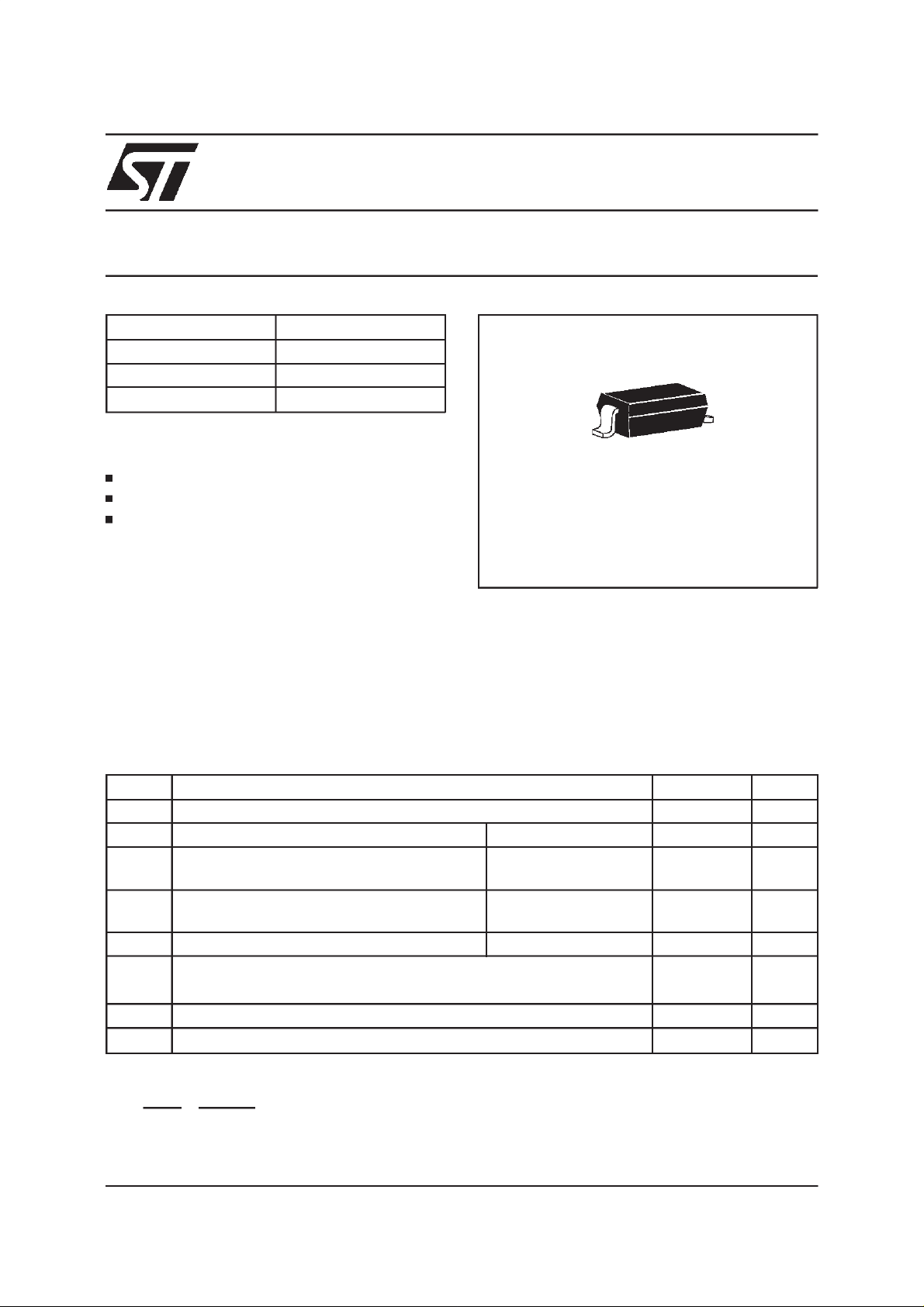
Packaged in SOD123, this device is intended for
use in low voltage, high frequency inverters, free
wheelingand polarity protection applications.Due
tothesmallsizeofthe packagethis devicefit GSM
andPCMCIA requirements.
ABSOLUTE RATINGS(limitingvalues)
SOD123
Symbol Parameter Value Unit
V
RRM
I
I
FSM
Repetitivepeak reversevoltage 40 V
Continuousforwardcurrent
F
T
=60°C1A
amb
Surgenon repetitiveforwardcurrent tp = 10 ms
5.5 A
Sinusoidal
I
RRM
Repetitivepeak reversecurrent tp = 2 µs square
0.5 A
F = 1kHz
I
RSM
T
stg
Nonrepetitive peak reversecurrent tp = 100µs square 1 A
Storagetemperaturerange - 65 to + 150 °C
Tj Maximumoperatingjunction temperature* 150
T
Maximumtemperaturefor solderingduring 10s 260 °C
L
dV/dt Criticalrate of riseof reverse voltage 10000 V/µs
dPtot
*
dTj
May 1999 - Ed:1
<
Rth(j−a
1
Thermal runawaycondition fora diode onits own heatsink.
)
1/5
Page 2
STPS140Z
THERMALRESISTANCES
Symbol Parameter Value Unit
R
th (j-a)
* with 50 mm2copper area (e=35µm)
Junctionto ambient* 175 °C/W
STATICELECTRICALCHARACTERISTICS
Symbol Tests Conditions TestsConditions Min. Typ. Max. Unit
* Reverse leakage current Tj = 25°CV
I
R
Tj = 25°CV
=5V 10 µA
R
=40V 40 µA
R
Tj = 100°C 1.5 5 mA
** Forwardvoltagedrop Tj = 25°CI
V
F
= 1 A 0.55 V
F
Tj = 100°C 0.45 0.51
Pulse test : * tp = 5 ms, δ <2%
** tp = 380µs, δ <2%
To evaluatethe maximum conductionlossesuse thefollowing equation:
P = 0.2 x I
F(AV)
+ 0.3 x I
F2(RMS)
atTj = 150°C
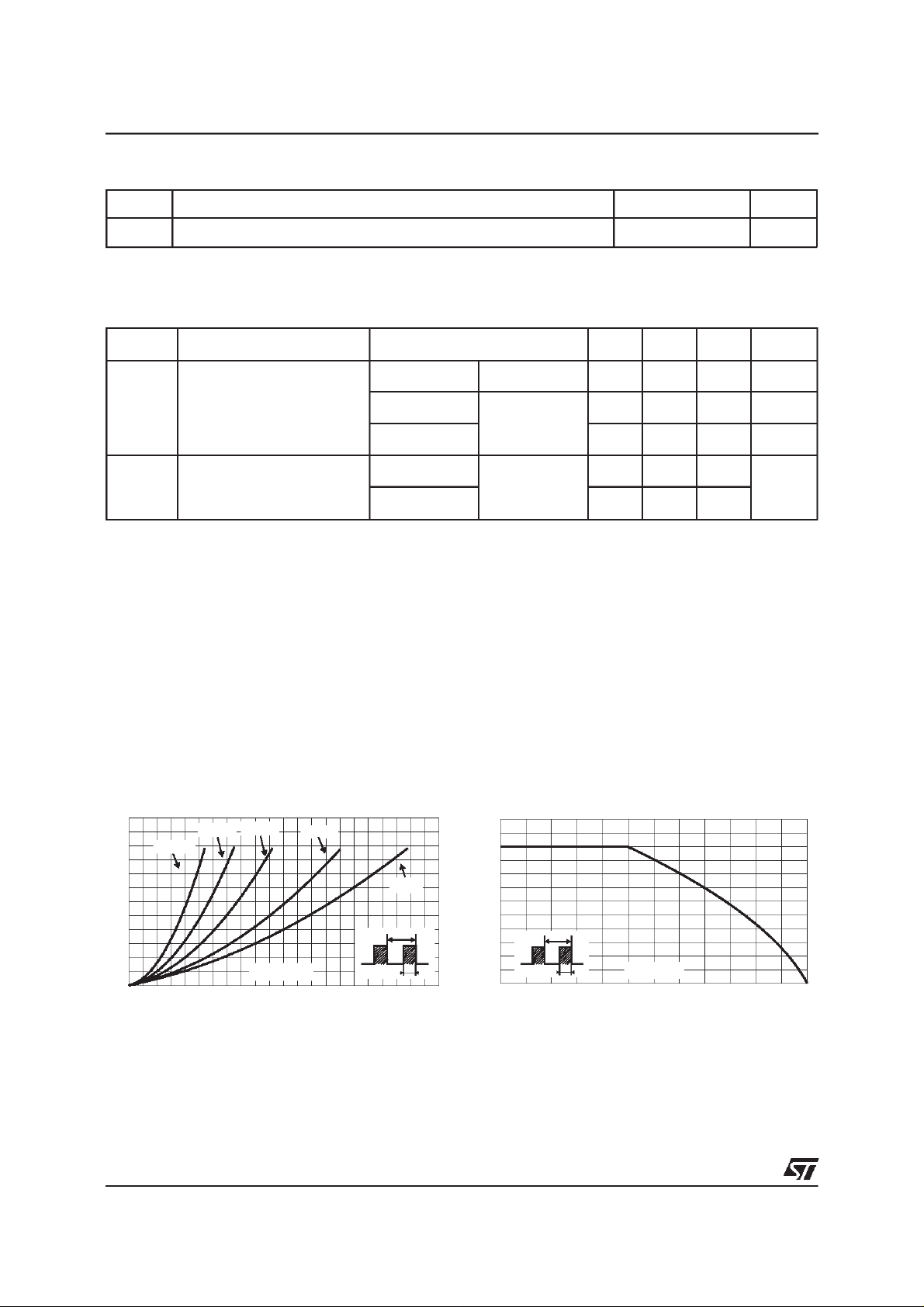
Fig. 1: Average forward power dissipationversus
averageforwardcurrent.
PF(av)(W)
0.6
0.5
0.4
0.3
0.2
0.1
0.0
δ = 0.05
0.0 0.1 0.2 0.3 0.4 0.5 0.6 0.7 0.8 0.9 1.0 1.1
2/5
δ = 0.1
δ = 0.2
IF(av)(A)
δ= 0.5
δ
=tp/T
δ =1
T
tp
Fig. 2: Average forward current versus ambient
temperature(δ=1).
IF(av)(A)
1.2
1.0
0.8
0.6
0.4
0.2
0.0
0 25 50 75 100 125 150
δ
=tp/T
T
tp
Tamb(°C)
Page 3

STPS140Z
Fig. 3:
Non repetive surge peak forward current
versusover l oaddur ati on(maxim umvalues) .
IM(A)
5
4
3
2
IM
1
0
1E-3 1E-2 1E-1 1E+0
Fig. 5:
δ=0.5
t
t(s)
Reverse leakage current versus reverse
Ta=25°C
Ta=60°C
voltageapplied (typicalvalue).
IR(mA)
5E+1
1E+1
1E+0
1E-1
1E-2
1E-3
1E-4
0 5 10 15 20 25 30 35 40
Tj=150°C
Tj=100°C
Tj=70°C
Tj=25°C
VR(V)
Fig.4:
Relativevariationofthermalimpedancejunction
to ambientversus pulse duration (epoxy printedcircuit
boardFR4withrecommendedpadlayout).
Zth(j-a)/Rth(j-a)
1E+0
δ= 0.5
δ = 0.2
δ= 0.1
1E-1
T
Single pulse
1E-2
tp(s)
1E-2 1E-1 1E+0 1E+1 5E+1
Fig. 6:
Reverse leakage current versus junction
δ
=tp/T
tp
temperature(typicalvalue).
IR[Tj] / IR[Tj=25°C]
5E+3
1E+3
1E+2
1E+1
1E+0
1E-1
VR=40V
Tj(°C)
0 25 50 75 100 125 150
Fig. 7: Junction capacitance versus reverse
voltageapplied (typicalvalue).
C(pF)
200
100
50
20
VR(V)
10
12 51020 50
F=1MHz
Tj=25°C
3/5
Page 4

STPS140Z
Fig. 8-1:
Forward voltage drop versus forward
current(high level, maximumvalues).
IFM(A)
5E+0
1E+0
1E-1
Tj=150°C
Tj=25°C
Tj=100°C
VFM(V)
1E-2
0.0 0.1 0.2 0.3 0.4 0.5 0.6 0.7 0.8 0.9 1.0 1.1 1.2
Fig. 9:
Thermal resistance junction to ambient
versuscoppe r surface(epoxy printed circuit board
FR4,copper thickness:35µm).
Fig. 8-2:
Forward voltage drop versus forward
current(low level,maximum values).
IFM(A)
2.0
1.8
1.6
1.4
1.2
1.0
0.8
0.6
Tj=150°C
0.4
0.2
0.0
0.0 0.1 0.2 0.3 0.4 0.5 0.6 0.7 0.8 0.9 1.0
VFM(V)
Tj=25°C
Tj=100°C
Rth(j-a) (°C/W)
300
280
260
240
220
200
180
160
140
120
100
0 102030405060708090100
S(Cu) (mm )
IF=1A
4/5
Page 5

PACKAGEMECHANICAL DATA
SOD123Plastic
H
b
E
D
c
G
A2
STPS140Z
DIMENSIONS
REF.
A1
A 1.45 0.057
A1 0 0.1 0 0.004
A2 0.85 1.35 0.033 0.053
A
b 0.55 Typ. 0.022 Typ.
c 0.15 Typ. 0.039 Typ.
D 2.55 2.85 0.1 0.112
E 1.4 1.7 0.055 0.067
G 0.25 0.01
H 3.55 3.95 0.14 0.156
Millimeters Inches
Min. Max. Min. Max.
Informationfurnishedis believed to be accurate and reliable. However, STMicroelectronics assumes no responsibility for the consequences of
use of such informationnor forany infringementofpatents or otherrights of third parties which may result fromitsuse.No license is grantedby
implication or otherwise under any patent or patent rights of STMicroelectronics. Specifications mentioned in this publication are subject to
change without notice.This publication supersedes and replaces all information previously supplied.
STMicroelectronics products are not authorized for use as critical components in life support devices or systemswithout express writtenapproval of STMicroelectronics.
The ST logo is a registeredtrademark ofSTMicroelectronics
1999 STMicroelectronics - Printed in Italy - All rights reserved.
STMicroelectronics GROUP OF COMPANIES
Australia - Brazil - China - Finland - France - Germany - Hong Kong- India- Italy- Japan- Malaysia
Malta - Morocco - Singapore - Spain - Sweden - Switzerland - United Kingdom - U.S.A.
http://www.st.com
5/5
 Loading...