

Page 1
®
MAIN PRODUCT CHARACTERISTIC S
STPS140A/U
POWER SCHO TTKY REC TIFIER
I
F(AV)
V
RRM
(max) 0.5 V
V
F
1 A
40 V
FEATURES AND BENEFITS
VERY SMALL CONDUCTION LOS SES
NEGLIGIBLE SWITCHING LOSS ES
LOW FORWARD VOLTA GE DROP
SURFACE MOUNTED DE VICE
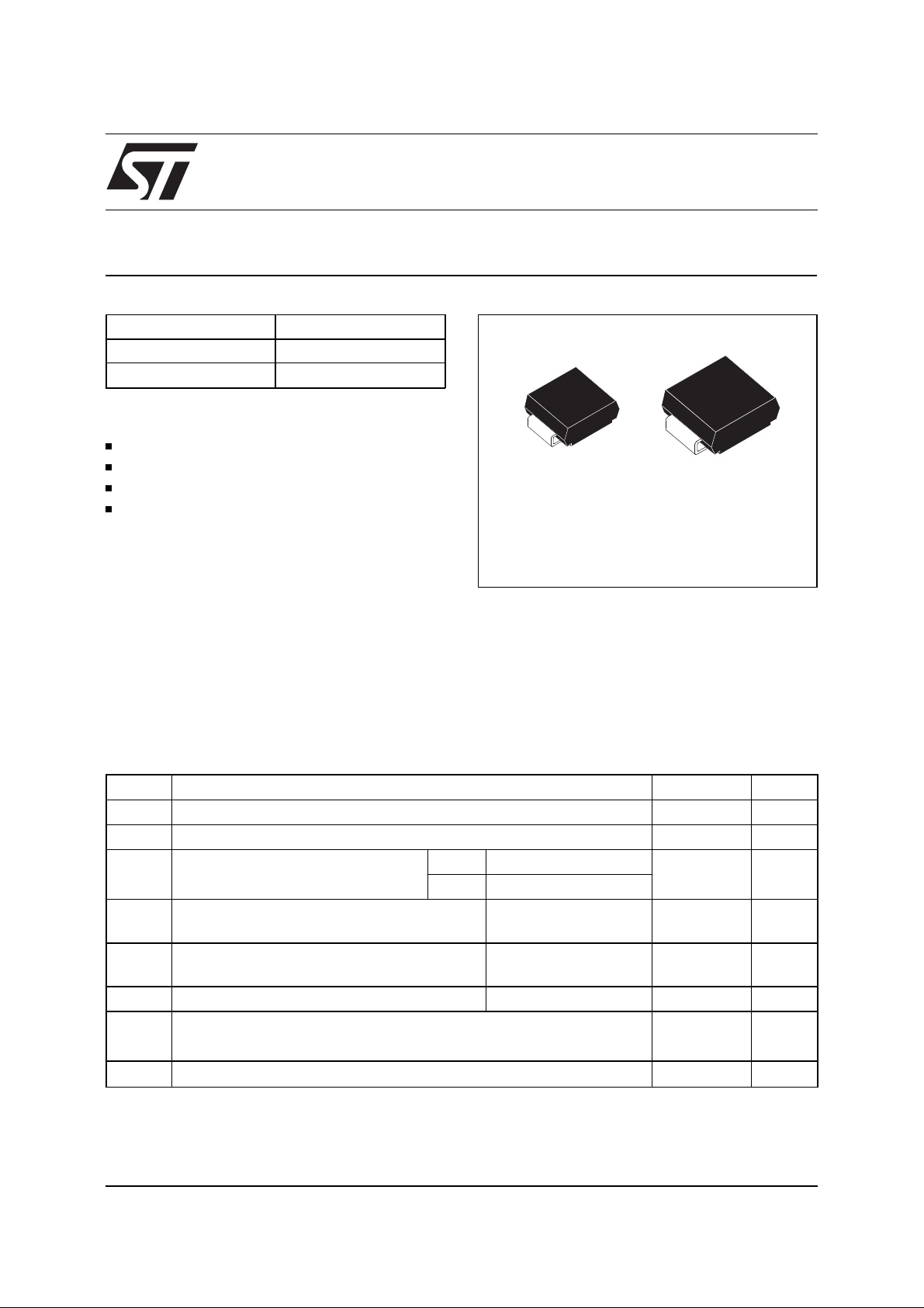
DESCR IPTIO N
Single chip Schottky rectifier suited for Switchmode Power Supplies and high frequency DC to
DC converters.
Packaged in SMA and SMB(*), this device is intended for surface mounting and used in low voltage, high frequency inverters, free wheeling and
polarity protection applications.
(*) in accordance with DO214AAand DO21AC JEDEC
ABSOLUTE RATINGS (limiting values)
SMA
STPS140A
SMB
STPS140U
Symbol Parameter Value Unit
V
RRM
I
F(RMS)
I
F(AV)
I
FSM
Repetitive peak reverse voltage 40 V
RMS forward current 7 A
Average forward current
Surge non repetitive forward current tp = 10 ms
δ
= 0.5 SMA TL = 130°C 1 A
SMB T
= 135°C
L
60 A
Sinusoidal
I
RRM
Repetitive peak reverse current tp = 2 µs
1A
F = 1kHz
I
RSM
T
stg
Non repetitive peak reverse current tp = 100µs square 1 A
Storage temperature range - 65 to + 150
Tj Maximum junction temperature 150
dV/dt Critical rate of rise of reverse voltage 10000 V/µs
July 1998 - Ed: 6B
°
C
1/6
Page 2
STPS140A/U
THERMAL RE SISTA NC ES
Symbol Parameter Value Unit
R
th (j -l)
Junction to lead SMA 30
°
SMB 25
STATIC ELECTRICAL CHARACTE RISTICS
Symbol Tests Conditions Tests Conditions Min. Typ. Max. Unit
* Reverse leakage current Tj = 25°CV
I
R
= 40V 12
R
Tj = 100°C 0.25 2 mA
** Forward voltage drop Tj = 25°CI
V
F
Tj = 125°CI
Tj = 25°CI
Tj = 125°CI
Pulse test : * tp = 5 ms, δ < 2 %
** tp = 380 µs, δ < 2%
= 1 A 0.55 V
F
= 1 A 0.43 0.5
F
= 2 A 0.65
F
= 2 A 0.53 0.6
F
To evaluate the maximum conduction losses use the following equation :
P = 0.4 x I
F(AV)
+ 0.10 x I
F2(RMS)
C/W
µ
A
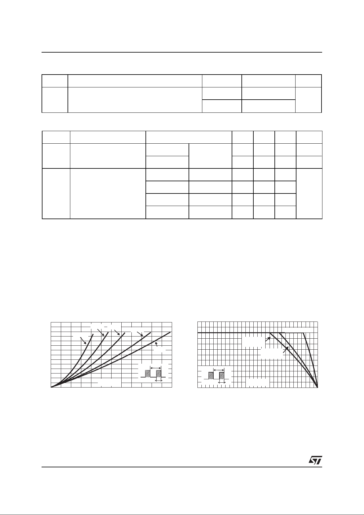
Fig. 1:
Average forward power dissipation versus
average forward current.
PF(av)(W)
0.7
0.6
0.5
0.4
0.3
0.2
0.1
0.0
0.0 0.2 0.4 0.6 0.8 1.0 1.2
δ = 0.05
2/6
= 0.1δ
IF(av) (A)
= 0.2δ
= 0.5δ
= 1δ
T
=tp/T
δ
Fig. 2:
Average forward current versus ambient
temperature (δ=0.5).
IF(av)(A)
1.2
1.0
0.8
0.6
0.4
tp
0.2
0.0
0 25 50 75 100 125 150
δ
T
=tp/T
SMA
Rth(j-a)=100°C/W
S(Cu)=1.5cm²
tp
SMB
Rth(j-a)=80°C/W
S(Cu)=1.5cm²
Tamb(°C)
Rth(j-a)=Rth(j-l)
Page 3

STPS140A/U
Fig. 3-1:
Non repetivesurge peak forward current
versus ove rload duration (maximum va lues) (SMB).
IM(A)
8
7
6
5
4
3
2
I
M
1
0
1E-3 1E-2 1E-1 1E+0
Fig. 4-1:
t
δ
=0.5
t(s)
Relative variation of thermal impedance
Ta=25°C
Ta=50°C
Ta=100°C
junction to ambient versus pulse duration (SMB).
Zth(j-a)/Rth(j-a)
1.0
Printed circuit board: SCu=1.5cm (e=35µm)
0.9
0.8
0.7
0.6
= 0.5δ
0.5
0.4
0.3
= 0.2δ
0.2
= 0.1δ
0.1
0.0
1E-2 1E-1
2
Single pulse
1E+0
tp(s)
1E+1 1E+2
δ
=tp/T
T
tp
1E+3
Fig. 3-2:
Non repetivesurge peak forward current
versus ov erload dura tion (maximum v alues) (SMA).
IM(A)
8
7
6
5
Ta=25°C
4
3
2
I
M
1
0
1E-3 1E-2 1E-1 1E+0
Fig. 4-2:
t
δ
=0.5
t(s)
Relative variation of thermal impedance
Ta=50°C
Ta=100°C
junction to ambient versus puls e dur ation (S MA).
Zth(j-a)/Rth(j-a)
1.0
Printed circuit board: SCu=1.5cm (e=35µm)
0.9
0.8
0.7
0.6
= 0.5δ
0.5
0.4
0.3
= 0.2δ
0.2
= 0.1δ
0.1
0.0
1E-2 1E-1 1E+0 1E+1 1E+2
2
Single pulse
tp(s)
δ
=tp/T
T
tp
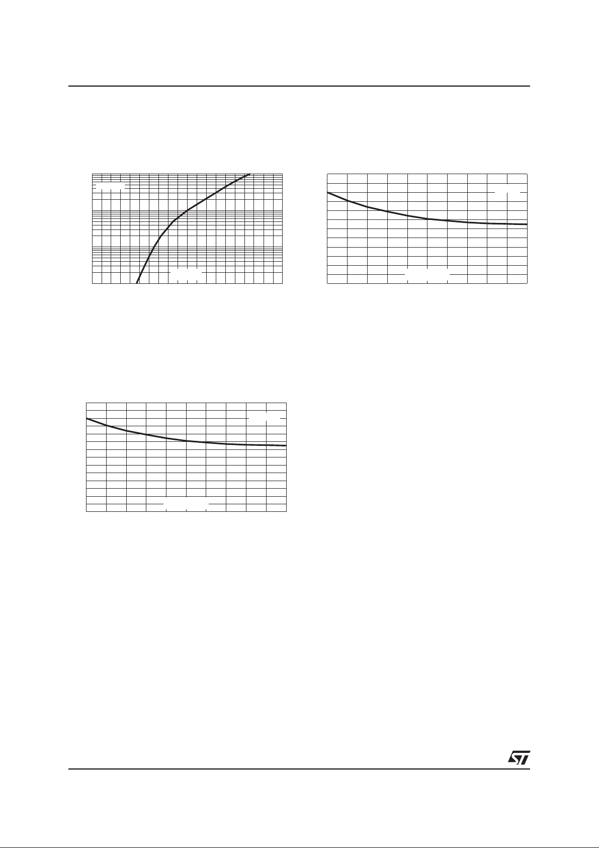
Fig. 5:
Reverse leakage current versus reverse
voltage applied (typical values).
IR(µA)
1E+3
1E+2
1E+1
1E+0
1E-1
1E-2
Tj=125°C
Tj=75°C
Tj=25°C
VR(V)
0 5 10 15 20 25 30 35 40
Fig. 6:
Junction capacitance versus reverse
voltage applied (typical values)
C(pF)
200
100
50
20
VR(V)
10
12 51020 50
F=1MHz
Tj=25°C
3/6
Page 4
STPS140A/U
Fig. 7:
Forward voltage drop versus forward
current (maximum values).
IFM(A)
1E+1
Tj=125°C
1E+0
1E-1
1E-2
0.0 0.1 0.2 0.3 0.4 0.5 0.6 0.7 0.8 0.9 1.0
Fig. 8-2:
Thermal resistance junction to ambient
VFM(V)
versus copper surface under each lead (Epoxy
printed circui t board, copper th ickness: 35µm)(SMA ).
Rth(j-a) (°C/W)
140
120
100
80
60
40
20
0
012345
S(Cu) (cm²)
P=1.5W
Fig. 8-1:
Thermal resistance junction to ambient
versus copper surface under each lead (Epoxy
printed circ uit board, copper thickness : 35µm)(SM B).
Rth(j-a) (°C/W)
120
100
80
60
40
20
0
012345
S(Cu) (cm²)
P=1.5W
4/6
Page 5

PACKAGE MECHANICAL DAT A
SMA
STPS140A/U
DIMENSIONS
C
FOOT PRINT
E1
E
L
(in millimeters)
REF.
Millimeters Inches
Min. Max. Min. Max.
A1 1.90 2.70 0.075 0.106
D
A2 0.05 0.20 0.002 0.008
b 1.25 1.65 0.049 0.065
c 0.15 0.41 0.006 0.016
E 4.80 5.60 0.189 0.220
A1
A2
b
E1 3.95 4.60 0.156 0.181
D 2.25 2.95 0.089 0.116
L 0.75 1.60 0.030 0.063
Marking:
S140
1.45 1.45
2.40
1.65
5/6
Page 6

STPS140A/U
PACKAGE MECHANICAL DAT A
SMB Plastic
DIMENSIONS
C
FOOT PRINT
E1
E
L
(in millimeters)
REF.
Millimeters Inches
Min. Max. Min. Max.
A1 1.90 2.45 0.075 0.096
D
A2 0.05 0.20 0.002 0.008
b 1.95 2.20 0.077 0.087
c 0.15 0.41 0.006 0.016
E 5.10 5.60 0.201 0.220
A1
A2
b
E1 4.05 4.60 0.159 0.181
D 3.30 3.95 0.130 0.156
L 0.75 1.60 0.030 0.063
Marking:
G14
2.3
1.52 2.75
Information furnished is believed to be accurate and reliable. However, STMicroelectronics assumes no responsibility for the consequences of
use of such information nor for any infringement of patents or other rights of third parties which may result from its use. No license is granted by
implication or oth erwise under any patent or patent rights of STMi croelectronics . Specifications mentioned i n this publication are subjec t to
change without notice. This publication supersedes and replaces all information previously supplied.
STMicroelectr oni cs products are n ot authorized for use as critical component s in life support devi ces or systems wi t hout express written approval of STMicroelectronics.
© 1999 STMicroelectronics - Printed in Italy - All rights reserved.
Australia - Brazil - China - Finland - France - Germany - Hong Kong - India - Italy - Japan - Malaysia
Malta - Morocco - Singapore - Spain - Sweden - Switzerland - United Kingdom - U.S.A.
1.52
The ST logo is a registered trademark o f STMicroelectron ics
STMicroelectronics GROUP OF COMPANIES
6/6
 Loading...