

Page 1
MAINPRODUCTCHARACTERISTICS
STPS130A/U
SCHOTTKYRECTIFIER
I
F(AV)
V
RRM
(max) 0.46V
V
F
1A
30 V
FEATURES AND BENEFITS
LOW DROP FORWARD VOLTAGE FOR LESS
POWERDISSIPATIONAND LOWLEAKAGE
OPTIMIZED CONDUCTION / REVERSE
LOSSES TRADE-OFF ALLOWING THE HIGHESTEFFICIENCYINAPPLICATION
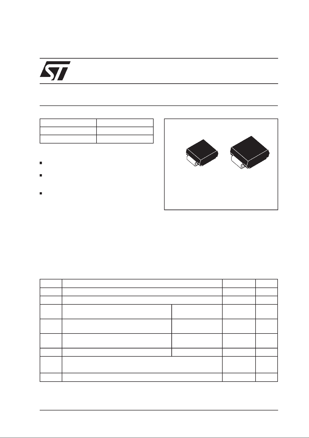
SURFACEMOUNTMINIATUREPACKAGE
DESCRIPTION
Single Schottky rectifier suited to Switched Mode
Power Supplies and high frequency DC/DC converters.
Packaged in SMA or SMB(*), this device is especiallyintended for usein parallel with MOSFETsin
synchronous rectification and low voltage secondaryrectification.
(*)in accordance with DO214AAand DO214AC JEDEC
ABSOLUTERATINGS (limitingvalues)
SMA
STPS130A
SMB
STPS130U
Symbol Parameter Value Unit
V
RRM
I
F(RMS)
I
F(AV)
Repetitivepeak reverse voltage 30 V
RMSforwardcurrent 7 A
Averageforward current TL= 135°C
1A
δ = 0.5
I
FSM
Surgenon repetitive forward current tp = 10ms
45 A
Sinusoidal
I
RRM
Repetitivepeak reverse current tp =2µs
1A
F =1kHz
I
RSM
T
stg
Non repetitivepeak reversecurrent tp = 100µs square 1 A
Storagetemperaturerange - 65 to + 150 °C
Tj Maximumjunction temperature 150
dV/dt Criticalrate of riseof reversevoltage 10000 V/µs
July 1998 - Ed: 5A
1/6
Page 2
STPS130A/U
THERMALRESISTANCES
Symbol Parameter Value Unit
R
th (j-l)
Junctionto lead SMA 30 °C/W
SMB 25
STATIC ELECTRICAL CHARACTERISTICS
Symbol Tests Conditions Tests Conditions Min. Typ. Max. Unit
* Reverseleakagecurrent Tj = 25°CV
I
R
=30V 10 µA
R
Tj = 125°C 1.5 10 mA
** Forwardvoltage drop Tj = 25°CI
V
F
Tj = 125°CI
Tj=25°CI
Tj = 125°CI
Pulse test : * tp= 380 µs, δ <2%
** tp= 5ms,δ <2%
= 1 A 0.55 V
F
= 1 A 0.37 0.46
F
= 2 A 0.63
F
= 2 A 0.45 0.55
F
To evaluatethe maximum conductionlossesuse the followingequation:
P = 0.37 x I
F(AV)
+ 0.090x I
F2(RMS)
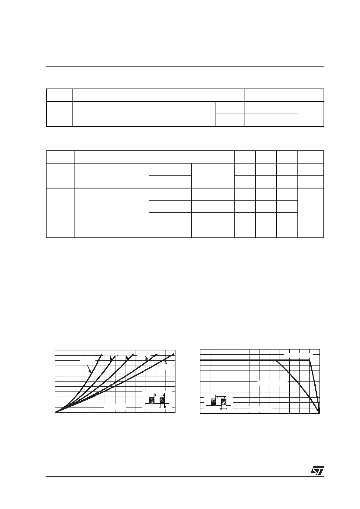
Fig. 1:
Averageforward power dissipationversus
averageforwardcurrent.
PF(av)(W)
0.6
0.5
0.4
0.3
0.2
0.1
0.0
0.0 0.2 0.4 0.6 0.8 1.0 1.2
δ= 0.05
2/6
δ = 0.1 δ= 0.2
IF(av) (A)
δ = 0.5
δ
δ =1
T
=tp/T
Fig. 2:
Average forward current versus ambient
temperature(δ=0.5).
IF(av)(A)
1.2
1.0
0.8
0.6
0.4
tp
0.2
0.0
0 25 50 75 100 125 150
T
=tp/T tp
δ
Rth(j-a)=100°C/W
Tamb(°C)
Rth(j-a)=Rth(j-l)
Page 3

STPS130A/U
Fig. 3-1: Nonrepetitivesurgepeakforwardcurrent
versusoverloadduration(maximumvalues)(SMB).
IM(A)
8
7
6
5
Ta=50°C
Ta=75°C
4
3
IM
2
1
0
1.0E-3 1.0E-2 1.0E-1 1.0E+0
δ=0.5
t
t(s)
Ta=100°C
Fig.4-1: Relative variationof thermal impedance
junction to ambient versus pulseduration(epoxy
printedcircuitboard,S(Cu)=35mm,recommended
padlayout).(SMB)
Zth(j-a)/Rth(j-a)
1.0
Fig. 3-2: Nonrepetitivesurgepeakforwardcurrent
versusoverloadduration(maximumvalues)(SMA).
IM(A)
8
7
6
5
Ta=50°C
Ta=75°C
4
3
2
IM
1
0
1.0E-3 1.0E-2 1.0E-1 1.0E+0
δ=0.5
t
Ta=100°C
t(s)
Fig.4-2: Relative variationofthermalimpedance
junction to ambient versus pulse duration(epoxy
printedcircuitboard,S(Cu)=35mm,recommended
pad layout).(SMA)
Zth(j-a)/Rth(j-a)
1.0
0.8
0.6
δ = 0.5
0.4
δ = 0.2
0.2
δ = 0.1
0.0
1.0E-2 1.0E-1 1.0E+0 1.0E+1 1.0E+2 1.0E+3
Single pulse
tp(s)
δ
=tp/T
T
tp
Fig. 5: Reverse leakage current versus reverse
voltageapplied (typicalvalues).
IR(µA)
5E+3
1E+3
1E+2
1E+1
1E+0
1E-1
0 5 10 15 20 25 30
Tj=125°C
Tj=70°C
Tj=25°C
VR(V)
0.8
0.6
δ = 0.5
0.4
δ
=tp/T
T
tp
δ = 0.2
0.2
δ = 0.1
0.0
1E-2 1E-1 1E+0 1E+1 1E+2 1E+3
Single pulse
tp(s)
Fig. 6: Junction capacitance ve rsus reverse
voltage applied(typicalvalues).
C(pF)
500
F=1MHz
200
100
50
20
VR(V)
10
12 5102030
Tj=25°C
3/6
Page 4

STPS130A/U
Fig. 7:
Forward voltage drop versus forward cur-
rent(maximum values).
IFM(A)
10.00
1.00
0.10
0.01
0.0 0.2 0.4 0.6 0.8 1.0 1.2
Fig. 8-2:
Tj=75°C
Tj=125°C
Tj=25°C
VFM(V)
Thermal resistance junction to ambient
versus coppe r surface under each lead (Epoxy
printed circuit board, copper thickness:
35µm).(SMA)
Rth(j-a) ( °C/W)
140
120
100
80
60
40
20
0
012345
S(Cu) (cm )
P=1.5W
Fig. 8-1:
Thermal resistance junction to ambient
versus copper surface under each lead (Epoxy
printed circuit board, copper thickness:
35µm).(SMB)
Rth(j-a) ( °C/W)
120
100
80
60
40
20
0
012345
S(Cu) (cm )
P=1.5W
4/6
Page 5

PACKAGEMECHANICAL DATA
SMA
STPS130A/U
DIMENSIONS
C
FOOTPRINT
E1
E
L
(in millimeters)
REF.
Millimeters Inches
Min. Max. Min. Max.
A1 1.90 2.70 0.075 0.106
D
A2 0.05 0.20 0.002 0.008
b 1.25 1.65 0.049 0.065
c 0.15 0.41 0.006 0.016
E 4.80 5.60 0.189 0.220
A1
A2
b
E1 3.95 4.60 0.156 0.181
D 2.25 2.95 0.089 0.116
L 0.75 1.60 0.030 0.063
Marking:S130
Cathodeband indicatescathode
1.45 1.45
2.40
1.65
5/6
Page 6

STPS130A/U
PACKAGEMECHANICAL DATA
SMB
DIMENSIONS
REF.
E1
A1 1.90 2.45 0.075 0.096
D
A2 0.05 0.20 0.002 0.008
b 1.95 2.20 0.077 0.087
c 0.15 0.41 0.006 0.016
E
E 5.10 5.60 0.201 0.220
A1
C
L
A2
b
E1 4.05 4.60 0.159 0.181
D 3.30 3.95 0.130 0.156
L 0.75 1.60 0.030 0.063
FOOTPRINT (in millimeters) Marking:
Cathodeband indicatescathode
Millimeters Inches
Min. Max. Min. Max.
G12
2.3
1.52 2.75
Informationfurnished isbelieved to be accurate and reliable.However, STMicroelectronicsassumes noresponsIbility for theconsequences of
use of such informationnor forany infringementof patents or other rights of thirdparties which may result from itsuse. Nolicense is granted by
implication or otherwise under any patent or patent rights of STMicroelectronics. Specifications mentioned in thispublication are subject to
change without notice. This publication supersedes and replaces all information previouslysupplied.
STMicroelectronics products are not authorized for use as critical components in lifesupport devices or systems withoutexpress written approval of STMicroelectronics.
1998 STMicroelectronics - Printedin Italy - Allrights reserved.
Australia - Brazil - Canada - China - France - Germany - Italy - Japan -Korea - Malaysia - Malta- Mexico - Morocco -
The Netherlands Singapore - Spain - Sweden - Switzerland - Taiwan - Thailand - United Kingdom - U.S.A.
6/6
1.52
The ST logo is aregistered trademark of STMicroelectronics
STMicroelectronicsGROUP OF COMPANIES
 Loading...