

Page 1
®
Table 1: Main Product Characteristics
I
V
T
j
V
F
F(AV)
RRM
(max)
(max)
1 A
20 V
150°C
0.41 V
STPS120M
POWER SCHOTTKY RECTIFIER
A
C
FEATURES AND BENEFITS
■ Very small conduction losses
■ Negligible switching losses
■ Extremely fast switching
■ Low forward voltage drop for higher efficiency
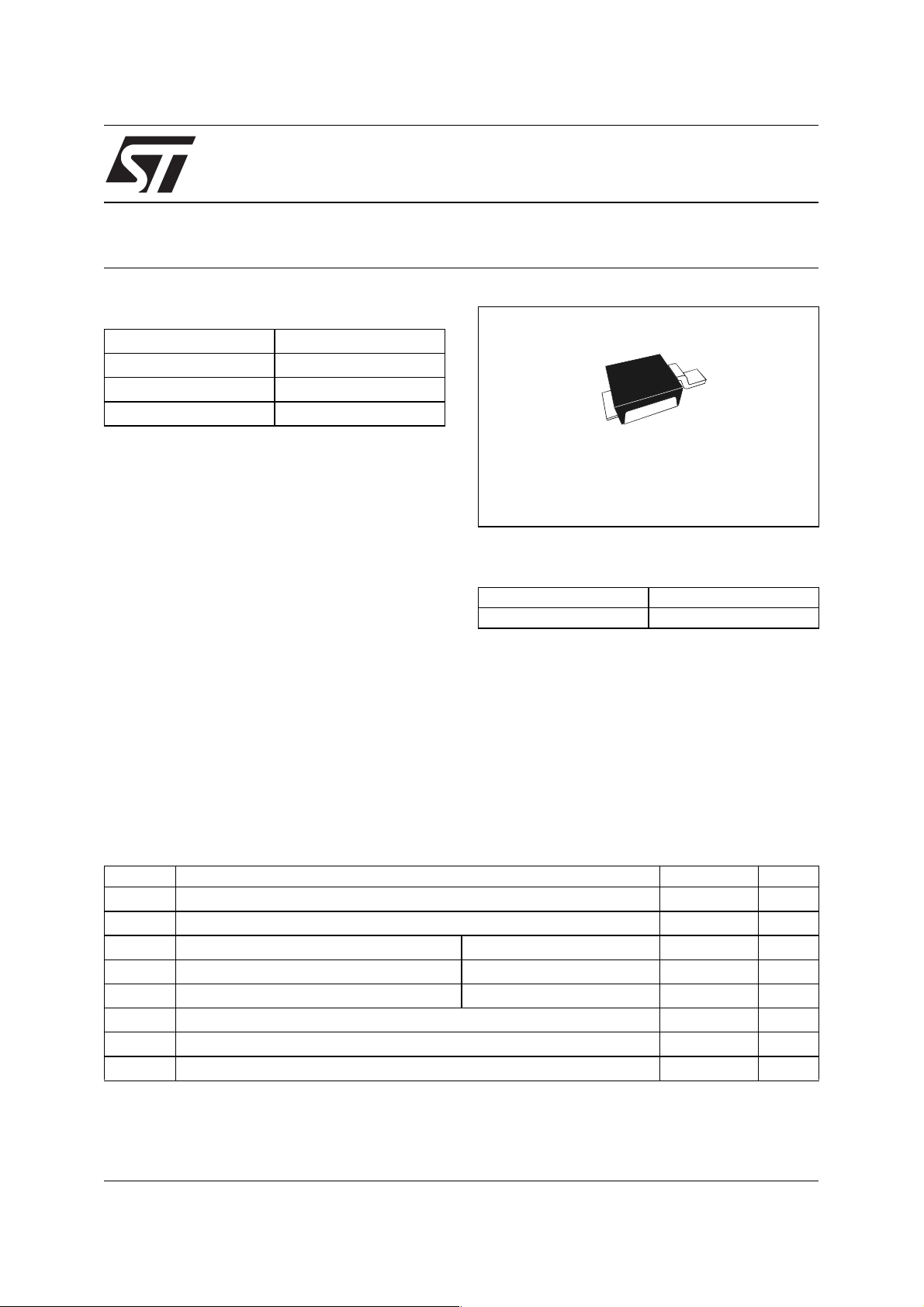
STmite
(DO216-AA)
and extented battery life
■ Low thermal resistance
■ Avalanche capability specified
DESCRIPTION
Table 2: Order Code
Part Number Marking
STPS120M 120
Single Schottky rectifier suited for switch mode
power supplies and high frequency DC to DC
converters.
Packaged in STmite, this device is intended for
use in low voltage, high frequency inverters, free
wheeling and polarity protection applications. Due
to the small size of the package this device fits
battery powered equipment (cellular, notebook,
PDA’s, printers) as well chargers and PCMCIA
cards.
Table 3: Absolute Ratings (limiting values)
Symbol Parameter Value Unit
V
RRM
I
F(RMS)
I
F(AV)
I
FSM
P
ARM
T
T
dV/dt
dPtot
* : thermal runaway condition for a diode on its own heatsink
------------- --
dTj
Repetitive peak reverse voltage 20 V
RMS forward voltage 2 A
T
Average forward current
= 140°C δ = 0.5
c
Surge non repetitive forward current tp = 8.3 ms sinusoidal 50 A
Repetitive peak avalanche power tp = 1µs Tj = 25°C 1400 W
Storage temperature range -65 to + 150 °C
stg
Maximum operating junction temperature * 150 °C
j
Critical rate of rise of reverse voltage (rated V
1
--------------- ----------->
Rth j a
–()
, Tj = 25°C)
R
10000 V/µs
1A
September 2004
REV. 3
1/6
Page 2
STPS120M
Table 4: Thermal Resistance
Symbol Parameter Value Unit
*
R
th(j-c)
R
th(j-l)
* Mounted with minimum recommended pad size, PC board FR4.
Table 5: Static Electrical Characteristics
Symbol Parameter Tests conditions Min. Typ Max. Unit
I
R
V
Junction to case 20 °C/W
* Junction to ambient
*
Reverse leakage current
*
Forward voltage drop
F
T
= 25°C
j
T
= 100°C
j
T
= 25°C VR = 10V
j
T
= 100°C
j
= 25°C VR = 5V
T
j
= 100°C
T
j
= 25°C
T
j
T
= 100°C
j
= 25°C
T
j
T
= 100°C
j
V
R
I
F
I
F
= V
= 1A
= 3A
RRM
250
1.3 3.9
275 850
0.6 2.0
145 450
0.4 1.0
105 300
0.44 0.49
0.36 0.41
0.48 0.54
0.42 0.48
°C/W
µA
V
Pulse test: * tp = 380 µs, δ < 2%
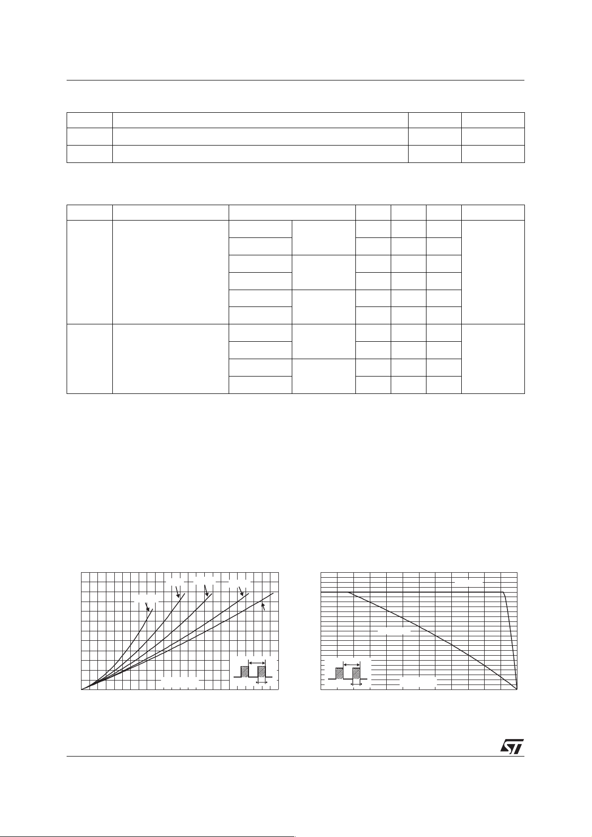
To evaluate the conduction losses use the following equation: P = 0.34 x I
Figure 1: Conduction losses versus average
current
P (W)
F(AV)
0.6
0.5
0.4
0.3
0.2
0.1
0.0
0.0 0.1 0.2 0.3 0.4 0.5 0.6 0.7 0.8 0.9 1.0 1.1 1.2
δ = 0.05
δ = 0.1
I (A)
F(AV)
δ = 0.2
δ = 0.5
=tp/T
δ
δ = 1
T
tp
+ 0.07 I
F(AV)
F2(RMS)
Figure 2: Average forward current versus
ambient temperature (δ = 0.5)
I (A)
F(AV)
1.2
1.1
1.0
0.9
0.8
0.7
0.6
0.5
0.4
0.3
0.2
0.1
=tp/T
δ
0.0
0 25 50 75 100 125 150
R =270°C/W
th(j-a)
T
T (°C)
tp
amb
R=R
th(j-a) th(j-c)
2/6
Page 3

STPS120M
Figure 3: Normalized avalanche power
derating versus pulse duration
P(t)
ARM p
P (1µs)
ARM
1
0.1
0.01
t (µs)
0.001
0.10.01 1
p
10 100 1000
Figure 5: Non repetitive surge peak forward
current versus overload duration (maximum
values)
I (A)
M
22
20
18
16
14
12
10
8
6
4
I
M
2
0
1.E-03 1.E-02 1.E-01 1.E+00
t
δ
=0.5
t(s)
T =25°C
C
T =75°C
C
T =125°C
C
Figure 4: Normalized avalanche power
derating versus junction temperature
P(t)
ARM p
P (25°C)
ARM
1.2
1
0.8
0.6
0.4
0.2
0
25 50 75 100 125 150
T (°C)
j
Figure 6: Relative variation of thermal
impedance junction to ambient versus pulse
duration
Z/R
th(j-c) th(j-c)
1.0
0.9
0.8
0.7
0.6
δ = 0.5
0.5
0.4
0.3
δ = 0.2
0.2
δ = 0.1
0.1
Single pulse
0.0
1.E-04 1.E-03 1.E-02 1.E-01
t (s)
p
δ
=tp/T
T
tp
Figure 7: Reverse leakage current versus
reverse voltage applied (typical values)
I (mA)
R
1.E+01
T =150°C
j
1.E+00
1.E-01
1.E-02
1.E-03
1.E-04
02468101214161820
T =125°C
j
T =100°C
j
T =75°C
j
T =50°C
j
T =25°C
j
V (V)
R
Figure 8: Junction capacitance versus reverse
voltage applied (typical values)
C(pF)
1000
100
V (V)
10
110100
R
F=1MHz
V =30mV
OSC RMS
T =25°C
j
3/6
Page 4

STPS120M
Figure 9: Forward voltage drop versus forward
current (low level)
I (A)
FM
2.0
1.8
1.6
1.4
1.2
1.0
0.8
0.6
0.4
0.2
0.0
0.0 0.1 0.2 0.3 0.4 0.5 0.6
(maximum values)
T =100°C
j
(typical values)
T =100°C
j
T =25°C
j
(maximum values)
V (V)
FM
Figure 11: Thermal resistance junction to
ambient versus copper surface under tab
(epoxy printed board FR4, Cu = 35µm, typical
values)
R (°C/W)
th(j-a)
300
250
Figure 10: Forward voltage drop versus
forward current (high level)
I (A)
FM
100.0
T =100°C
j
10.0
1.0
0.1
0.0 0.2 0.4 0.6 0.8 1.0 1.2 1.4
(maximum values)
T =100°C
j
(typical values)
T =25°C
j
(maximum values)
V (V)
FM
200
150
100
50
0
0.0 0.2 0.4 0.6 0.8 1.0 1.2 1.4 1.6 1.8 2.0
S(cm²)
4/6
Page 5

Figure 12: STmite Package Mechanical Data
L3
D
b2
H
C
R1
b
L2
L
R
A
A1
0° to 6°
STPS120M
DIMENSIONS
REF.
A 0.85 1.00 1.15 0.033 0.039 0.045
A1 -0.05 0.05 -0.002 0.002
b 0.40 0.65 0.016 0.025
b2 0.70 1.00 0.027 0.039
c 0.10 0.25 0.004 0.010
D 1.75 1.90 2.05 0.069 0.007 0.081
E
E 1.75 1.90 2.05 0.069 0.007 0.081
H 3.60 3.75 3.90 0.142 0.148 0.154
L 0.50 0.63 0.80 0.020 0.025 0.031
L2 1.20 1.35 1.50 0.047 0.053 0.059
L3 0.50
R 0.07 0.003
R1 0.07 0.003
Millimeters Inches
Min. Typ. Max. Min. Typ. Max.
0.019
ref
ref
Figure 13: Foot Print Dimensions (in millimeters)
1.82
1.38
2.03
1.10
0.50
0.71
0.75
Table 6: Ordering Information
Ordering type Marking Package Weight Base qty Delivery mode
STPS120M 120 STmite 15.5 mg 12000 Tape & reel
Table 7: Revision History
Date Revision Description of Changes
Jul-2003 2A Last update.
13-Sep-2004 3
STmite package dimensions reference A1 change: from
blank (min) to -0.05mm and from 0.10 (max) to 0.05mm.
5/6
Page 6

STPS120M
Information furnished is believed to be accurate and reliable. However, STMicroelectronics assumes no responsibility for the consequences
of use of such information nor for any infringement of patents or other rights of third parties which may result from its use. No license is granted
by implication or otherwise under any patent or patent rights of STMicroelectronics. Specifications mentioned in this publication are subject
to change without notice. This publication supersedes and replaces all information previously supplied. STMicroelectronics products are not
authorized for use as critical components in life support devices or systems without express written approval of STMicroelectronics.
The ST logo is a registered trademark of STMicroelectronics.
All other names are the property of their respective owners
© 2004 STMicroelectronics - All rights reserved
Australia - Belgium - Brazil - Canada - China - Czech Republic - Finland - France - Germany - Hong Kong - India - Israel - Italy - Japan -
Malaysia - Malta - Morocco - Singapore - Spain - Sweden - Switzerland - United Kingdom - United States of America
STMicroelectronics group of companies
www.st.com
6/6
 Loading...