

Page 1

®
STPS10H100CT/CG/CR/CFP
HIGH VOLTAGE POWER SCHOTTKY RECTIFIER
MAIN PRODUCT CHARACTERISTICS
I
F(AV)
V
RRM
2x5A
100 V
Tj 175°C
V
(max) 0.61 V
F
FEATURES AND BENEFITS
HIGH JUNCTION TEMPERATURE CAPABILITY
■
FOR CONVERTERS LOCATED IN CONFINED
ENVIRONMENT
LOW LEAKAGE CURRENT AT HIGH
■
TEMPERATURE
LOW STATIC AND DYNAMIC LOSSES AS A
■
RESULT OF THE SCHOTTKY BARRIER
■ AVALANCHE CAPABILITY SPECIFIED
DESCRIPTION
Schottky barrier rectifier designed for high
frequency miniature Switched Mode Power
Supplies such as adaptators and on board
DC/DC converters. Packaged in TO-220AB,
TO-220FPAB, D
2
PAK and I2PAK.
A1
A2
K
A2
A1
D2PAK
STPS10H100CG
A1
TO-220AB
STPS10H100CT
K
K
A2
K
A1
I2PAK
STPS10H100CR
A1
A2
K
A2
K
TO-220FPAB
STPS10H100CFP
ABSOLUTE RATINGS (limiting values, per diode)
Symbol Parameter Value Unit
V
RRM
I
F(RMS)
I
F(AV)
Repetitive peak reverse voltage 100 V
RMS forward current 10 A
Average forward
current δ = 0.5
TO-220AB
D2PAK/I2PAK
Tc = 165°C per diode
per device
5
10
TO-220FPAB Tc = 160°C
I
I
P
T
FSM
RRM
ARM
Surge non repetitive forward current tp= 10 ms sinusoidal 180 A
Repetitive peak reverse current tp=2µssquare F = 1kHz 1 A
Repetitive peak avalanche power tp = 1µs Tj = 25°C 7200 W
Storage temperature range -65 to+ 175 °C
stg
Tj Maximum operating junction temperature * 175 °C
dV/dt Critical rate of rise of reverse voltage 10000 V/µs
dPtot
*:
<
dTj Rth j a
July 2003 - Ed: 3F
thermal runaway condition for a diode on its own heatsink
−1()
A
1/7
Page 2
STPS10H100CT/CG/CR/CFP
THERMAL RESISTANCES
Symbol Parameter Value Unit
R
th (j-c)
R
th (c)
R
th (j-c)
R
th (c)
When the diodes 1 and 2 are used simultaneously :
∆ Tj(diode 1) = P(diode1) x R
STATIC ELECTRICAL CHARACTERISTICS (per diode)
Symbol Parameter Tests conditions Min. Typ. Max. Unit
I
R
V
F
Junction to case D2PAK / I2PAK
TO-220AB
Per diode 2.2 °C/W
Total 1.3
Coupling 0.3
Junction to case TO-220FPAB Per diode 4.5 °C/W
Total 3.5
Coupling 2.5
(Per diode) + P(diode 2) x R
th(j-c)
* Reverse leakage current Tj= 25°C VR=V
th(c)
RRM
3.5 µA
Tj = 125°C 1.3 4.5 mA
** Forward voltage drop Tj = 25°CI
= 5 A 0.73 V
F
Tj = 125°C 0.57 0.61
Tj=25°CI
= 10 A 0.85
F
Tj = 125°C 0.66 0.71
Pulse test : * tp=5ms,δ<2%
** tp = 380 µs, δ <2%
To evaluate the maximum conduction losses use the following equation :
P=0.51xI
Fig. 1: Average forward power dissipation versus
average forward current (per diode).
PF(av)(W)
4.0
3.5
3.0
2.5
2.0
1.5
1.0
0.5
0.0
0.0 0.5 1.0 1.5 2.0 2.5 3.0 3.5 4.0 4.5 5.0 5.5 6.0
F(AV)
+0.02xI
δ = 0.1
δ = 0.05
F2(RMS)
δ = 0.2
IF(av) (A)
δ = 0.5
δ
=tp/T
δ = 1
T
Fig. 2: Average forward current versus ambient
temperature (δ=0.5, per diode).
IF(av)(A)
6
5
4
3
2
tp
1
0
0 25 50 75 100 125 150 175
Rth(j-a)=Rth(j-c)
D²PAK/I²PAK/TO-220AB
TO-220FPAB
Rth(j-a)=15°C/W
Tamb(°C)
2/7
Page 3

STPS10H100CT/CG/CR/CFP
Fig. 3: Normalized avalanche power derating ver-
sus pulse duration.
P(t)
ARM p
P (1µs)
ARM
1
0.1
0.01
t (µs)
0.001
0.10.01 1
p
10 100 1000
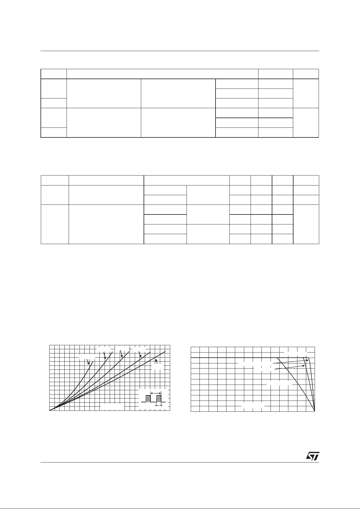
Fig. 5-1: Non repetitive surge peak forward
current versus overload duration (maximum
values, per diode)
IM(A)
120
100
80
60
40
IM
20
0
1E-3 1E-2 1E-1 1E+0
δ=0.5
t
t(s)
Tc=50°C
Tc=75°C
Tc=125°C
Fig. 4: Normalized avalanche power derating
versus junction temperature.
P(t)
ARM p
P (25°C)
ARM
1.2
1
0.8
0.6
0.4
0.2
0
0 25 50 75 100 125 150
T (°C)
j
Fig.5-2: Non repetitivesurge peak forward current
versus overload duration (maximum values, per
diode)(TO-220FPAB)
IM(A)
80
70
60
50
40
30
20
IM
10
0
1E-3 1E-2 1E-1 1E+0
δ=0.5
t
t(s)
Tc=50°C
Tc=75°C
Tc=125°C
Fig. 6-1: Relative variation of thermal impedance
junction to case versus pulse duration (per diode).
Zth(j-c)/Rth(j-c)
1.0
0.8
δ = 0.5
0.6
δ = 0.2
0.4
δ = 0.1
0.2
Single pulse
0.0
1E-3 1E-2 1E-1 1E+0
tp(s)
δ
=tp/T
T
tp
Fig. 6-2: Relative variation of thermal impedance
junction to case versus pulse duration (per
diode).(TO-220FPAB)
Zth(j-c)/Rth(j-c)
1.0
0.8
δ = 0.5
0.6
0.4
δ
=tp/T
T
tp
3/7
δ = 0.2
0.2
δ = 0.1
0.0
Single pulse
1E-3 1E-2 1E-1 1E+0 1E+1
tp(s)
Page 4

STPS10H100CT/CG/CR/CFP
Fig. 7: Reverse leakage current versus reverse
voltage applied (typical values, per diode).
IR(µA)
1E+4
1E+3
1E+2
Tj=150°C
Tj=125°C
Tj=100°C
1E+1
1E+0
1E-1
Tj=25°C
1E-2
0 102030405060708090100
VR(V)
Fig. 9: Forward voltage drop versus forward
current (maximum values, per diode).
IFM(A)
100.0
10.0
Tj=150°C
Typical values
1.0
0.1
0.0 0.2 0.4 0.6 0.8 1.0 1.2 1.4
Tj=125°C
Typical values
Tj=125°C
Tj=25°C
VFM(V)
Fig. 8: Junction capacitance versus reverse
voltage applied (typical values, per diode).
C(pF)
1000
F=1MHz
Tj=25°C
100
10
1 2 5 10 20 50 100
VR(V)
Fig. 10: Thermal resistance junction to ambient
versus copper surface under tab (Epoxy printed
circuitboard FR4, copper thickness: 35µm)
Rth(j-a) (°C/W)
80
70
60
50
40
30
20
10
0
0 2 4 6 8 101214161820
S(Cu) (cm²)
4/7
Page 5

STPS10H100CT/CG/CR/CFP
PACKAGE MECHANICAL DATA
2
PAK
D
E
L2
L
L3
A1
B2
B
G
* FLAT ZONE NO LESS THAN 2mm
C2
DIMENSIONS
A
REF.
Millimeters Inches
Min. Max. Min. Max.
A 4.40 4.60 0.173 0.181
A1 2.49 2.69 0.098 0.106
D
A2 0.03 0.23 0.001 0.009
B 0.70 0.93 0.027 0.037
B2 1.14 1.70 0.045 0.067
C 0.45 0.60 0.017 0.024
C2 1.23 1.36 0.048 0.054
C
R
D 8.95 9.35 0.352 0.368
E 10.00 10.40 0.393 0.409
G 4.88 5.28 0.192 0.208
A2
L 15.00 15.85 0.590 0.624
L2 1.27 1.40 0.050 0.055
L3 1.40 1.75 0.055 0.069
M
*
V2
M 2.40 3.20 0.094 0.126
R 0.40 typ. 0.016 typ.
V2 0° 8° 0° 8°
FOOT PRINT in millimeters
16.90
10.30
8.90
5.08
1.30
3.70
5/7
Page 6

PACKAGE MECHANICAL DATA
2
PAK
I
E
L2
L1
L
e
b2
b1
b
c2
D
A1
STPS10H100CT/CG/CR/CFP
DIMENSIONS
REF.
A
A 4.40 4.60 0.173 0.181
A1 2.49 2.69 0.098 0.106
b 0.70 0.93 0.028 0.037
b1 1.14 1.17 0.044 0.046
b2 1.14 1.17 0.044 0.046
c 0.45 0.60 0.018 0.024
c2 1.23 1.36 0.048 0.054
D 8.95 9.35 0.352 0.368
e 2.40 2.70 0.094 0.106
E 10.0 10.4 0.394 0.409
L 13.1 13.6 0.516 0.535
c
L1 3.48 3.78 0.137 0.149
L2 1.27 1.40 0.050 0.055
Millimeters Inches
Min. Max. Min. Max.
PACKAGE MECHANICAL DATA
TO-220FPAB
H
Dia
L6
L2
L3
L5
D
L4
G1
G
F1
F2
F
REF. DIMENSIONS
Millimeters Inches
A
B
A 4.4 4.6 0.173 0.181
Min. Max. Min. Max.
B 2.5 2.7 0.098 0.106
D 2.5 2.75 0.098 0.108
E 0.45 0.70 0.018 0.027
F 0.75 1 0.030 0.039
F1 1.15 1.70 0.045 0.067
L7
F2 1.15 1.70 0.045 0.067
G 4.95 5.20 0.195 0.205
G1 2.4 2.7 0.094 0.106
H 10 10.4 0.393 0.409
L2 16 Typ. 0.63Typ.
L3 28.6 30.6 1.126 1.205
L4 9.8 10.6 0.386 0.417
E
L5 2.9 3.6 0.114 0.142
L6 15.9 16.4 0.626 0.646
L7 9.00 9.30 0.354 0.366
Dia. 3.00 3.20 0.118 0.126
6/7
Page 7

STPS10H100CT/CG/CR/CFP
PACKAGE MECHANICAL DATA
TO-220AB
H2
Dia
L5
L6
L2
F2
F1
F
G1
G
L9
L4
REF. DIMENSIONS
Millimeters Inches
Min. Max. Min. Max.
A
C
A 4.40 4.60 0.173 0.181
C 1.23 1.32 0.048 0.051
D 2.40 2.72 0.094 0.107
L7
E 0.49 0.70 0.019 0.027
F 0.61 0.88 0.024 0.034
F1 1.14 1.70 0.044 0.066
F2 1.14 1.70 0.044 0.066
G 4.95 5.15 0.194 0.202
D
G1 2.40 2.70 0.094 0.106
H2 10 10.40 0.393 0.409
L2 16.4 typ. 0.645 typ.
L4 13 14 0.511 0.551
L5 2.65 2.95 0.104 0.116
M
E
L6 15.25 15.75 0.600 0.620
L7 6.20 6.60 0.244 0.259
L9 3.50 3.93 0.137 0.154
M 2.6 typ. 0.102typ.
Diam. 3.75 3.85 0.147 0.151
■ Cooling method: C.
■
Recommended torque value: 0.55 m.N
■
Maximum torque value 0.70 m.N
Ordering type Marking Package Weight Base qty Delivery mode
STPS10H100CT STPS10H100CT TO-220AB 2.20g 50 Tube
STPS10H100CFP STPS10H100CFP TO-220FPAB 2.0 g 50 Tube
STPS10H100CG STPS10H100CG D
STPS10H100CG-TR STPS10H100CG D
STPS10H100CR STPS10H100CR I
■
Epoxy meets UL94,V0
Informationfurnishedis believed to be accurate and reliable. However, STMicroelectronics assumes no responsibility for the consequences of
useof such information nor for any infringement of patents or other rights ofthird parties which may result from its use. No license is granted by
implication or otherwise under any patent or patent rights of STMicroelectronics. Specifications mentioned in this publication are subject to
change without notice. This publication supersedes and replaces all information previously supplied.
STMicroelectronics products are not authorized for use as critical components in life support devices or systems without express written
approval of STMicroelectronics.
The ST logo is a registered trademark of STMicroelectronics
© 2003 STMicroelectronics - Printed in Italy - All rights reserved.
STMicroelectronics GROUP OF COMPANIES
Australia - Brazil - Canada - China - Finland - France - Germany
Hong Kong - India - Israel - Italy - Japan - Malaysia - Malta - Morocco - Singapore
Spain - Sweden - Switzerland - United Kingdom - United States.
http://www.st.com
2
PAK 1.48g 50 Tube
2
PAK 1.48g 1000 Tape and reel
2
PAK 1.49g 50 Tube
7/7
Page 8

WWW.ALLDATASHEET.COM
Copyright © Each Manufacturing Company.
All Datasheets cannot be modified without permission.
This datasheet has been download from :
www.AllDataSheet.com
100% Free DataSheet Search Site.
Free Download.
No Register.
Fast Search System.
www.AllDataSheet.com
 Loading...