

Page 1

®
MAIN PRODUCT CHARACTERISTICS
STPS1045B/H
POWER SCHOTTKY RECTIFIER
I
F(AV)
V
RRM
V
(max) 0.57 V
F
10 A
45 V
FEATURES AND BENEFITS
NEGLIGIBLE SWITCHING LOSSES
n
LOW FORWARD DROP VOLTAGE
n
LOW CAPACITANCE
n
HIGH REVERSE AVALANCHE SURGE
n
CAPABILITY
DESCRIPTION
High voltage Schottky rectifier suited for Switch
Mode Power Supplies and other Power
Converters.
Packaged in DPAK and IPAK, these devices are
intended for use in high frequency circuitries
where low switching losses are required.
ABSOLUTE MAXIMUM RATINGS
K
A
DPAK
STPS1045B
K
A
K
A
K
A
IPAK
STPS1045H
Symbol Parameter Value Unit
V
I
F(RMS)
I
RRM
/ pin RMS forward current / pin 7 A
F(AV)
Repetitive peak reverse voltage 45 V
Average forward current Tc = 150°C
10 A
d = 0.5
I
FSM
Surge non repetitive forward current tp = 10 ms
75 A
Sinusoidal
I
RRM
Repetitive peak reverse current tp = 2 µs
1A
F = 1KHz
T
stg
Storage temperature range - 65 to + 175 °C
Tj Maximum junction temperature 175 °C
dV/dt Critical rate of rise of reverse voltage 10000 V/µs
May 2000 - Ed: 2B
1/5
Page 2
STPS1045B/H
THERMAL RESISTANCES
Symbol Parameter Value Unit
R
th (j-c)
STATIC ELECTRICAL CHARACTERISTICS
Symbol Parameter Tests Conditions Min. Typ. Max. Unit
I
R
V
F
Pulse test : * tp = 380 µs, δ <2%
To evaluate the maximum conduction losses use the following equation :
P=0.42xI
Fig. 1: Averageforward power dissipation versus
average forward current.
Junction to case 3 °C/W
* Reverse leakage current Tj = 25°C VR=45V 100 µA
Tj = 125°C 7 15 mA
** Forward voltage drop Tj = 25°C IF= 10 A 0.63 V
**tp = 5 ms, δ <2%
+ 0.015 I
F(AV)
F2(RMS)
Tj = 125°C I
Tj = 25°C I
Tj = 125°C I
= 10 A 0.5 0.57
F
= 20 A 0.84
F
= 20 A 0.65 0.72
F
Fig. 2: Average forward current versus ambient
temperature (δ=0.5).
PF(av)(W)
8
7
δ = 0.05
δ = 0.1
δ = 0.2
δ = 0.5
6
5
δ = 1
4
3
δ
=tp/T
T
tp
2
1
0
0123456789101112
IF(av) (A)
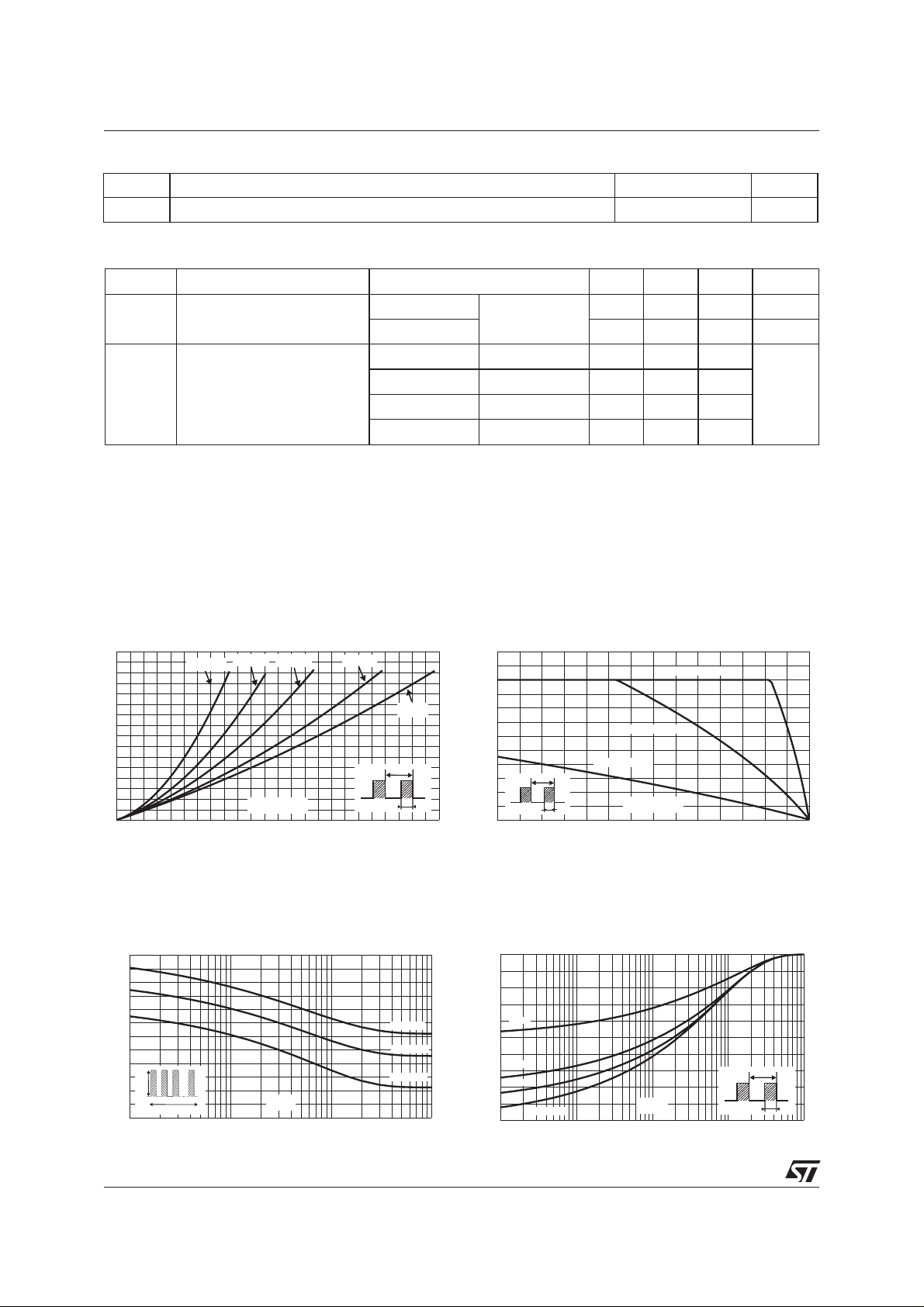
Fig. 3: Non repetitive surge peak forward current
versus overload duration (maximum values).
IM(A)
120
100
80
60
40
IM
20
0
1E-3 1E-2 1E-1 1E+0
δ=0.5
t
t(s)
Tc=50°C
Tc=100°C
Tc=150°C
IF(av)(A)
12
10
Rth(j-a)=Rth(j-c)
8
6
4
T
Rth(j-a)=15°C/W
Rth(j-a)=70°C/W
2
tp
=tp/T
δ
0
0 25 50 75 100 125 150 175
Tamb(°C)
Fig. 4: Relative variation of thermal impedance
junction to case versus pulse duration.
Zth(j-c)/Rth(j-c)
1.0
0.8
δ = 0.5
0.6
0.4
δ = 0.2
δ = 0.1
0.2
0.0
Single pulse
1E-4 1E-3 1E-2 1E-1 1E+0
tp(s)
δ
=tp/T
T
tp
2/5
Page 3

STPS1045B/H
Fig. 5: Reverse leakage current versus reverse
voltage applied (typical values).
IR(µA)
1E+5
1E+4
1E+3
1E+2
1E+1
1E+0
1E-1
0 5 10 15 20 25 30 35 40 45
Tj=150°C
Tj=125°C
Tj=100°C
Tj=75°C
Tj=50°C
Tj=25°C
VR(V)
Fig. 7: Forward voltage drop versus forward
current (maximum values).
IFM(A)
100.0
10.0
Tj=125°C
Tj=125°C
(Typical values)
Tj=25°C
Fig. 6: Junction capacitance versus reverse
voltage applied (typical values).
C(pF)
1000
F=1MHz
Tj=25°C
500
200
VR(V)
100
12 51020 50
Fig. 8: Thermal resistance junction to ambient
versus copper surface under tab (Epoxy printed
circuit board, copper thickness: 35µm)
(STPS1045B).
Rth(j-a) (°C/W)
100
80
60
1.0
VFM(V)
0.1
0.0 0.2 0.4 0.6 0.8 1.0 1.2 1.4 1.6
40
20
S(Cu) (cm²)
0
0 2 4 6 8 10 12 14 16 18 20
3/5
Page 4

STPS1045B/H
PACKAGE MECHANICAL DATA
IPAK
E
B2
H
L1
L
B6
G
L2
B3
B
V1
B5
A1
C2
DIMENSIONS
REF.
Millimeters Inches
Min. Typ. Max. Min. Typ. Max.
A
A 2.2 2.4 0.086 0.094
A1 0.9 1.1 0.035 0.043
A3 0.7 1.3 0.027 0.051
B 0.64 0.9 0.025 0.035
B2 5.2 5.4 0.204 0.212
B3 0.85 0.033
D
B5 0.3 0.035
B6 0.95 0.037
C 0.45 0.6 0.017 0.023
C2 0.48 0.6 0.019 0.023
D 6 6.2 0.236 0.244
E 6.4 6.6 0.252 0.260
C
A3
G 4.4 4.6 0.173 0.181
H 15.9 16.3 0.626 0.641
L 9 9.4 0.354 0.370
L1 0.8 1.2 0.031 0.047
L2 0.8 1 0.031 0.039
V1 10° 10°
n
Cooling method: by conduction (C)
4/5
Page 5

PACKAGE MECHANICAL DATA
DPAK
STPS1045B/H
DIMENSIONS
REF.
A 2.20 2.40 0.086 0.094
A1 0.90 1.10 0.035 0.043
A2 0.03 0.23 0.001 0.009
B 0.64 0.90 0.025 0.035
B2 5.20 5.40 0.204 0.212
C 0.45 0.60 0.017 0.023
C2 0.48 0.60 0.018 0.023
D 6.00 6.20 0.236 0.244
E 6.40 6.60 0.251 0.259
G 4.40 4.60 0.173 0.181
H 9.35 10.10 0.368 0.397
L2 0.80 0.031
L4 0.60 1.00 0.023 0.039
V2 0° 8° 0° 8°
Millimeters Inches
Min. Typ. Max Min. Typ. Max.
Cooling method: by conduction (C)
n
FOOT PRINT DIMENSIONS (in millimeters)
6.7
6.7
6.7
3
1.61.6
2.32.3
Informationfurnishedis believedto beaccurateand reliable.However, STMicroelectronics assumesno responsibilityfor the consequencesof
useofsuch informationnor foranyinfringement ofpatents orotherrights ofthird partieswhichmay resultfrom itsuse.No license is granted by
implication or otherwise under any patent or patent rights of STMicroelectronics. Specifications mentioned in this publication are subject to
change without notice. This publication supersedes and replaces all information previously supplied.
STMicroelectronics products are not authorized for use as critical components in life support devices or systems without express written approval of STMicroelectronics.
The ST logo is a registered trademark of STMicroelectronics
© 2000 STMicroelectronics - Printed in Italy - All rights reserved.
STMicroelectronics GROUP OF COMPANIES
Australia - Brazil - China - Finland - France - Germany - Hong Kong - India - Italy - Japan - Malaysia
Malta - Morocco - Singapore - Spain - Sweden - Switzerland - United Kingdom - U.S.A.
http://www.st.com
5/5
 Loading...