

Page 1
N - CHANNEL ENHANCEMENT MODE
FAST POWER MOS TRANSISTOR
TYPE V
DSS
STP5NA80FP 800 V < 2.4 Ω 2.8 A
R
DS(on)
I
D
STP5NA80FP
PRELIMINARY DATA
■ TYPICALR
■ ± 30V GATE TO SOURCE VOLTAGERATING
■ 100% AVALANCHETESTED
■ REPETITIVEAVALANCHEDATAAT 100
■ LOWINTRINSICCAPACITANCES
■ GATECHARGEMINIMIZED
■ REDUCEDTHRESHOLD VOLTAGESPREAD
DS(on)
=1.8 Ω
o
C
DESCRIPTION
This series o f POWER MOSFETS
represents the most advanced high voltage
technology.The optmized celllayout
coupled with a new proprietary edge
termination concur to give the device low
RDS(on) and gate charge, u nequalled
ruggedness and superior switching
performance.
APPLICATIONS
■ HIGH CURRENT, HIGH SPEEDSWITCHING
■ SWITCHMODE POWER SUPPLIES (SMPS)
■ DC-ACCONVERTERS FOR WELDING
EQUIPMENTANDUNINTERRUPTIBLE
POWERSUPPLIESAND MOTOR DRIVE
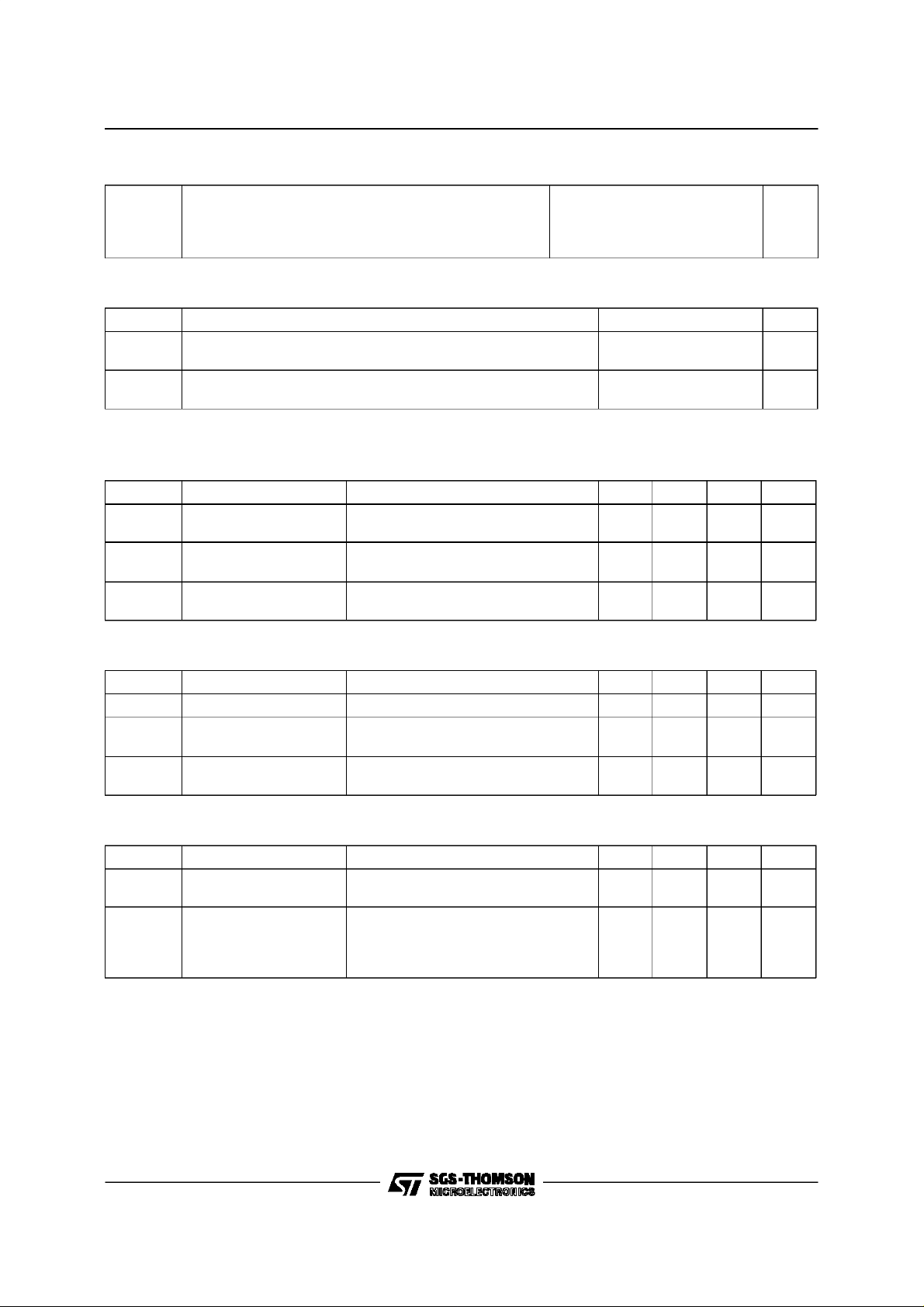
3
2
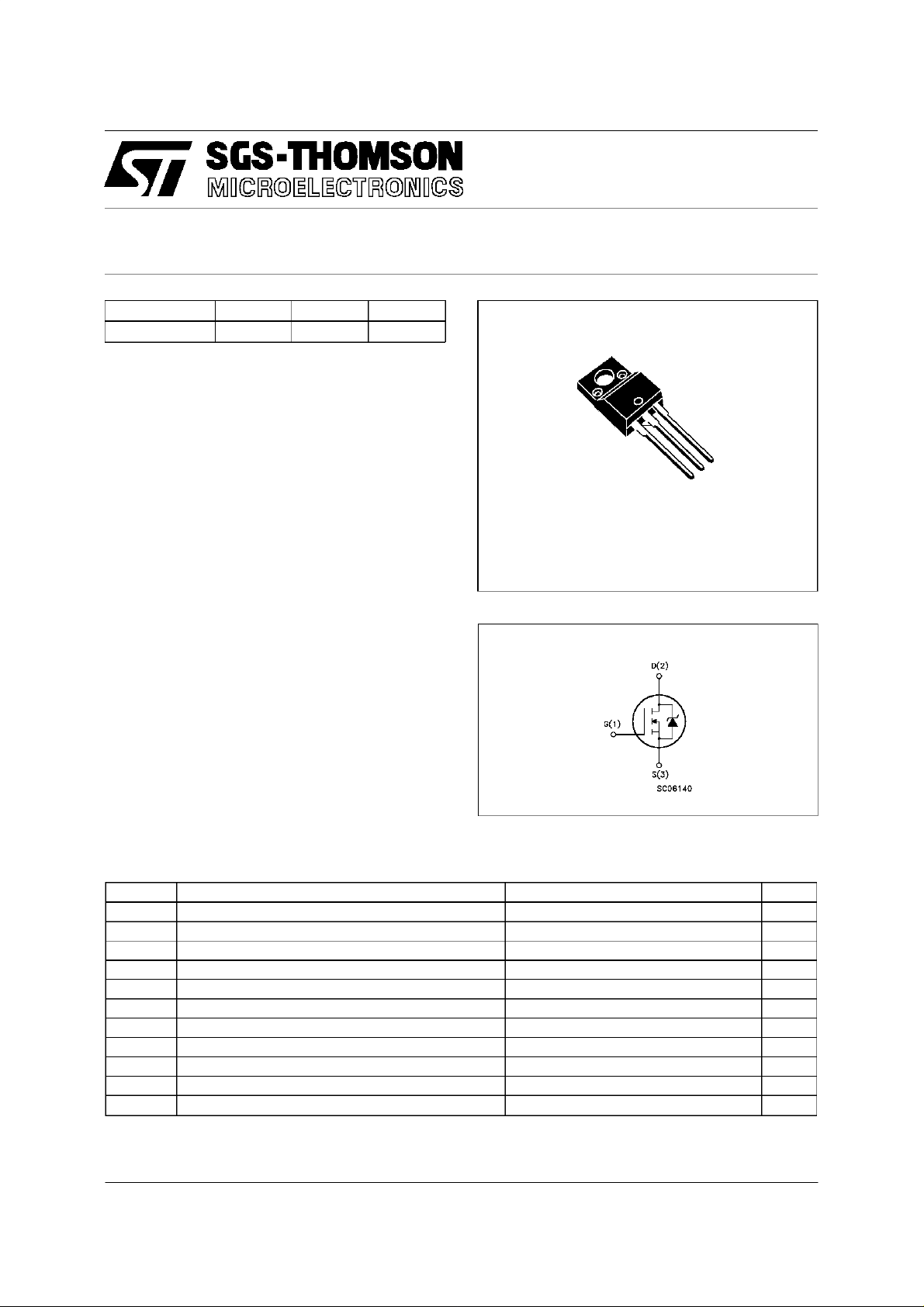
1
TO-220FP
INTERNAL SCHEMATIC DIAGRAM
ABSOLUTE MAXIMUM RATINGS
Symb o l Parame t er Value Uni t
V
V
DGR Drain- gate Voltage (R
V
I
DM
P
V
T
(•) Pulse width limited by safe operating area
October 1997
Drain-source Voltage (VGS=0) 800 V
DS
=20kΩ)
GS
Gate-sourc e Voltage ± 30 V
GS
I
Drain Current (c ont inuo us) a t Tc=25oC2.8A
D
I
Drain Current (c ont inuo us) a t Tc=100oC1.8A
D
800 V
(•) Drain Current (puls ed) 19 A
Total Dissipat i on at Tc=25oC40W
tot
Derat ing Factor 0.32 W/
Insul at ion W ithst and Voltage (DC) 2000 V
ISO
Stora ge Temperatu re -65 to 15 0
stg
T
Max. Operat ing Junc t i on Temperatu r e 150
j
o
C
o
C
o
C
1/5
Page 2
STP5NA80FP
THERMAL DATA
R
thj-case
R
thj-amb
R
thc-sin k
T
AVALANCHE CHARACTERISTICS
Symb o l Para met er Max Val ue Uni t
I
AR
E
Ther mal Resistance Junct ion-cas e Max
Ther mal Resistance Junct ion-ambient Max
Ther mal Resistance Case-s i nk Typ
Maximum Lead Temperat ure For Solder in g P urpos e
l
Avalanche Current, Repetitiv e or Not-Repe t it ive
(pulse width lim i t ed by T
Single Pu lse Avalanc he E nerg y
AS
(starti ng T
=25oC, ID=IAR,VDD=50V)
j
max, δ <1%)
j
3.12
62.5
0.5
300
4.7 A
110 mJ
o
C/W
oC/W
o
C/W
o
C
ELECTRICAL CHARACTERISTICS (T
=25oC unlessotherwise specified)
case
OFF
Symbol Parameter Test Cond ition s Min. Typ. Max. Un it
V
(BR)DSS
Drain-source
= 250 µAVGS=0
I
D
800 V
Break dow n Voltage
I
I
DSS
GSS
Zero Gate Voltage
Drain Current (V
GS
Gat e- bod y Leaka ge
Current (V
DS
=0)
=0)
=MaxRating
V
DS
V
=MaxRating Tc= 100oC
DS
= ± 30 V
V
GS
25
250
± 100 nA
ON (∗)
Symbol Parameter Test Cond ition s Min. Typ. Max. Un it
V
GS(th )
R
DS(on)
Gat e Thre shold Volt age
St at ic Drain-source On
V
DS=VGSID
=250µA
VGS= 10V ID= 2.5 A 1.8 2.4 Ω
2.25 3 3.75 V
Resistance
I
D(on)
On State Drain Current VDS>I
D(on)xRDS(on)max
4.7 A
VGS=10V
DYNAMIC
Symbol Parameter Test Cond ition s Min. Typ. Max. Un it
g
(∗)Forward
fs
Tr ansc on ductance
C
C
C
Input Capac it an ce
iss
Out put Capac itance
oss
ReverseTransfer
rss
Capacit a nc e
VDS>I
D(on)xRDS(on)maxID
=2.5A 2.7 5.2 S
VDS=25V f=1MHz VGS= 0 1250
140
35
1700
190
50
µA
µA
pF
pF
pF
2/5
Page 3

STP5NA80FP
ELECTRICAL CHARACTERISTICS (continued)
SWITCHINGON
Symbol Parameter Test Cond ition s Min. Typ. Max. Un it
t
d(on)
Q
Q
Q
Turn-on Time
Rise Time
t
r
Tot al Gat e Charge
g
Gate-Source Charge
gs
Gat e- Drain Charge
gd
VDD=400V ID=2.5A
=47 Ω VGS=10V
R
G
VDD=480V ID=3A VGS=10V 55
SWITCHINGOFF
Symbol Parameter Test Cond ition s Min. Typ. Max. Un it
t
r(Voff)
t
Off -voltage Rise Time
t
Fall T ime
f
Cross-over T ime
c
VDD=640V ID=5A
=47 Ω VGS=10V
R
G
(see test cir cuit, figure 5)
SOURCE DRAIN DIODE
Symbol Parameter Test Cond ition s Min. Typ. Max. Un it
I
SD
I
SDM
V
SD
t
Q
I
RRM
(∗) Pulsed: Pulse duration =300 µs, duty cycle1.5 %
(•) Pulse width limited by safe operating area
Source-drain Current
(•)
Source-drain Current
(pulsed)
(∗)ForwardOnVoltage ISD=4.7A VGS=0 1.6 V
Reverse Recovery
rr
Time
Reverse Recovery
rr
= 5 A di/dt = 100 A/µs
I
SD
=100V Tj=150oC
V
DD
(see circuit, figure 5)
Charge
Reverse Recovery
Current
40
10055135
75 nC
8
24
75
25
110
100
35
150
4.7
19
800
15.2
38
ns
ns
nC
nC
ns
ns
ns
A
A
ns
µC
A
3/5
Page 4

STP5NA80FP
TO-220FP MECHANICAL DATA
DIM.
MIN. TYP. MAX. MIN. TYP. MAX.
A 4.4 4.6 0.173 0.181
B 2.5 2.7 0.098 0.106
D 2.5 2.75 0.098 0.108
E 0.45 0.7 0.017 0.027
F 0.75 1 0.030 0.039
F1 1.15 1.7 0.045 0.067
F2 1.15 1.7 0.045 0.067
G 4.95 5.2 0.195 0.204
G1 2.4 2.7 0.094 0.106
H 10 10.4 0.393 0.409
L2 16 0.630
L3 28.6 30.6 1.126 1.204
L4 9.8 10.6 0.385 0.417
L6 15.9 16.4 0.626 0.645
L7 9 9.3 0.354 0.366
Ø 3 3.2 0.118 0.126
mm inch
E
A
D
B
L3
L6
L7
¯
F1
F
G1
H
G
F2
123
L2
L4
4/5
Page 5

STP5NA80FP
Informationfurnished is believed to be accurate and reliable.However, SGS-THOMSONMicroelectronics assumesno responsabilityfor the
consequencesof use of such informationnor for any infringementof patents or other rightsof third parties which may results fromits use.No
license is granted byimplicationor otherwise under anypatentor patentrights ofSGS-THOMSONMicroelectronics.Specificationsmentioned
in this publication are subject tochange without notice.This publicationsupersedes and replacesall informationpreviously supplied.
SGS-THOMSON Microelectronicsproducts arenotauthorizedfor use as criticalcomponentsinlifesupport devices or systems without express
written approvalof SGS-THOMSONMicroelectonics.
1997 SGS-THOMSON Microelectronics - Printedin Italy- All Rights Reserved
Australia- Brazil - Canada- China- France- Germany- Hong Kong - Italy - Japan- Korea -Malaysia - Malta - Morocco -The Netherlands-
Singapore - Spain- Sweden - Switzerland - Taiwan - Thailand- UnitedKingdom- U.S.A
SGS-THOMSON MicroelectronicsGROUP OF COMPANIES
...
5/5
 Loading...