

Page 1
STP55NF03L
N-CHANNEL 30V - 0.01Ω - 55A TO-220
STripFET POWER MOSFET
TYPE
V
DSS
R
DS(on)
I
D
STP55NF03L 30 V <0.013 Ω 55 A
■ TYPICAL RDS(on) = 0.01Ω
■ OPTIMIMIZED FOR HIGH SWITCHING
OPERATIONS
■ LOW GATE CHARGE
■ LOGIC LEVEL GATE DRIVE
DESCRIPTION
This Power MOSFET is the latest development of
STMicroelectronics unique “Single Feature
Size” strip-basedprocess. The resulting transistor shows extremely high packing density for low
on-resistance, rugged avalanche characteristics
and less critical alignment steps therefore a remarkable manufacturing reproducibility.
APPLICATIONS
■ LOW VOLTAGE DC-DC CONVERTERS
■ HIGH CURRENT, HIGHSPEED SWITCHING
■ HIGH EFFICIENCY SWITCHING CIRCUITS
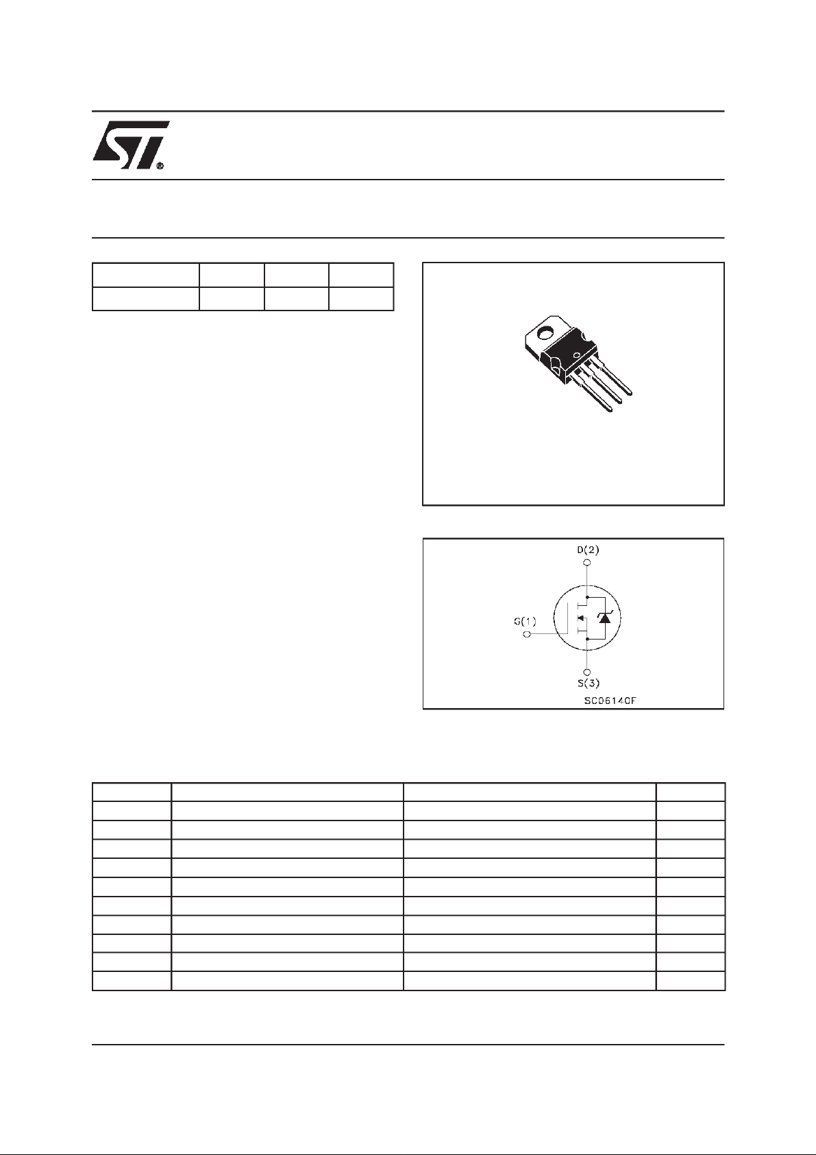
3
2
1
TO-220
INTERNAL SCHEMATIC DIAGRAM
ABSOLUTE MAXIMUM RATINGS
Symbol Parameter Value Unit
V
DS
V
DGR
V
GS
I
D
I
D
(•)
I
DM
P
tot
T
stg
T
j
(•)Pulse width limited by safe operating area.
Drain-source Voltage (VGS=0) 30 V
Drain-gate Voltage (RGS=20kΩ)
30 V
Gate- source Voltage ±15 V
Drain Current (continuos) at TC=25°C
55 A
Drain Current (continuos) at TC= 100°C39 A
Drain Current (pulsed) 220 A
TotalDissipation at TC=25°C
80 W
Derating Factor 0.53 W/°C
Storage Temperature –60 to 175 °C
Max. Operating Junction Temperature 175 °C
1/8February 2001
Page 2
STP55NF03L
THERMAL DATA
R
thj-case
R
thj-amb
R
thc-sink
T
j
Thermal Resistance Junction-case
Thermal Resistance Junction-ambient
Thermal Resistance Case-sink
Maximum Lead Temperature For Soldering Purpose
Max
Max
Typ
1.875
62.5
0.5
300
°C/W
°C/W
°C/W
°C
ELECTRICAL CHARACTERISTICS (T
=25°C unless otherwise specified)
case
OFF
Symbol Parameter Test Conditions Min. Typ. Max. Unit
ON
V
(BR)DSS
I
DSS
I
GSS
(*)
Drain-source
Breakdown Voltage
Zero Gate Voltage
Drain Current (V
GS
Gate-body Leakage
Current (V
DS
=0)
=0)
ID= 250 µAVGS=0 30 V
V
= Max Rating
DS
=Max Rating TC= 125 °C
V
DS
V
= ±15 V ±100 nA
GS
1
10
Symbol Parameter Test Conditions Min. Typ. Max. Unit
V
GS(th)
R
DS(on)
I
D(on)
Gate Threshold Voltage VDS=V
Static Drain-source On Resis-
tance
VGS=10V ID= 27.5 A
= 4.5 V ID= 27.5 A
V
GS
On State Drain Current VDS>I
VGS=10V
GS
D(on)xRDS(on)max
ID= 250 µA1 V
0.01
0.013
0.013
0.020
55 A
DYNAMIC
Symbol Parameter Test Conditions Min. Typ. Max. Unit
(*)
g
fs
Forward Transconductance VDS>I
ID=27.5 A
D(on)xRDS(on)max
30 S
µA
µA
Ω
Ω
2/8
C
iss
C
oss
C
rss
Input Capacitance
Output Capacitance
Reverse Transfer
Capacitances
= 25V f = 1 MHz VGS= 0 1265
V
DS
435
115
pF
pF
pF
Page 3
STP55NF03L
ELECTRICAL CHARACTERISTICS (continued)
SWITCHING ON
Symbol Parameter Test Conditions Min. Typ. Max. Unit
t
d(on)
t
Turn-on DelayTime Rise Time VDD=15V ID= 27.5 A
= 4.7 Ω VGS= 4.5 V
r
R
G
(see test circuit, Figure 3)
28
400
ns
ns
Q
g
Q
gs
Q
gd
Total Gate Charge
Gate-Source Charge
Gate-Drain Charge
=24V ID=55A VGS=4.5V 20
V
DD
7
27 nC
10
SWITCHING OFF
Symbol Parameter Test Conditions Min. Typ. Max. Unit
t
d(off)
t
turn-off Delay Time
f
Fall Time
VDD=15V ID= 27.5 A
= 4.7 Ω VGS= 4.5 V
R
G
25
50
(see test circuit, Figure 3)
SOURCE DRAIN DIODE
Symbol Parameter Test Conditions Min. Typ. Max. Unit
I
SD
I
SDM
V
SD
t
rr
Q
rr
I
RRM
(*)Pulsed: Pulse duration = 300 µs, duty cycle 1.5 %.
(•)Pulse width limitedby safe operating area.
Source-drain Current
(•)
Source-drain Current (pulsed)
55
220
(*) Forward On Voltage ISD=55A VGS= 0 1.3 V
Reverse Recovery Time
Reverse Recovery Charge
Reverse Recovery Current
=55 A di/dt = 100A/µs
I
SD
=30V Tj= 150 °C
V
DD
(see test circuit, Figure 5)
70
160
4.5
nC
nC
ns
ns
A
A
ns
nC
A
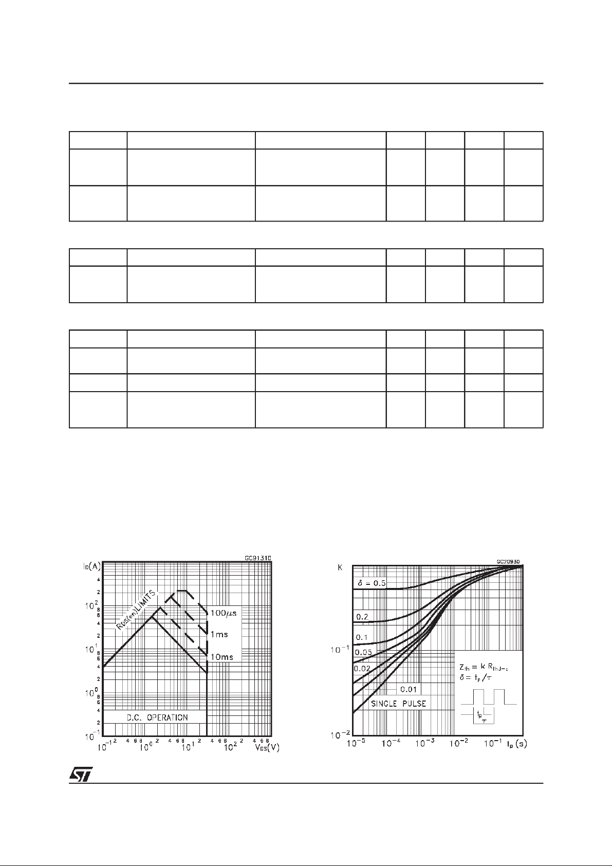
Thermal ImpedanceSafe Operating Area
3/8
Page 4

STP55NF03L
Output Characteristics Transfer Characteristics
Transconductance Static Drain-source On Resistance
Gate Charge vs Gate-source Voltage Capacitance Variations
4/8
Page 5

STP55NF03L
Normalized Gate Threshold Voltage vs
Temperature
Source-drain Diode Forward Characteristics
Normalized On Resistance vs Temperature
Normalized Breakdown Voltage vs Temperature
5/8
Page 6

STP55NF03L
Fig. 1: Unclamped Inductive Load Test Circuit Fig. 2: UnclampedInductive Waveform
Fig. 1: Unclamped Inductive Load Test Circuit
Fig. 3:SwitchingTimesTestCircuits ForResistive
Load
Fig. 5: Test Circuit For Inductive Load Switching
And Diode Recovery Times
Fig. 4: Gate Charge test Circuit
6/8
Page 7

TO-220 MECHANICALDATA
STP55NF03L
DIM.
MIN. TYP. MAX. MIN. TYP. MAX.
A 4.40 4.60 0.173 0.181
C 1.23 1.32 0.048 0.051
D 2.40 2.72 0.094 0.107
D1 1.27 0.050
E 0.49 0.70 0.019 0.027
F 0.61 0.88 0.024 0.034
F1 1.14 1.70 0.044 0.067
F2 1.14 1.70 0.044 0.067
G 4.95 5.15 0.194 0.203
G1 2.4 2.7 0.094 0.106
H2 10.0 10.40 0.393 0.409
L2 16.4 0.645
L4 13.0 14.0 0.511 0.551
L5 2.65 2.95 0.104 0.116
L6 15.25 15.75 0.600 0.620
L7 6.2 6.6 0.244 0.260
L9 3.5 3.93 0.137 0.154
DIA. 3.75 3.85 0.147 0.151
mm inch
E
A
L4
D
F2
F1
G1
H2
G
F
C
D1
L2
Dia.
L5
L7
L6
L9
P011C
7/8
Page 8

STP55NF03L
Information furnished is believed tobe accurate and reliable. However, STMicroelectronics assumes no responsibility for the consequences
of use ofsuch information nor for any infringement ofpatents or other rights ofthird parties which may result from itsuse. No licenseisgranted
by implication or otherwise under any patent or patent rights of STMicroelectronics. Specifications mentioned in this publication are subject
to change without notice. This publication supersedes and replaces all information previously supplied. STMicroelectronics products are not
authorized for use as critical components in lifesupport devices or systems without express written approval of STMicroelectronics.
The ST logo is registered trademark of STMicroelectronics
2001 STMicroelectronics - All Rights Reserved
All other names are the property of their respective owners.
Australia - Brazil - China - Finland - France - Germany - Hong Kong - India - Italy - Japan - Malaysia - Malta - Morocco -
Singapore - Spain - Sweden -Switzerland - United Kingdom - U.S.A.
STMicroelectronics GROUP OF COMPANIES
http://www.st.com
8/8
 Loading...