

Page 1
STP55NE06
STP55NE06FP
N - CHANNEL ENHANCEMENT MODE
” SINGLE FEATURE SIZE ” POWER MOSFET
TYPE V
STP55NE06
STP55NE06FP
■ TYPICALR
■ EXCEPTIONAL dv/dt CAPABILITY
■ 100% AVALANCHETESTED
■ LOW GATE CHARGE 100
■ HIGH dv/dt CAPABILITY
■ APPLICATIONORIENTED
DS(on)
DSS
60 V
60 V
=0.019 Ω
R
DS(on)
<0.022Ω
<0.022Ω
o
C
I
D
55 A
30 A
CHARACTERIZATION
DESCRIPTION
This Power Mosfet is the latest development of
SGS-THOMSON unique ”Single Feature Size”
strip-based process. The resulting transistor
shows extremelyhigh packing density for low onresistance, rugged avalance characteristics and
less critical alignment steps therefore a remarkable manufacturingreproducibility.
APPLICATIONS
■ DC MOTOR CONTROL
■ DC-DC& DC-AC CONVERTERS
■ SYNCHRONOUS RECTIFICATION
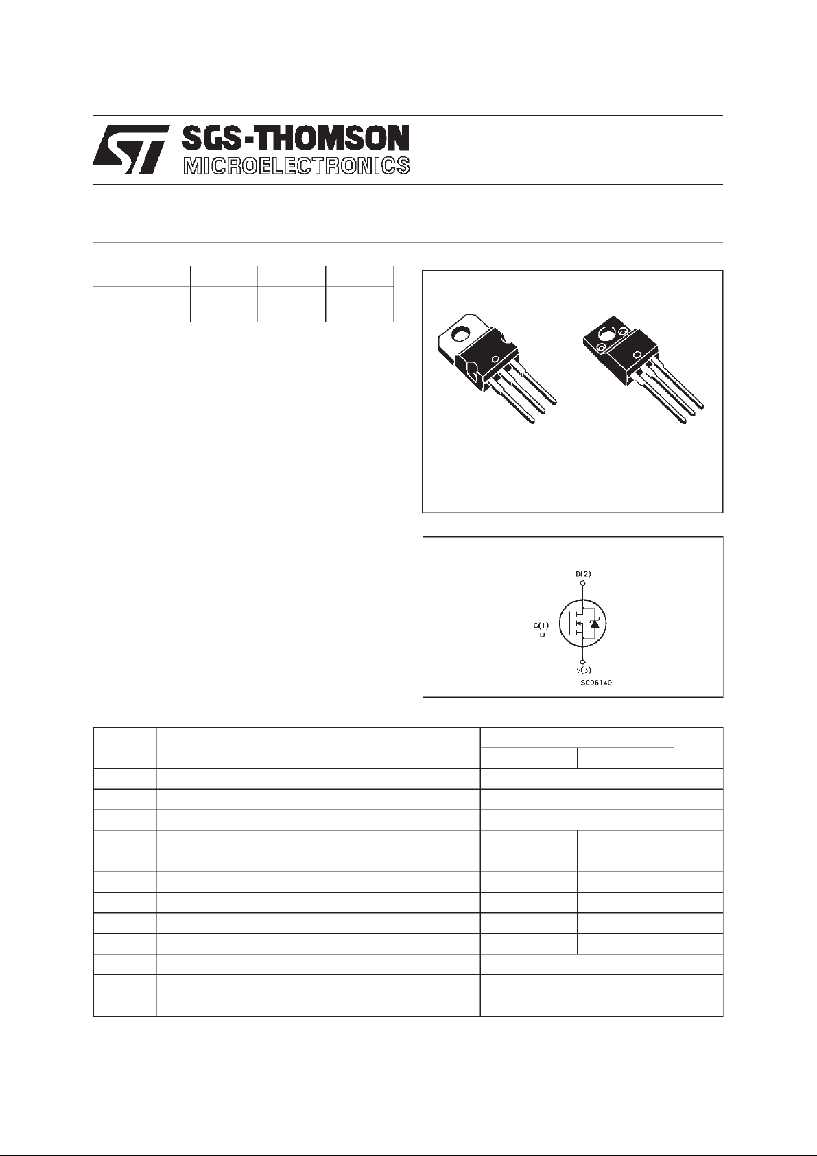
3
2
1
TO-220 TO-220FP
INTERNAL SCHEMATIC DIAGRAM
3
2
1
ABSOLUTE MAXIMUM RATINGS
Symb o l Para meter Value Uni t
STP 55NE06 STP55 NE06F P
V
V
V
I
DM
P
V
dv/ dt Peak Diode Recov ery vo lt age sl ope 7 V/ns
T
(•) Pulsewidth limitedby safe operating area (1)ISD≤ 55 A,di/dt ≤ 300 A/µs, VDD≤ V
January 1998
Drain-source Voltage (VGS=0) 60 V
DS
Drain- gate Voltage ( RGS=20kΩ)
DGR
Gat e- source Volt age ± 20 V
GS
I
Drain Current (c on t in uous) at Tc=25oC5530A
D
I
Drain Current (c on t in uous) at Tc=100oC3921A
D
60 V
(•) Dr a in Curr ent (pul sed) 220 220 A
Tot al Dissip at i on at Tc=25oC13035W
tot
Derat in g F actor 0.96 0.27 W/
Ins ulation With st and Voltage (DC) 2000 V
ISO
Sto rage T emperat ure -65 to 17 5
stg
T
Max. Oper at in g Junc t io n Temperatur e 175
j
(BR)DSS,Tj≤TJMAX
o
C
o
C
o
C
1/9
Page 2
STP55NE06/FP
THERMAL DATA
TO - 2 20 TO-220FP
R
thj-case
R
thj-amb
R
thc-sin k
T
AVALANCHE CHARACTERISTICS
Symbol Paramet e r Max Va lu e Uni t
I
AR
E
Ther mal Resist ance Junction- case Max 1.15 4.28
Ther mal Resist ance Junction- ambient Max
Ther mal Resist ance Case-sink Ty p
Maximum Lead Tempera t ure For Sold ering Purpose
l
Avalanche Current, Repetit i v e or Not-Repetitive
(pulse w idth limited by T
Single Pulse Avalanche Energy
AS
(starting T
=25oC, ID=IAR,VDD=25V)
j
max, δ <1%)
j
62.5
0.5
300
55 A
200 mJ
o
C/W
o
C/W
o
C/W
o
C
ELECTRICAL CHARACTERISTICS (T
=25oC unlessotherwise specified)
case
OFF
Symbol Parameter Test Cond itions Min. Typ. Max. Unit
V
(BR)DSS
Drain-source
=250µAVGS=0
I
D
60 V
Breakdown Voltage
I
DSS
I
GSS
Zer o Gate Vo lt age
Drain Cur re nt (V
GS
Gat e-body Leakage
Current (V
DS
=0)
=0)
=MaxRating
V
DS
V
=MaxRating Tc=125
DS
o
C
= ± 20 V
V
GS
1
10
± 100 nA
ON (∗)
Symbol Parameter Test Cond itions Min. Typ. Max. Unit
V
GS(th )
Gate Threshold
V
DS=VGSID
=250µA
234V
Voltage
R
DS(on)
Stati c Drain-so urce On
VGS=10V ID= 27.5 A 0.019 0.022 Ω
Resistance
I
D(on)
On State Drain Cu rr e nt VDS>I
D(on)xRDS(on)max
55 A
VGS=10V
DYNAMIC
Symbol Parameter Test Cond itions Min. Typ. Max. Unit
g
(∗)Forward
fs
Tr ansconductance
C
C
C
Input Capaci t ance
iss
Out put Capa citance
oss
Reverse Transfer
rss
Capa cit an c e
VDS>I
D(on)xRDS(on)maxID
=27. 5 A 25 35 S
VDS=25V f=1MHz VGS= 0 3050
380
100
4000
500
130
µA
µA
pF
pF
pF
2/9
Page 3
STP55NE06/FP
ELECTRICAL CHARACTERISTICS (continued)
SWITCHINGON
Symbol Parameter Test Cond itions Min. Typ. Max. Unit
t
d(on)
t
Q
Q
Q
SWITCHINGOFF
Symbol Parameter Test Cond itions Min. Typ. Max. Unit
t
r(Voff)
t
SOURCE DRAIN DIODE
Symbol Parameter Test Cond itions Min. Typ. Max. Unit
I
SD
I
SDM
V
SD
t
Q
I
RRM
(∗) Pulsed: Pulse duration =300 µs, duty cycle 1.5 %
(•) Pulse widthlimited by safe operating area
r
Turn-on Time
Rise Tim e
VDD=30V ID= 27.5 A
R
=4.7 W VGS=10V
G
30
12040160
(see test circuit, figure 3)
Total Gate Charge
g
Gat e-Sourc e Charge
gs
Gate-Drain Charge
gd
Of f - voltage Rise T im e
t
Fall Time
f
Cross-over Time
c
Source-drain Current
(•)
Source-drain Current
VDD=48V ID=55A VGS=10V 80
13
25
VDD=48V ID=55A
=4.7 Ω VGS=10V
R
G
(see test circuit, figure 5)
20
50
75
105 nC
30
70
100
55
220
(pulsed)
(∗) For ward O n Vo lt age ISD=60A VGS=0 1.5 V
Reverse Recover y
rr
Time
Reverse Recover y
rr
= 55 A di/dt = 100 A /µ s
I
SD
=30V Tj=150oC
V
DD
(see test circuit, figure 5)
110
430
Charge
Reverse Recover y
7.5
Current
ns
ns
nC
nC
ns
ns
ns
A
A
ns
µC
A
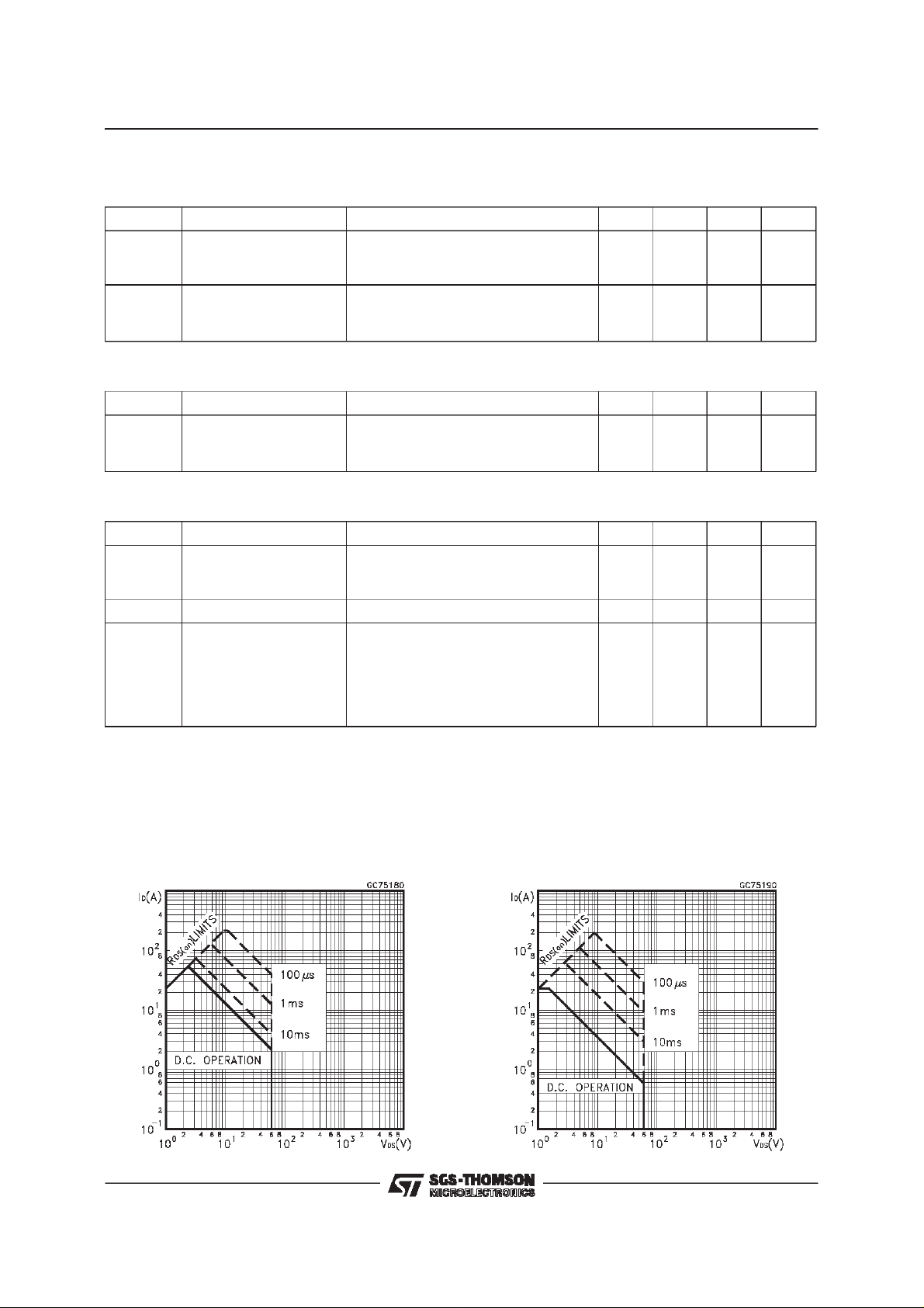
Safe Operating Areafor TO-220 Safe Operating Area for TO-220FP
3/9
Page 4

STP55NE06/FP
ThermalImpedance for TO-220
OutputCharacteristics
ThermalImpedance forTO-220FP
TransferCharacteristics
Transconductance
4/9
StaticDrain-sourceOn Resistance
Page 5

STP55NE06/FP
GateCharge vs Gate-sourceVoltage
Normalized GateThresholdVoltage vs
Temperature
CapacitanceVariations
Normalized On Resistancevs Temperature
Source-drainDiode Forward Characteristics
5/9
Page 6

STP55NE06/FP
Fig. 1: UnclampedInductiveLoad Test Circuit
Fig. 3: Switching Times Test CircuitsFor
ResistiveLoad
Fig. 2: UnclampedInductive Waveform
Fig. 4: Gate Charge test Circuit
Fig. 5: Test Circuit For Inductive Load Switching
And Diode RecoveryTimes
6/9
Page 7

TO-220 MECHANICALDATA
STP55NE06/FP
DIM.
MIN. TYP. MAX. MIN. TYP. MAX.
A 4.40 4.60 0.173 0.181
C 1.23 1.32 0.048 0.051
D 2.40 2.72 0.094 0.107
D1 1.27 0.050
E 0.49 0.70 0.019 0.027
F 0.61 0.88 0.024 0.034
F1 1.14 1.70 0.044 0.067
F2 1.14 1.70 0.044 0.067
G 4.95 5.15 0.194 0.203
G1 2.4 2.7 0.094 0.106
H2 10.0 10.40 0.393 0.409
L2 16.4 0.645
L4 13.0 14.0 0.511 0.551
L5 2.65 2.95 0.104 0.116
L6 15.25 15.75 0.600 0.620
L7 6.2 6.6 0.244 0.260
L9 3.5 3.93 0.137 0.154
DIA. 3.75 3.85 0.147 0.151
mm inch
E
A
L4
D
F2
F1
G1
H2
G
F
C
D1
L2
Dia.
L5
L7
L6
L9
P011C
7/9
Page 8

STP55NE06/FP
TO-220FP MECHANICALDATA
DIM.
MIN. TYP. MAX. MIN. TYP. MAX.
A 4.4 4.6 0.173 0.181
B 2.5 2.7 0.098 0.106
D 2.5 2.75 0.098 0.108
E 0.45 0.7 0.017 0.027
F 0.75 1 0.030 0.039
F1 1.15 1.7 0.045 0.067
F2 1.15 1.7 0.045 0.067
G 4.95 5.2 0.195 0.204
G1 2.4 2.7 0.094 0.106
H 10 10.4 0.393 0.409
L2 16 0.630
L3 28.6 30.6 1.126 1.204
L4 9.8 10.6 0.385 0.417
L6 15.9 16.4 0.626 0.645
L7 9 9.3 0.354 0.366
Ø 3 3.2 0.118 0.126
mm inch
E
A
D
B
L3
L6
L7
¯
F1
F
G1
H
G
F2
123
L2
L4
8/9
Page 9

STP55NE06/FP
Information furnished is believedto be accurateand reliable. However,SGS-THOMSON Microelectronics assumes no responsability for the
consequencesof use of such information nor for any infringement ofpatents or otherrights of third parties which may resultsfrom its use. No
licenseis granted by implicationor otherwise underany patentor patentrights ofSGS-THOMSONMicroelectronics. Specificationsmentioned
in this publicationare subject to change without notice. This publication supersedes and replaces all information previously supplied.
SGS-THOMSONMicroelectronics productsare notauthorized for useascriticalcomponents in life supportdevices or systems withoutexpress
writtenapproval of SGS-THOMSONMicroelectonics.
1997 SGS-THOMSONMicroelectronics - Printedin Italy- AllRights Reserved
Australia- Brazil- Canada - China - France - Germany - Italy- Japan - Korea -Malaysia - Malta- Morocco - The Netherlands -
Singapore- Spain- Sweden - Switzerland- Taiwan - Thailand - United Kingdom- U.S.A
SGS-THOMSONMicroelectronicsGROUP OF COMPANIES
...
9/9
 Loading...