

Page 1
STP50NE10
N - CHANNEL 100V - 0.021Ω - 50A TO-220
STripFET POWER MOSFET
TYPE V
DSS
R
DS(on)
I
D
ST P50NE10 100 V <0 . 027 Ω 50 A
■ TYPICALR
■ EXCEPTIONALdv/dtCAPABILITY
■ 100%AVALANCHETESTED
■ LOW GATE CHARGE AT100
■ APPLICATIONORIENTED
DS(on)
= 0.021 Ω
o
C
CHARACTERIZATION
DESCRIPTION
This PowerMOSFET is the latest developmentof
STMicroelectronics unique ”Single Feature
Size” strip-based process. The resulting
transistor shows extremely high packing density
for low on-resistance, rugged avalanche
characteristics and less critical alignment steps
therefore a remarkable manufacturing
reproducibility.
APPLICATIONS
■ HIGHCURRENT, HIGH SPEED SWITCHING
■ SOLENOIDAND RELAYDRIVERS
■ MOTORCONTROL, AUDIO AMPLIFIERS
■ DC-DC& DC-ACCONVERTERS
■ AUTOMOTIVEENVIRONMENT
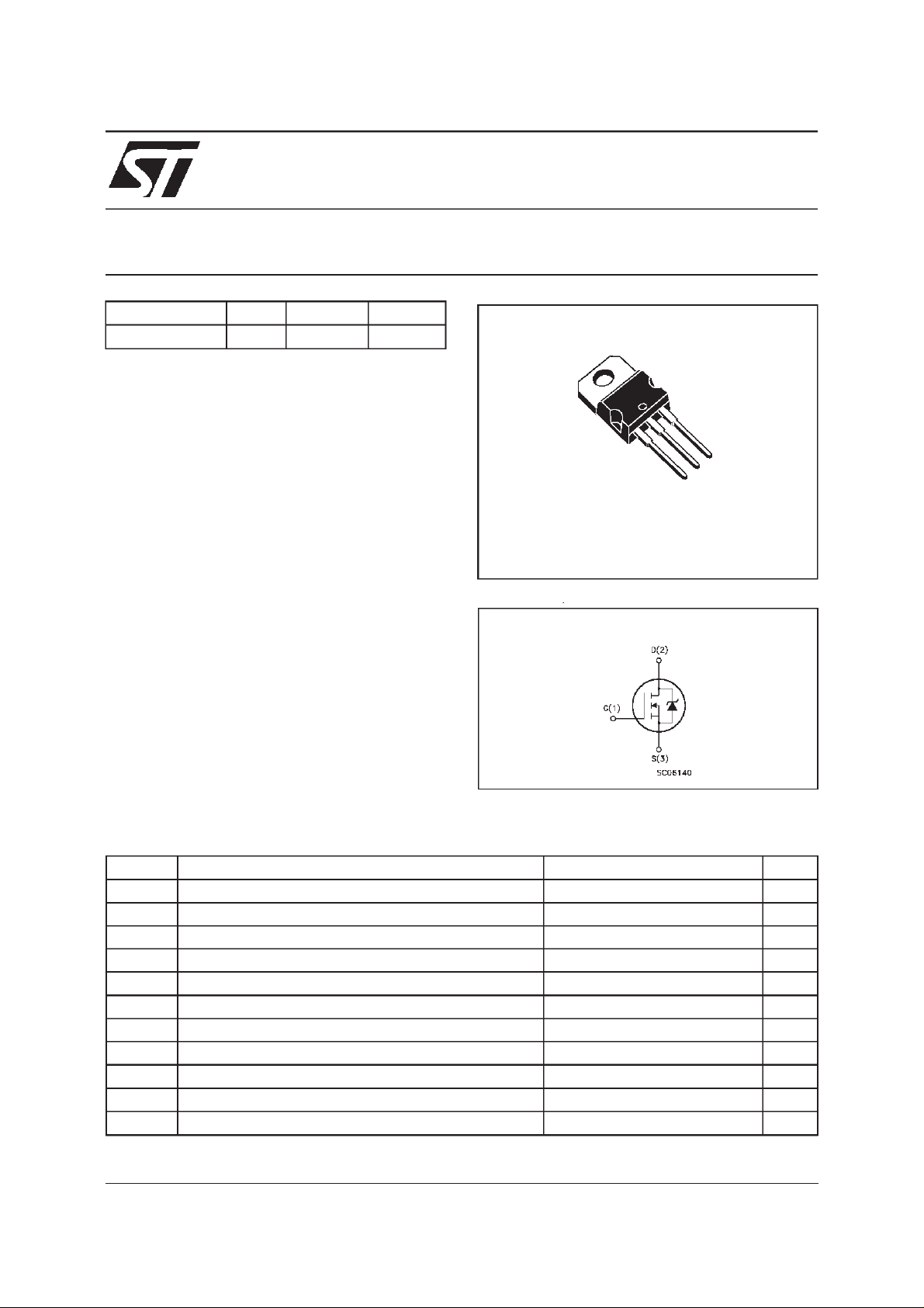
3
2
1
TO-220
INTERNAL SCHEMATIC DIAGRAM
ABSOLUTE MAXIMUM RATINGS
Symbol Parameter Value Unit
V
V
V
I
DM
P
dv/dt (
T
(•) Pulsewidth limited by safeoperating area (1)ISD≤ 50 A, di/dt ≤ 300 A/µs, VDD≤ V
April 1999
Dra in- sour c e Vol t age (VGS= 0) 100 V
DS
Dra in- gate Voltage (RGS=20kΩ) 100 V
DGR
Gat e-source Voltage ± 20 V
GS
I
Dra in Current ( continuous) at Tc=25oC50A
D
I
Dra in Current ( continuous) at Tc=100oC35A
D
(•) D rain Cu rr ent ( p uls ed ) 200 A
Tot al Dissipation at Tc=25oC 150 W
tot
Derating Factor 1 W/
1) Peak Diode Re c overy v olt age slope 6 V/ ns
St orage Tem pe r at ure -65 to 175
stg
T
Max. Operat ing Junct ion Temperature 175
j
(BR)DSS,Tj≤TJMAX
o
C
o
C
o
C
1/8
Page 2
STP50NE10
THERMAL DATA
R
thj-case
Rthj-amb
R
thc-sink
T
AVALANCHE CHARACTERISTICS
Symbol Parameter Max Value Un it
I
AR
E
Ther mal Resistanc e Junct ion-case Max
Ther mal Resistanc e Junct ion-ambient Max
Ther mal Resistanc e Case-sink Ty p
Maximum L ead Tempera tur e For Solder ing Purp ose
l
Avalanche Current, Repetitive or Not-Repetitive
(pulse width limited by T
Single Pulse A valanche Energy
AS
(starting T
=25oC, ID=IAR,VDD=50V)
j
max)
j
1
62.5
0.5
300
50 A
300 mJ
o
C/W
oC/W
o
C/W
o
C
ELECTRICAL CHARACTERISTICS
=25oC unless otherwisespecified)
(T
case
OFF
Symbol Parameter Test Conditions Min. Typ. Max. Unit
V
(BR)DSS
Drain-source
ID=250µAVGS= 0 100 V
Break dow n Voltage
I
DSS
I
GSS
Zero Gate Voltage
Drain Current (V
GS
Gat e- bod y Leakage
Current (V
DS
=0)
=0)
V
=MaxRating
DS
=MaxRating Tc= 125oC
V
DS
V
=± 20 V
GS
1
10
100 nA
±
ON(∗)
Symbol Parameter Test Conditions Min. Typ. Max. Unit
V
GS(th)
R
DS(on)
Gate Threshold Volt age VDS=VGSID= 250 µ A 234V
Sta t ic Drain-sour ce On
VGS=10V ID= 25 A 0.021 0.027
Resistance
I
D(on)
On State Drain Current VDS>I
D(on)xRDS(on )max
50 A
VGS=10V
DYNAMIC
Symbol Parameter Test Conditions Min. Typ. Max. Unit
g
(∗)Forward
fs
Tr ansc on duc tance
C
C
C
Input Capacitance
iss
Out put Capacitance
oss
Reverse Transfer
rss
Capacit a nc e
VDS>I
D(on)xRDS(on )maxID
=25 A 20 35 S
VDS=25V f=1MHz VGS= 0 4350
500
175
6000
675
238
µ
µA
Ω
pF
pF
pF
A
2/8
Page 3
STP50NE10
ELECTRICAL CHARACTERISTICS
(continued)
SWITCHING ON
Symbol Parameter Test Conditions Min. Typ. Max. Unit
t
d(on)
t
r
Turn-on Time
Rise Time
VDD=50V ID=25A
R
G
=4.7
Ω
VGS=10V
25
10034135
(see test circuit, figure 3)
Q
Q
Q
Tot al Gate Charge
g
Gat e- Source Char g e
gs
Gate-Drain Charg e
gd
VDD=80V ID=50A VGS= 10 V 123
24
47
166 nC
SWITCHING OFF
Symbol Parameter Test Conditions Min. Typ. Max. Unit
t
r(Voff)
t
t
Off-volt age Rise Tim e
Fall T ime
f
Cross-over Time
c
VDD=80V ID=50A
=4.7 Ω VGS=10V
R
G
(see test circuit, figure 5)
45
35
65
61
48
88
SOURCEDRAIN DIODE
Symbol Parameter Test Conditions Min. Typ. Max. Unit
I
SD
I
SDM
V
SD
t
Q
I
RRM
(∗) Pulsed:Pulse duration = 300µs, duty cycle 1.5%
(•) Pulse width limited by safeoperating area
Source-drain Current
(•)
Source-drain Current
50
200
(pulsed)
(∗)ForwardOnVoltage ISD=50A VGS=0 1.5 V
Reverse Recovery
rr
Time
Reverse Recovery
rr
ISD= 50 A di/dt = 100 A /µs
=30V Tj= 150oC
V
DD
(see test circuit, figure 5)
155
815
210
1100
Charge
Reverse Recovery
10.5
15
Current
ns
ns
nC
nC
ns
ns
ns
A
A
ns
nC
A
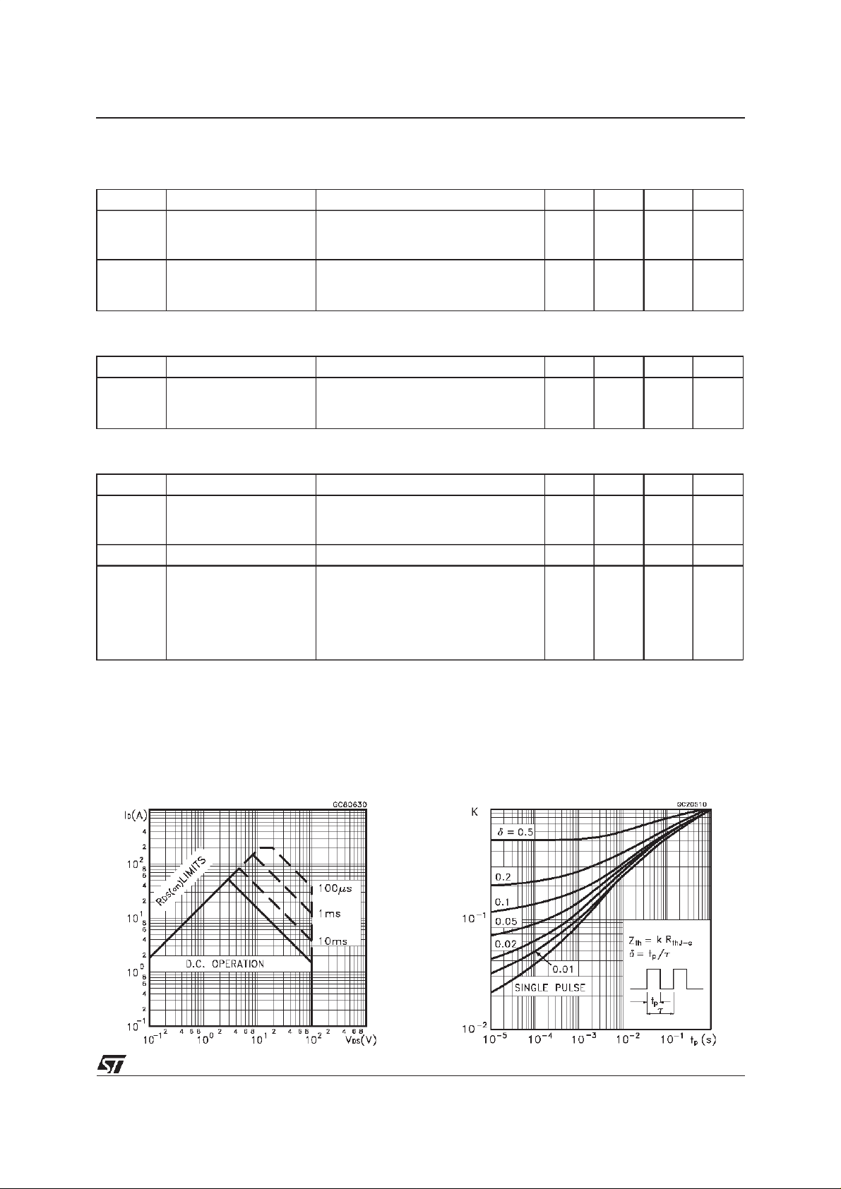
SafeOperating Area ThermalImpedance
3/8
Page 4

STP50NE10
OutputCharacteristics
Transconductance
TransferCharacteristics
Static Drain-sourceOn Resistance
Gate Charge vs Gate-sourceVoltage
4/8
CapacitanceVariations
Page 5

STP50NE10
NormalizedGate ThresholdVoltage vs
Temperature
Source-drainDiode Forward Characteristics
NormalizedOn Resistancevs Temperature
5/8
Page 6

STP50NE10
Fig. 1:
UnclampedInductiveLoad TestCircuit
Fig. 3: SwitchingTimes Test Circuits For
ResistiveLoad
Fig. 2:
UnclampedInductiveWaveform
Fig. 4: Gate Charge test Circuit
Fig. 5:
Test Circuit For InductiveLoad Switching
And Diode Recovery Times
6/8
Page 7

TO-220 MECHANICALDATA
STP50NE10
DIM.
MIN. TYP. MAX. MIN. TYP. MAX.
A 4.40 4.60 0.173 0.181
C 1.23 1.32 0.048 0.051
D 2.40 2.72 0.094 0.107
D1 1.27 0.050
E 0.49 0.70 0.019 0.027
F 0.61 0.88 0.024 0.034
F1 1.14 1.70 0.044 0.067
F2 1.14 1.70 0.044 0.067
G 4.95 5.15 0.194 0.203
G1 2.4 2.7 0.094 0.106
H2 10.0 10.40 0.393 0.409
L2 16.4 0.645
L4 13.0 14.0 0.511 0.551
L5 2.65 2.95 0.104 0.116
L6 15.25 15.75 0.600 0.620
L7 6.2 6.6 0.244 0.260
L9 3.5 3.93 0.137 0.154
DIA. 3.75 3.85 0.147 0.151
mm inch
E
A
L4
D
F2
F1
G1
H2
G
F
P011C
C
D1
L2
Dia.
L5
L7
L6
L9
7/8
Page 8

STP50NE10
Information furnished is believed tobeaccurateand reliable. However, STMicroelectronics assumesno responsibility for the consequences
of use of such information nor for any infringement of patents or other rights of third parties which may resultfrom its use. No license is
granted by implication or otherwise under any patent or patent rights of STMicroelectronics. Specificationmentioned in this publicationare
subjecttochange without notice.Thispublication supersedesand replacesall information previouslysupplied.STMicroelectronics products
are not authorizedfor useas critical components in lifesupport devices or systems without express written approval of STMicroelectronics.
The STlogo is a trademark of STMicroelectronics
1999 STMicroelectronics – Printed in Italy – All Rights Reserved
STMicroelectronics GROUP OF COMPANIES
Australia - Brazil - Canada - China -France - Germany - Italy- Japan- Korea- Malaysia - Malta - Mexico - Morocco - The Netherlands -
8/8
Singapore - Spain - Sweden - Switzerland - Taiwan- Thailand - UnitedKingdom - U.S.A.
http://www.st.com
.
 Loading...