

Page 1
STP50NE08
N - CHANNEL ENHANCEMENT MODE
” SINGLE FEATURE SIZE ” POWER MOSFET
TYPE V
DSS
R
DS(on)
I
D
STP50NE08 80 V <0.024 Ω 50 A
■ TYPICALR
■ EXCEPTIONAL dv/dt CAPABILITY
■ 100% AVALANCHETESTED
■ LOW GATE CHARGE AT100
■ APPLICATIONORIENTED
DS(on)
=0.020 Ω
o
C
CHARACTERIZATION
DESCRIPTION
This Power MOSFET is the latest development of
SGS-THOMSON unique ”Single Feature Size”
strip-based process. The resulting transistor
shows extremely high packing density for low
on-resistance, rugged avalanche characteristics
and less critical alignment steps therefore a
remarkablemanufacturingreproducibility.
APPLICATIONS
■ HIGH CURRENT, HIGH SPEEDSWITCHING
■ SOLENOIDANDRELAY DRIVERS
■ MOTORCONTROL, AUDIOAMPLIFIERS
■ DC-DC& DC-AC CONVERTERS
■ AUTOMOTIVE ENVIRONMENT(INJECTION,
ABS, AIR-BAG,LAMPDRIVERS,Etc.)
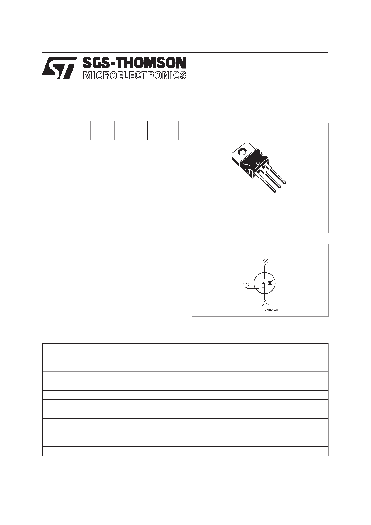
3
2
1
TO-220
INTERNAL SCHEMATIC DIAGRAM
ABSOLUTE MAXIMUM RATINGS
Symb o l Para meter Value Uni t
V
V
V
I
DM
P
dv/dt (
T
(•) Pulsewidth limited by safe operating area (1)ISD≤ 50 A,di/dt ≤ 300A/µs, VDD≤ V
March 1998
Drain-source Voltage (VGS=0) 80 V
DS
Drain- gate Voltage ( RGS=20kΩ)
DGR
Gat e- sourc e Volt age ± 20 V
GS
I
Drain Current (c on t in uous) at Tc=25oC50A
D
I
Drain Current (c on t in uous) at Tc=100oC35A
D
80 V
(•) Drain Current (pul sed) 200 A
Tot al Dissip at i on at Tc=25oC150W
tot
Derat in g F actor 1 W/
1) Pea k Diode Recov ery vo lt age sl ope 6 V/ns
Sto rage Tempe r ature -65 to 175
stg
T
Max. Oper at in g Junc t io n Temperatu r e 175
j
(BR)DSS,Tj≤TJMAX
o
C
o
C
o
C
1/8
Page 2
STP50NE08
THERMAL DATA
R
thj-case
Rthj-amb
R
thc-sin k
T
AVALANCHE CHARACTERISTICS
Symbol Para met e r Max Valu e Uni t
I
AR
E
Ther mal Resist an c e Junction-ca s e Max
Ther mal Resist an c e Junction-am bient Max
Ther mal Resist an c e Case-si nk Ty p
Maximum Lead Tem peratu re Fo r S old eri ng P ur p os e
l
Avalanch e Current, Rep etit ive or Not - Re petit ive
(pulse w idth limited by T
Single Pulse Avalanche Energy
AS
(starting T
=25oC, ID=IAR,VDD=50V)
j
max, δ <1%)
j
1
62.5
0.5
300
50 A
300 mJ
o
C/W
oC/W
o
C/W
o
C
ELECTRICAL CHARACTERISTICS (T
=25oC unlessotherwisespecified)
case
OFF
Symbol Parameter Test Cond itions Min. Typ . Max. Unit
V
(BR)DSS
Drain-sou rc e
=250µAVGS=0
I
D
80 V
Breakdown V oltage
I
DSS
I
GSS
Zer o Gate Vo lt age
Drain Cur re nt (V
GS
Gat e-body Leaka ge
Current (V
DS
=0)
=0)
=MaxRating
V
DS
V
=MaxRating Tc=125
DS
o
C
= ± 20 V
V
GS
1
10
± 100 nA
ON (∗)
Symbol Parameter Test Cond itions Min. Typ. M ax. Unit
V
GS(th )
Gate Threshold
V
DS=VGSID
=250µA
234V
Voltage
R
DS(on)
Stati c Drain-so urce On
VGS=10V ID= 25 A 0.020 0.024 mΩ
Resistance
I
D(on)
On Stat e Drain Cu rr e nt VDS>I
D(on)xRDS(on)max
50 A
VGS=10V
DYNAMIC
Symbol Parameter Test Cond itions Min. Typ. M ax. Unit
g
(∗)Forward
fs
Tr anscond uctance
C
C
C
Input Capaci t ance
iss
Out put C apa c itanc e
oss
Reverse Transfer
rss
Capa cit an c e
VDS>I
D(on)xRDS(on)maxID
=25 A 20 35 S
VDS=25V f=1MHz VGS= 0 3850
480
105
5100
650
140
µA
µA
pF
pF
pF
2/8
Page 3

STP50NE08
ELECTRICAL CHARACTERISTICS (continued)
SWITCHINGON
Symbol Parameter Test Cond itions Min. Typ. M ax. Unit
t
d(on)
Turn-on Time
r
Rise Tim e
t
VDD=40V ID=25A
=4.7 Ω VGS=10V
R
G
37
95
(see test circuit, figure 3)
Q
Q
Q
Total Gate Charge
g
Gat e-Sou r ce Charge
gs
Gate-Drain Charge
gd
VDD=64V ID=50A VGS=10V 85
19
28
SWITCHINGOFF
Symbol Parameter Test Cond itions Min. Typ. M ax. Unit
t
r(Voff)
t
t
Of f - voltag e Rise T im e
Fall Time
f
Cross-over Time
c
VDD=64V ID=50A
=4.7 Ω VGS=10V
R
G
(see test circuit, figure 5)
12
30
50
SOURCE DRAIN DIODE
Symbol Parameter Test Cond itions Min. Typ. M ax. Unit
I
SD
I
SDM
V
SD
t
Q
I
RRM
(∗) Pulsed: Pulseduration =300 µs, duty cycle1.5 %
(•) Pulse widthlimited by safe operating area
Source-drain Current
(•)
Source-drain Current
(pulsed)
(∗) For ward On Voltage ISD=50A VGS=0 1.5 V
Reverse Recov er y
rr
Time
Reverse Recov er y
rr
= 50 A di/dt = 10 0 A/µs
I
SD
=30V Tj=150oC
V
DD
(see test circuit, figure 5)
100
400
Charge
Reverse Recov er y
8
Current
50
130
110 nC
17
40
68
50
200
ns
ns
nC
nC
ns
ns
ns
A
A
ns
nC
A
Safe Operating Area ThermalImpedance
3/8
Page 4

STP50NE08
OutputCharacteristics
Transconductance
TransferCharacteristics
StaticDrain-sourceOn Resistance
GateCharge vs Gate-sourceVoltage
4/8
CapacitanceVariations
Page 5

STP50NE08
Normalized GateThresholdVoltage vs
Temperature
Source-drainDiode Forward Characteristics
Normalized On Resistancevs Temperature
5/8
Page 6

STP50NE08
Fig. 1: UnclampedInductiveLoad Test Circuit
Fig. 3: Switching Times Test CircuitsFor
ResistiveLoad
Fig. 2: UnclampedInductive Waveform
Fig. 4: Gate Charge test Circuit
Fig. 5: Test Circuit For Inductive Load Switching
And Diode RecoveryTimes
6/8
Page 7

TO-220 MECHANICALDATA
STP50NE08
DIM.
MIN. TYP. MAX. MIN. TYP. MAX.
A 4.40 4.60 0.173 0.181
C 1.23 1.32 0.048 0.051
D 2.40 2.72 0.094 0.107
D1 1.27 0.050
E 0.49 0.70 0.019 0.027
F 0.61 0.88 0.024 0.034
F1 1.14 1.70 0.044 0.067
F2 1.14 1.70 0.044 0.067
G 4.95 5.15 0.194 0.203
G1 2.4 2.7 0.094 0.106
H2 10.0 10.40 0.393 0.409
L2 16.4 0.645
L4 13.0 14.0 0.511 0.551
L5 2.65 2.95 0.104 0.116
L6 15.25 15.75 0.600 0.620
L7 6.2 6.6 0.244 0.260
L9 3.5 3.93 0.137 0.154
DIA. 3.75 3.85 0.147 0.151
mm inch
E
A
L4
D
F2
F1
G1
F
H2
G
C
D1
L2
Dia.
L5
L7
L6
L9
P011C
7/8
Page 8

STP50NE08
Information furnished is believed tobe accurate and reliable. However, SGS-THOMSON Microelectronics assumes no responsability for the
consequences of use of such information nor for any infringement of patents orother rights of third parties which may resultsfrom its use. No
license is granted by implication or otherwiseunderanypatent orpatent rights of SGS-THOMSON Microelectronics. Specifications mentioned
in thispublication are subject to change without notice. This publicationsupersedesand replaces all information previously supplied.
SGS-THOMSON Microelectronics productsarenot authorizedforuseas criticalcomponentsinlifesupport devices or systems without express
written approval ofSGS-THOMSON Microelectonics.
1998 SGS-THOMSONMicroelectronics - Printed in Italy - All RightsReserved
Australia - Brazil - Canada - China - France - Germany - Italy - Japan - Korea - Malaysia - Malta - Morocco - The Netherlands -
Singapore - Spain- Sweden - Switzerland - Taiwan - Thailand - United Kingdom - U.S.A
8/8
SGS-THOMSON MicroelectronicsGROUP OF COMPANIES
...
 Loading...