

Page 1
STP30NE06
N - CHANNEL 60V - 0.042
TYPE V
ST P30NE06
ST P30NE06FP
■ TYPICALR
■ AVALANCHERUGGEDTECHNOLOGY
■ 100%AVALANCHETESTED
o
■ 175
■ HIGHdV/dt CAPABILITY
■ APPLICATIONORIENTED
C OPERATINGTEMPERATURE
DS(on)
DSS
60 V
60 V
= 0.042
CHARACTERIZATION
DESCRIPTION
This Power Mosfet is the latest development of
STMicroelectronics unique ”Single Feature Size”
processwhereby a single body is implantedon a
strip layout structure. The resulting transistor
shows extremely high packing density for low onresistance, rugged avalance characteristics and
less critical alignment steps therefore a remarkable manufacturingreproducibility.
R
DS(on)
<0.050Ω
<0.050
Ω
Ω
I
D
30 A
17 A
STP30NE06FP
Ω
- 30A - TO-220/TO-220FP
STripFET POWER MOSFET
PRELIMINARY DATA
3
2
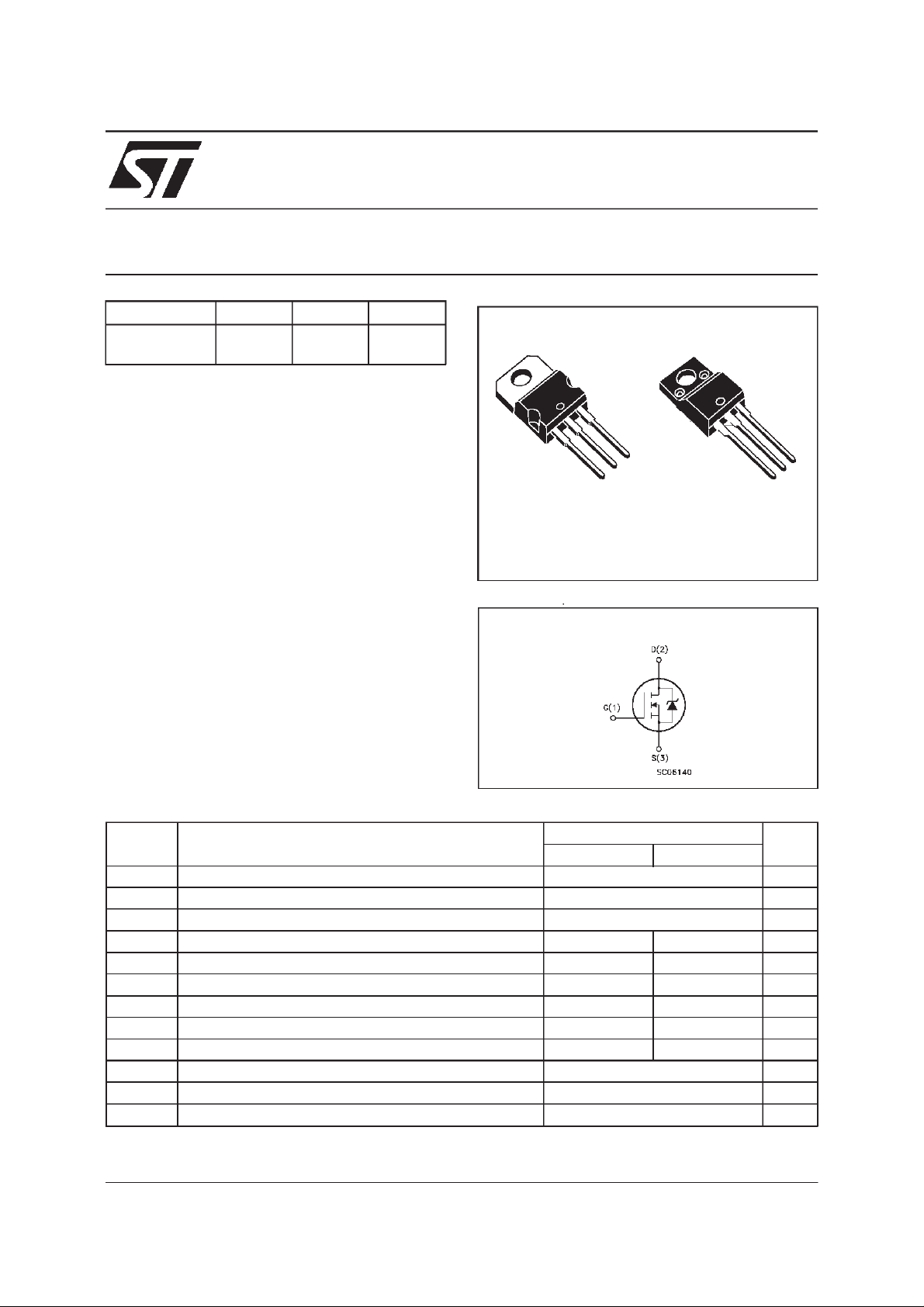
1
TO-220 TO-220FP
INTERNAL SCHEMATIC DIAGRAM
3
2
1
APPLICATIONS
■ DC MOTOR CONTROL
■ DC-DC& DC-AC CONVERTERS
■ SYNCHRONOUSRECTIFICATION
ABSOLUTE MAXIMUM RATINGS
Symbol Parameter Value Unit
ST P30NE06 STP30 NE 0 6F P
V
V
V
I
DM
P
V
dV/d t Peak Diode Recov er y voltage sl ope 7 V/ns
T
(•) Pulse width limited by safeoperating area (1)I
’
January 1999
Dra in- sour c e V ol t age (VGS=0) 60 V
DS
Dra in- gate Voltage (RGS=20kΩ)
DGR
Gat e-source Volt age ± 20 V
GS
Dra in Curr ent (continuous) at Tc=25oC3017A
I
D
Dra in Curr ent (continuous) at Tc=100oC2112A
I
D
60 V
(•) Dra in Curr ent (pulsed) 120 68 A
Tot al Dis s ipation at Tc=25oC8030W
tot
Der ati ng F actor 0.53 0.2 W/
Insulation Withstand Voltage (DC) 2000 V
ISO
St orage Temperature -65 to 175
stg
Max. Oper at ing Junc t ion Temperature 175
T
j
≤
30 A, di/dt≤300A/µs, V
SD
DD
≤
V
(BR)DSS,Tj
≤
T
JMAX
o
C
o
C
o
C
1/6
Page 2
STP30NE06/FP
THERMAL DATA
TO-220 TO-220FP
R
thj-case
R
thj-amb
R
thc-sink
T
AVALANCHE CHARACTERISTICS
Symbol Parameter Max Value U ni t
I
AR
E
Ther mal Resistanc e Junct ion-case Max 1.87 5
Ther mal Resistanc e Junct ion-ambient Max
Ther mal Resistanc e Case-sink Ty p
Maximum Lead Temperat ure F or Soldering Purpos e
l
Avalanche Current, Repetitive or Not-Repetitive
(pulse width limited by T
Single Puls e Avalanche E nergy
AS
(starting T
=25oC, ID=IAR,VDD=30V)
j
max)
j
62.5
0.5
300
30 A
100 mJ
o
C/W
o
C/W
o
C/W
o
C
ELECTRICAL CHARACTERISTICS
=25oC unless otherwisespecified)
(T
case
OFF
Symbol Parameter Test Con ditions Min. Typ. Max. Unit
V
(BR)DSS
Drain-source
=250µAVGS=0
I
D
60 V
Break dow n Vo lt age
I
DSS
I
GSS
Zero Gate Voltage
Drain Curre nt (V
GS
Gat e- bod y Leakag e
Current (V
DS
=0)
=0)
V
=MaxRating
DS
=MaxRating Tc=125oC
V
DS
=± 20 V
V
GS
1
10
± 100 nA
ON (∗)
Symbol Parameter Test Con ditions Min. Typ. Max. Unit
V
GS(th)
R
DS(on)
Gate Threshold Voltage
Sta t ic Drain-source On
V
DS=VGSID
= 250µA
VGS=10V ID= 15 A 0.042 0.050 Ω
234V
Resistance
I
D(on)
On State Drain Current VDS>I
D(on)xRDS(on )max
30 A
VGS=10V
DYNAMIC
Symbol Parameter Test Con ditions Min. Typ. Max. Unit
g
(∗)Forward
fs
Tr ansc on duc tance
C
C
C
Input Capacit anc e
iss
Out put Capacit ance
oss
Reverse Transfer
rss
Capacit a nc e
VDS>I
D(on)xRDS(on )maxID
=15 A 7 13 S
VDS=25V f=1MHz VGS= 0 1450
200
45
µ
µA
pF
pF
pF
A
2/6
Page 3

STP30NE06/FP
ELECTRICAL CHARACTERISTICS
(continued)
SWITCHING ON
Symbol Parameter Test Con ditions Min. Typ. Max. Unit
t
d(on)
Q
Q
Q
Turn-on Time
t
Rise Time
r
Tot al Gate C har ge
g
Gat e- Source Charge
gs
Gate-Drain Charge
gd
VDD=30V ID=15A
R
G
=4.7
Ω
V
GS
=10V
VDD=48V ID=30A VGS=10V 35
18
95
50 nC
10
13
SWITCHING OFF
Symbol Parameter Test Con ditions Min. Typ. Max. Unit
t
r(Voff)
t
t
Off-volt age Rise Time
Fall T ime
f
Cross-over Time
c
VDD=48V ID=30A
=4.7 ΩVGS=10V
R
G
10
41
60
SOURCEDRAINDIODE
Symbol Parameter Test Con ditions Min. Typ. Max. Unit
I
SD
I
SDM
V
SD
t
Q
I
RRM
(∗) Pulsed: Pulse duration = 300 µs, duty cycle 1.5 %
(•) Pulse width limited by safe operating area
Source-drain Current
(•)
Source-drain Current
30
120
(pulsed)
(∗)ForwardOnVoltage ISD=30A VGS=0 1.5 V
Reverse Recovery
rr
Time
Reverse Recovery
rr
= 30 A di/dt = 100 A/µs
I
SD
=30V Tj= 150oC
V
DD
85
0.19
Charge
Reverse Recovery
4.5
Current
ns
ns
nC
nC
ns
ns
ns
A
A
ns
µ
A
C
3/6
Page 4

STP30NE06/FP
TO-220 MECHANICAL DATA
DIM.
MIN. TYP. MAX. MIN. TYP. MAX.
A 4.40 4.60 0.173 0.181
C 1.23 1.32 0.048 0.051
D 2.40 2.72 0.094 0.107
D1 1.27 0.050
E 0.49 0.70 0.019 0.027
F 0.61 0.88 0.024 0.034
F1 1.14 1.70 0.044 0.067
F2 1.14 1.70 0.044 0.067
G 4.95 5.15 0.194 0.203
G1 2.4 2.7 0.094 0.106
H2 10.0 10.40 0.393 0.409
L2 16.4 0.645
L4 13.0 14.0 0.511 0.551
L5 2.65 2.95 0.104 0.116
L6 15.25 15.75 0.600 0.620
L7 6.2 6.6 0.244 0.260
L9 3.5 3.93 0.137 0.154
DIA. 3.75 3.85 0.147 0.151
mm inch
E
A
L4
D
F2
F1
G1
H2
G
F
P011C
C
D1
L2
Dia.
L5
L7
L6
L9
4/6
Page 5

TO-220FP MECHANICAL DATA
STP30NE06/FP
DIM.
MIN. TYP. MAX. MIN. TYP. MAX.
A 4.4 4.6 0.173 0.181
B 2.5 2.7 0.098 0.106
D 2.5 2.75 0.098 0.108
E 0.45 0.7 0.017 0.027
F 0.75 1 0.030 0.039
F1 1.15 1.7 0.045 0.067
F2 1.15 1.7 0.045 0.067
G 4.95 5.2 0.195 0.204
G1 2.4 2.7 0.094 0.106
H 10 10.4 0.393 0.409
L2 16 0.630
L3 28.6 30.6 1.126 1.204
L4 9.8 10.6 0.385 0.417
L6 15.9 16.4 0.626 0.645
L7 9 9.3 0.354 0.366
Ø 3 3.2 0.118 0.126
mm inch
E
A
D
B
L3
L6
L7
¯
F1
F
G1
H
G
F2
123
L2
L4
5/6
Page 6

STP30NE06/FP
Information furnished is believed to be accurate and reliable. However, STMicroelectronics assumes no responsibility forthe consequences
of use of such information nor for any infringement of patents or other rights of third parties which may result from its use. No license is
granted by implicationor otherwise under any patent or patent rights of STMicroelectronics. Specification mentioned in this publication are
subject to change without notice. This publication supersedes and replaces all information previously supplied. STMicroelectronics products
are not authorized for use as critical components inlife support devices or systems without express written approval of STMicroelectronics.
The ST logo is a trademarkof STMicroelectronics
1998 STMicroelectronics – Printed in Italy – All Rights Reserved
STMicroelectronics GROUP OF COMPANIES
Australia - Brazil - Canada -China -France - Germany - Italy - Japan - Korea -Malaysia - Malta - Mexico - Morocco - The Netherlands -
Singapore - Spain - Sweden - Switzerland - Taiwan - Thailand - United Kingdom - U.S.A.
http://www.st.com
.
6/6
 Loading...