

Page 1
STP3020L
N - CHANNEL 30V - 0.019Ω - 40A - TO-220
STripFET POWER MOSFET
TYPE V
DSS
R
DS(on)
I
D
ST P3020L 30 V < 0.022 Ω 40 A
■ TYPICALR
■ LOW GATE CHARGE A 100
■ APPLICATIONORIENTED
DS(on)
= 0.019 Ω
o
C
CHARACTERIZATION
DESCRIPTION
This Power Mosfet is the latest development of
STMicroelectronics unique ”Single Feature
Size” strip-based process. The resulting transi-
stor showsextremelyhigh packingdensity forlow
on-resistance, rugged avalance characteristics
and less critical alignment steps therefore a remarkablemanufacturingreproducibility.
APPLICATIONS
■ HIGHCURRENT, HIGH SPEEDSWITCHING
SOLENOIDANDRELAY DRIVERS
■ MOTORCONTROL, AUDIOAMPLIFIERS
■ DC-AC & DC-AC CONVERTERS IN HIGH
PERFORMANCE VRMs
■ AUTOMOTIVE ENVIRONMENT (INJECTION,
ABS, AIR-BAG, LAMPDRIVERS,Etc.)
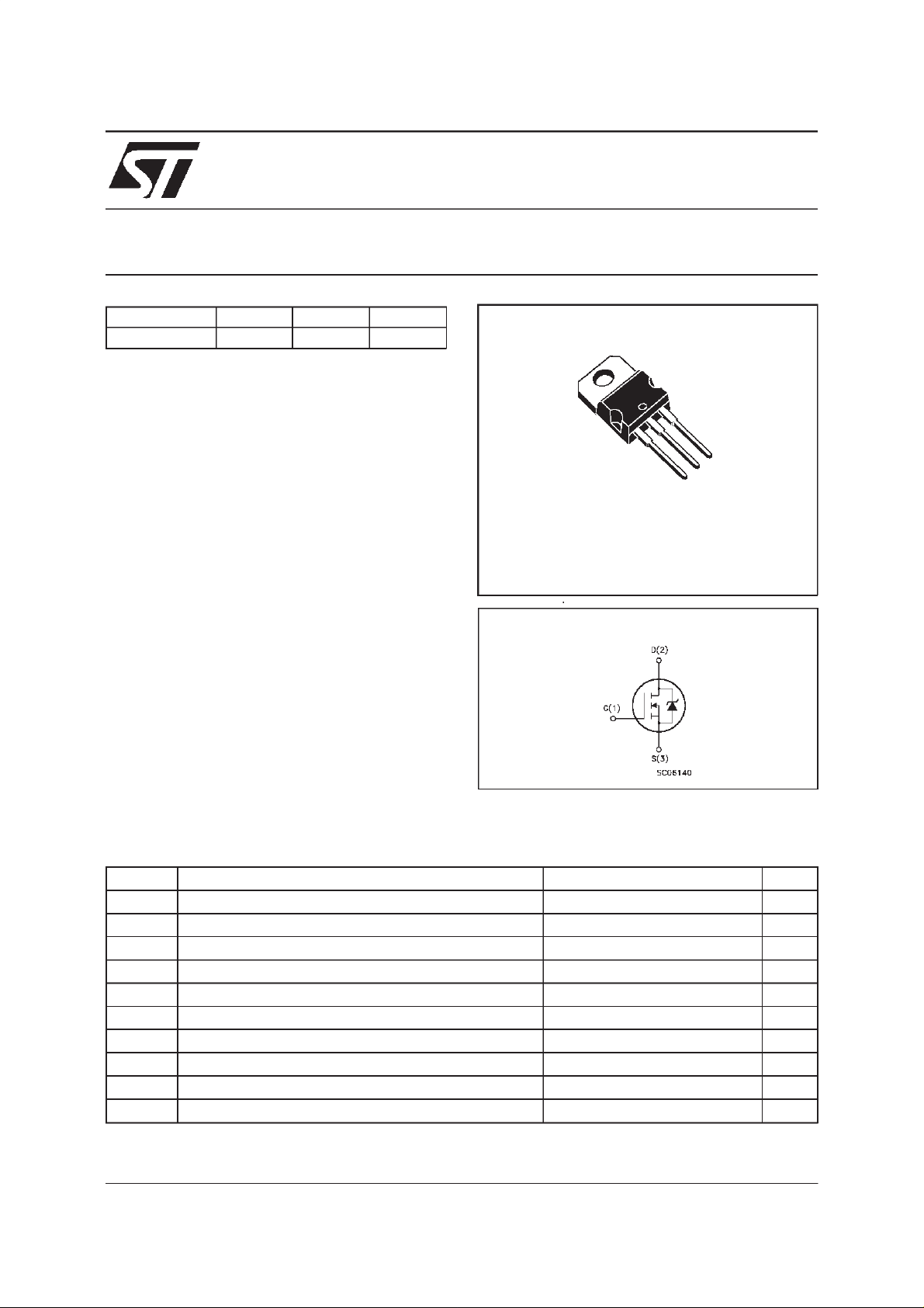
3
2
1
TO-220
INTERNAL SCHEMATIC DIAGRAM
ABSOLUTE MAXIMUM RATINGS
Symb o l Parameter Val u e Uni t
V
V
V
I
DM
P
T
(•) Pulse width limited by safe operating area
March 1999
Drain-sourc e V o lt age (VGS=0) 30 V
DS
Drain- ga t e Voltage (RGS=20kΩ)30V
DGR
Gate-s ource Volt age
GS
I
Drain Cur rent (c ont i nuous) at Tc=25oC40A
D
I
Drain Cur rent (c ont i nuous) at Tc= 100oC28A
D
20 V
±
(•) Drain Current (pulsed) 160 A
Total Dissipation at Tc=25oC80W
tot
Derating Factor 0.53 W/
St orage T em p erat ure -65 to 175
stg
T
Max. Operating Junct ion Tem p er at u re 175
j
o
C
o
C
o
C
1/8
Page 2
STP3020L
THERMAL DATA
R
thj-case
Rthj-amb
R
thc-sink
T
Ther mal Resistanc e Junct ion-case Max
Ther mal Resistanc e Junct ion-ambient Max
Ther mal Resistanc e Case-sink Ty p
Maximum L ead Tem pe ra t ure For Soldering Purpose
l
1.875
62.5
0.5
300
o
C/W
oC/W
o
C/W
o
C
ELECTRICAL CHARACTERISTICS
=25oC unless otherwisespecified)
(T
case
OFF
Symbol Parameter Test Conditions Min. Typ. M ax. Unit
V
(BR)DSS
Drain-source
ID=250µAVGS=0 30 V
Break dow n Vo lt age
I
DSS
I
GSS
Zero Gate Voltage
Drain Curre nt (V
GS
Gat e- bod y Leakage
Current (V
DS
=0)
=0)
V
=MaxRating
DS
=MaxRating Tc=125oC
V
DS
V
= ± 20 V ± 100 nA
GS
1
10
ON (∗)
Symbol Parameter Test Conditions Min. Typ. M ax. Unit
V
GS(th)
R
DS(on)
I
D(on)
Gate Threshold Voltage VDS=VGSID= 250 µ A12.5V
Sta t ic Drain-s ource On
Resistance
VGS=10V ID=20A
=5V ID=20A
V
GS
On State Drain Current VDS>I
D(on)xRDS(on)max
0.019
0.033
40 A
0.022
0.038ΩΩ
VGS=10V
DYNAMIC
Symbol Parameter Test Conditions Min. Typ. M ax. Unit
g
(∗)Forward
fs
Tr ansc on duc tance
C
C
C
Input Capaci t ance
iss
Out put Capac it anc e
oss
Reverse Transfer
rss
Capacit a nc e
VDS>I
D(on)xRDS(on)maxID
=20 A 5 20 S
VDS=25V f=1MHz VGS= 0 1270
350
115
µ
µA
pF
pF
pF
A
2/8
Page 3
STP3020L
ELECTRICAL CHARACTERISTICS
(continued)
SWITCHING ON
Symbol Parameter Test Conditions Min. Typ. M ax. Unit
t
d(on)
Tur n-on Delay Time
Rise Time
t
r
VDD=15V ID=19A
R
=4.7
G
Ω
VGS=4.5V
28
220
(Resis t iv e Load, see fig. 3)
Q
Q
Q
Tot al Gate Char ge
g
Gat e- Source Charge
gs
Gate-Drain Charge
gd
VDD=24V ID=38A VGS=5V 21
9
11
29 nC
SWITCHING OFF
Symbol Parameter Test Conditions Min. Typ. M ax. Unit
t
d(off)
Tur n-of f Dela y Tim e
t
Fall T ime
f
VDD=15V ID=19A
=4.7 Ω VGS=4.5V
R
G
45
35
(Resis t iv e Load, see fig. 3)
t
r(Voff)
t
t
Off-voltage Rise Time
Fall T ime
f
Cross-over Tim e
c
VDD=24V ID=38A
=4.7 Ω VGS=4.5V
R
G
(Indu ct iv e Load, see fig. 5)
30
85
125
SOURCEDRAINDIODE
Symbol Parameter Test Conditions Min. Typ. M ax. Unit
I
SDM
V
I
SD
Q
I
RRM
SD
t
Source-drain Current
(•)
Source-drain Current
40
160
(pulsed)
(∗)ForwardOnVoltage ISD=40A VGS=0 1.5 V
Reverse Recovery
rr
Time
Reverse Recovery
rr
ISD= 38 A di/dt = 100 A/µs
=15V Tj=150oC
V
DD
(see test circuit, fig. 5)
45
60
Charge
Reverse Recovery
2.5
Current
ns
ns
nC
nC
ns
ns
ns
ns
ns
A
A
ns
nC
A
(∗) Pulsed:Pulse duration= 300µs, duty cycle 1.5%
(•) Pulse width limited by safeoperating area
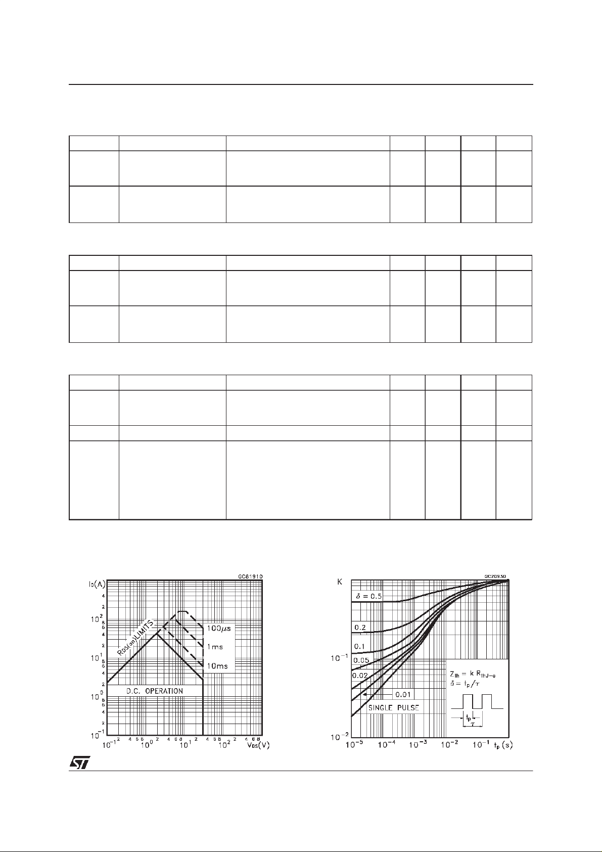
SafeOperating Area ThermalImpedance
3/8
Page 4

STP3020L
OutputCharacteristics
Transconductance
TransferCharacteristics
Static Drain-sourceOn Resistance
Gate Charge vs Gate-sourceVoltage
4/8
CapacitanceVariations
Page 5

STP3020L
NormalizedGate ThresholdVoltage vs
Temperature
Source-drainDiode Forward Characteristics
NormalizedOn Resistancevs Temperature
5/8
Page 6

STP3020L
Fig. 1: UnclampedInductiveLoad Test Circuit
Fig. 3: SwitchingTimesTest CircuitsFor
ResistiveLoad
Fig. 2:UnclampedInductive Waveform
Fig. 4: Gate Charge test Circuit
Fig. 5: TestCircuit ForInductiveLoad Switching
And Diode Recovery Times
6/8
Page 7

TO-220 MECHANICALDATA
STP3020L
DIM.
MIN. TYP. MAX. MIN. TYP. MAX.
A 4.40 4.60 0.173 0.181
C 1.23 1.32 0.048 0.051
D 2.40 2.72 0.094 0.107
D1 1.27 0.050
E 0.49 0.70 0.019 0.027
F 0.61 0.88 0.024 0.034
F1 1.14 1.70 0.044 0.067
F2 1.14 1.70 0.044 0.067
G 4.95 5.15 0.194 0.203
G1 2.4 2.7 0.094 0.106
H2 10.0 10.40 0.393 0.409
L2 16.4 0.645
L4 13.0 14.0 0.511 0.551
L5 2.65 2.95 0.104 0.116
L6 15.25 15.75 0.600 0.620
L7 6.2 6.6 0.244 0.260
L9 3.5 3.93 0.137 0.154
DIA. 3.75 3.85 0.147 0.151
mm inch
E
A
L4
D
F2
F1
G1
H2
G
F
P011C
C
D1
L2
Dia.
L5
L7
L6
L9
7/8
Page 8

STP3020L
Information furnished is believed tobeaccurate and reliable. However, STMicroelectronics assumes no responsibilityforthe consequences
of use of such information nor for any infringement of patents or other rights of third parties which may result from its use. No licenseis
granted by implication orotherwise under any patent or patentrights of STMicroelectronics. Specificationmentioned in this publicationare
subjectto change without notice.Thispublication supersedes and replacesall information previouslysupplied. STMicroelectronics products
are not authorizedfor use as critical components in life support devices or systemswithout express written approval of STMicroelectronics.
The STlogo is a trademark ofSTMicroelectronics
1999 STMicroelectronics – Printed in Italy – All Rights Reserved
STMicroelectronics GROUP OF COMPANIES
Australia - Brazil - Canada - China -France - Germany - Italy - Japan- Korea - Malaysia - Malta - Mexico- Morocco - The Netherlands -
8/8
Singapore - Spain - Sweden - Switzerland - Taiwan- Thailand - United Kingdom - U.S.A.
http://www.st.com
.
 Loading...