

Page 1
STP2N60
STP2N60FI
N - CHANNEL ENHANCEMENT MODE
POWER MOS TRANSISTOR
TYPE V
STP 2N60
STP 2N60FI
■ TYPICAL R
■ AVALANCHE RUGGED TECHNOLOGY
■ 100% AVALANCHE TESTED
■ REPETITIVE AVALANCHE DATA AT 100
■ APPLICATION ORIENTED
DS(on)
DSS
600 V
600 V
= 3.2 Ω
R
DS(on)
<3.5Ω
<3.5Ω
I
D
2.9 A
2.2 A
o
C
CHARACTERIZATION
APPLICATIONS
■ HIGH CURRENT, HIGH SPEED SWITCHING
■ SWITCH MODE POWERSUPPLIES (SMPS)
■ CHOPPER REGULATORS, CONVERTERS,
MOTOR CONTROL, LIGHTING FOR
INDUSTRIAL AND CONSUMER
ENVIRONMENT
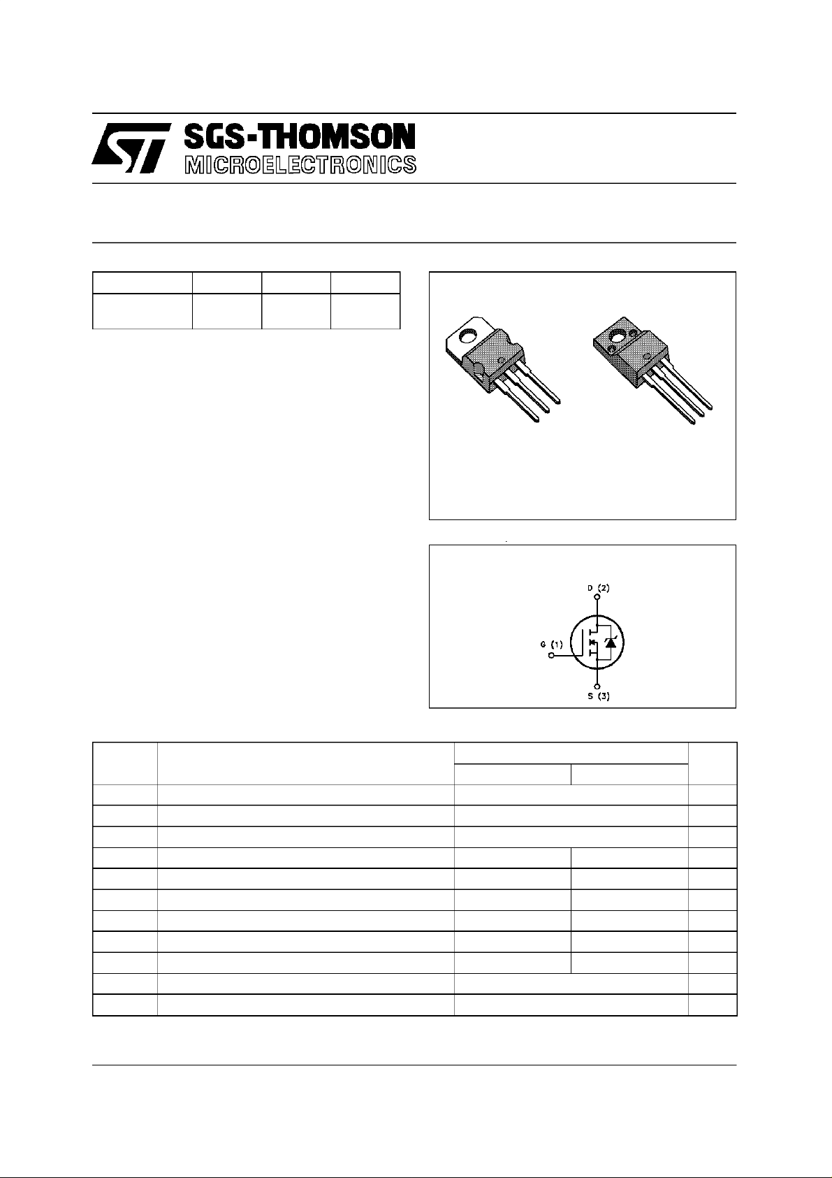
3
2
1
TO-220 ISOWATT220
INTERNAL SCHEMATIC DIAGRAM
3
2
1
ABSOLUTE MAXIMUM RATINGS
Symb o l Paramet er Val u e Unit
STP2N60 STP2N60FI
V
V
V
I
DM
P
V
T
(•) Pulsewidth limited bysafe operating area
December 1996
Drain - s ource Voltage (VGS=0) 600 V
DS
Drain- gate Voltage (RGS=20kΩ)600V
DGR
Gate-source Voltage ± 20 V
GS
Drain Current (continuous) at Tc=25oC2.92.2A
I
D
Drain Current (continuous) at Tc=100oC1.7 1.3A
I
D
(•) Drain Current (pulsed) 11 11 A
Total Di ssipation a t Tc=25oC7035W
tot
Derat ing Factor 0.56 0.28 W/
Ins ulation Withs t and Voltage (DC) 2000 V
ISO
St or a ge Tem perature -65 t o 150
stg
Max. Operating Jun ction T emperature 150
T
j
o
o
o
C
C
C
1/10
Page 2

STP2N60/FI
THERMAL DATA
TO-220 ISOW ATT 220
R
thj-case
R
thj-amb
R
thc-sink
T
AVALANCHE CHARACTERISTICS
Symbol Parameter Max Value Uni t
I
AR
E
E
I
AR
Thermal Resistance Junction - cas e M ax 1.78 3.57
Thermal Resistance Junction- ambient Max
Thermal Resistance Case-sink Typ
Maximum Lead Temperature For So ldering Purpose
l
Avalanc h e Cu rr ent , Repet itive or Not-Rep etitive
(pulse width limited by Tjmax, δ <1%)
Single Pul se Avalanche Ener gy
AS
(starti ng T
Repetitive Avalanc he Energ y
AR
=25oC, ID=IAR,VDD=50V)
j
(pulse width limited by Tjmax, δ <1%)
Avalanc h e Cu rr ent , Repet itive or Not-Rep etitive
(Tc= 100oC, pulse width l imited by Tjmax, δ <1%)
62.5
0.5
300
2.9 A
105 mJ
3.5 mJ
1.7 A
o
C/W
o
C/W
o
C/W
o
C
ELECTRICAL CHARACTERISTICS (T
=25oC unless otherwisespecified)
case
OFF
Symbol Parameter Test Co ndi tions Min. Typ. Max. Unit
V
(BR)DSS
Drain - s ource
ID=250µAVGS= 0 600 V
Break d own Volta ge
I
DSS
I
GSS
Zer o G at e V oltage
Drain Current (VGS=0)
Gat e- body Leakage
Current (V
DS
=0)
VDS=MaxRating
VDS= Max Rating x 0.8 Tc=125oC
= ± 20 V ± 10 0 nA
V
GS
25
250
ON (∗)
Symbol Parameter Test Co ndi tions Min. Typ. Max. Unit
V
GS(th)
R
DS(on)
Gate Threshold Voltage VDS=VGSID=250µA234V
St at ic Drain-s our ce O n
VGS=10V ID= 1.5 A 3.2 3.5 Ω
Resistance
I
D(on)
On State Drain Current VDS>I
D(on)xRDS(on)max
2.9 A
VGS=10V
DYNAMIC
Symbol Parameter Test Co ndi tions Min. Typ. Max. Unit
(∗)Forward
g
fs
Tr ansconductance
C
C
C
Input Capacitance
iss
Out put Capacitance
oss
Reverse Transfer
rss
Capacitance
VDS>I
D(on)xRDS(on)maxID
=1.5A 1 2.4 S
VDS=25V f=1MHz VGS=0 450
62
23
600
85
35
µA
µA
pF
pF
pF
2/10
Page 3
STP2N60/FI
ELECTRICAL CHARACTERISTICS (continued)
SWITCHING ON
Symbol Parameter Test Co ndi tions Min. Typ. Max. Unit
t
d(on)
(di/dt)
Q
Q
Q
Turn-on T ime
t
Rise Time
r
Turn-on Current S lope VDD=480V ID=2.9A
on
Total Gate Charge
g
Gat e- Source Charge
gs
Gate-Drain Charge
gd
SWITCHING OFF
Symbol Parameter Test Co ndi tions Min. Typ. Max. Unit
t
r(Voff)
t
Off -voltage Rise Time
t
Fall Time
f
Cross-over Time
c
SOURCE DRAINDIODE
VDD=35V ID=2A
RG=50 Ω VGS=10V
25
11040150
(see test circuit, figure 3)
75 A/ µ s
RG=50 Ω VGS=10V
(see test circuit, figure 5)
VDD= 480 V ID=2.9A VGS=10V 33
7
13
VDD=480V ID=2.9A
RG=50 Ω VGS=10V
(see test circuit, figure 5)
70
20
100
45 nC
95
30
130
ns
ns
nC
nC
ns
ns
ns
Symbol Parameter Test Co ndi tions Min. Typ. Max. Unit
I
I
SDM
SD
Source-drain C urrent
(•)
Source-drain C urrent
2.9
11
(pulsed)
V
(∗) Forward On Voltage ISD=2.9A VGS=0 2 V
SD
t
Reverse Recovery
rr
Time
Q
Reverse Recovery
rr
ISD=2.9A di/dt=100A/µs
VDD=80V Tj=150oC
(see test circuit, figure 5)
500
7
Charge
I
RRM
Reverse Recovery
28
Current
(∗) Pulsed:Pulse duration = 300 µs, dutycycle 1.5 %
(•) Pulse widthlimited by safeoperating area
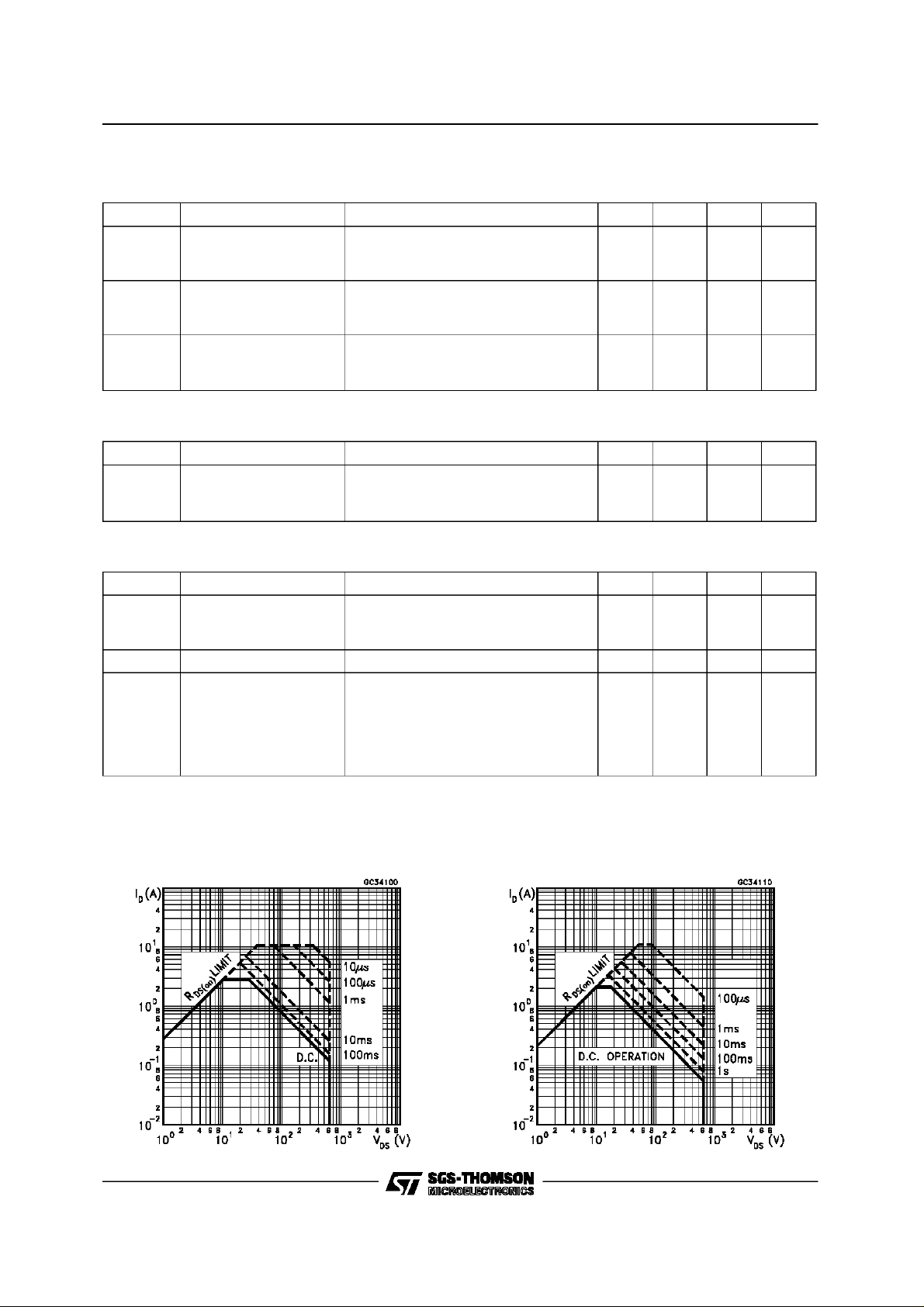
Safe Operating Areas For TO-220 Safe Operating Areas For ISOWATT220
A
A
ns
µC
A
3/10
Page 4

STP2N60/FI
Thermal ImpedeanceFor TO-220
Derating Curve For TO-220
Thermal ImpedanceFor ISOWATT220
Derating Curve For ISOWATT220
Output Characteristics
4/10
Transfer Characteristics
Page 5

Transconductance Static Drain-source On Resistance
Gate Charge vs Gate-source Voltage Capacitance Variations
STP2N60/FI
Temperature
Normalized On Resistance vs TemperatureNormalized Gate Threshold Voltage vs
5/10
Page 6

STP2N60/FI
Turn-on Current Slope Turn-off Drain-source Voltage Slope
Cross-over Time Switching Safe Operating Area
Accidental Overload Area Source-drain Diode ForwardCharacteristics
6/10
Page 7

STP2N60/FI
Fig. 1: Unclamped Inductive Load Test Circuits
Fig. 3: Switching Times Test Circuits For
Resistive Load
Fig. 2: Unclamped Inductive Waveforms
Fig. 4: Gate Charge Test Circuit
Fig. 5: Test Circuit For Inductive Load Switching
And Diode Reverse Recovery Time
7/10
Page 8

STP2N60/FI
TO-220 MECHANICAL DATA
DIM.
mm inch
MIN. TYP. MAX. MIN. TYP. MAX.
A 4.40 4.60 0.173 0.181
C 1.23 1.32 0.048 0.051
D 2.40 2.72 0.094 0.107
D1 1.27 0.050
E 0.49 0.70 0.019 0.027
F 0.61 0.88 0.024 0.034
F1 1.14 1.70 0.044 0.067
F2 1.14 1.70 0.044 0.067
G 4.95 5.15 0.194 0.203
G1 2.4 2.7 0.094 0.106
H2 10.0 10.40 0.393 0.409
L2 16.4 0.645
L4 13.0 14.0 0.511 0.551
L5 2.65 2.95 0.104 0.116
L6 15.25 15.75 0.600 0.620
L7 6.2 6.6 0.244 0.260
L9 3.5 3.93 0.137 0.154
DIA. 3.75 3.85 0.147 0.151
E
A
L4
D
F2
F1
G1
H2
G
F
C
D1
L2
Dia.
L5
L7
L6
L9
P011C
8/10
Page 9

ISOWATT220 MECHANICAL DATA
STP2N60/FI
DIM.
MIN. TYP. MAX. MIN. TYP. MAX.
A 4.4 4.6 0.173 0.181
B 2.5 2.7 0.098 0.106
D 2.5 2.75 0.098 0.108
E 0.4 0.7 0.015 0.027
F 0.75 1 0.030 0.039
F1 1.15 1.7 0.045 0.067
F2 1.15 1.7 0.045 0.067
G 4.95 5.2 0.195 0.204
G1 2.4 2.7 0.094 0.106
H 10 10.4 0.393 0.409
L2 16 0.630
L3 28.6 30.6 1.126 1.204
L4 9.8 10.6 0.385 0.417
L6 15.9 16.4 0.626 0.645
L7 9 9.3 0.354 0.366
Ø 3 3.2 0.118 0.126
mm inch
E
A
D
B
L3
L6
L7
Ø
F1
F
G1
H
G
F2
123
L2
L4
P011G
9/10
Page 10

STP2N60/FI
Information furnished is believed to be accurate and reliable. However, SGS-THOMSONMicroelectronics assumes no responsability for the
consequences of use of such information nor for any infringement of patents or otherrights of third parties which may results from its use.No
licenseis granted by implication or otherwise under any patentor patent rights of SGS-THOMSON Microelectronics. Specifications mentioned
in thispublication are subject to change withoutnotice. Thispublication supersedes andreplacesall information previously supplied.
SGS-THOMSONMicroelectronics products are not authorized for use ascritical components in lifesupport devices orsystemswithout express
writtenapproval ofSGS-THOMSONMicroelectonics.
1996 SGS-THOMSON Microelectronics -Printed in Italy- AllRightsReserved
Australia- Brazil - Canada -China - France- Germany - HongKong- Italy -Japan- Korea-Malaysia - Malta- Morocco- TheNetherlands -
Singapore - Spain - Sweden-Switzerland- Taiwan - Thailand- UnitedKingdom -U.S.A
SGS-THOMSONMicroelectronics GROUPOF COMPANIES
.
10/10
 Loading...