

Page 1
查询STB20NM50供应商
STB20NM50 - STB20NM50-1
STP20NM50 - STP20NM50FP
N-CHANNEL 550V@Tj
- 0.20Ω - 20A - TO220/FP-D²PAK-I²PAK
max
Zener-Protected SuperMESH™ MOSFET
General features
V
Type
STB20NM50
STB20NM50-1
STP20NM50
STP20NM50FP
■ HIGH dv/dt A ND AVALANCHE CAPABILITIES
■ 100% AVALANCHE TESTED
■ LOW INPUT CAPACITANCE AND GATE
DSS(@Tj
max)
550 V
550 V
550 V
550 V
CHARGE
■ LOW GATE INPUT RESISTANCE
Description
R
DS(on)
<0.25 Ω
<0.25 Ω
<0.25 Ω
<0.25 Ω
I
D
20 A
20 A
20 A
20 A
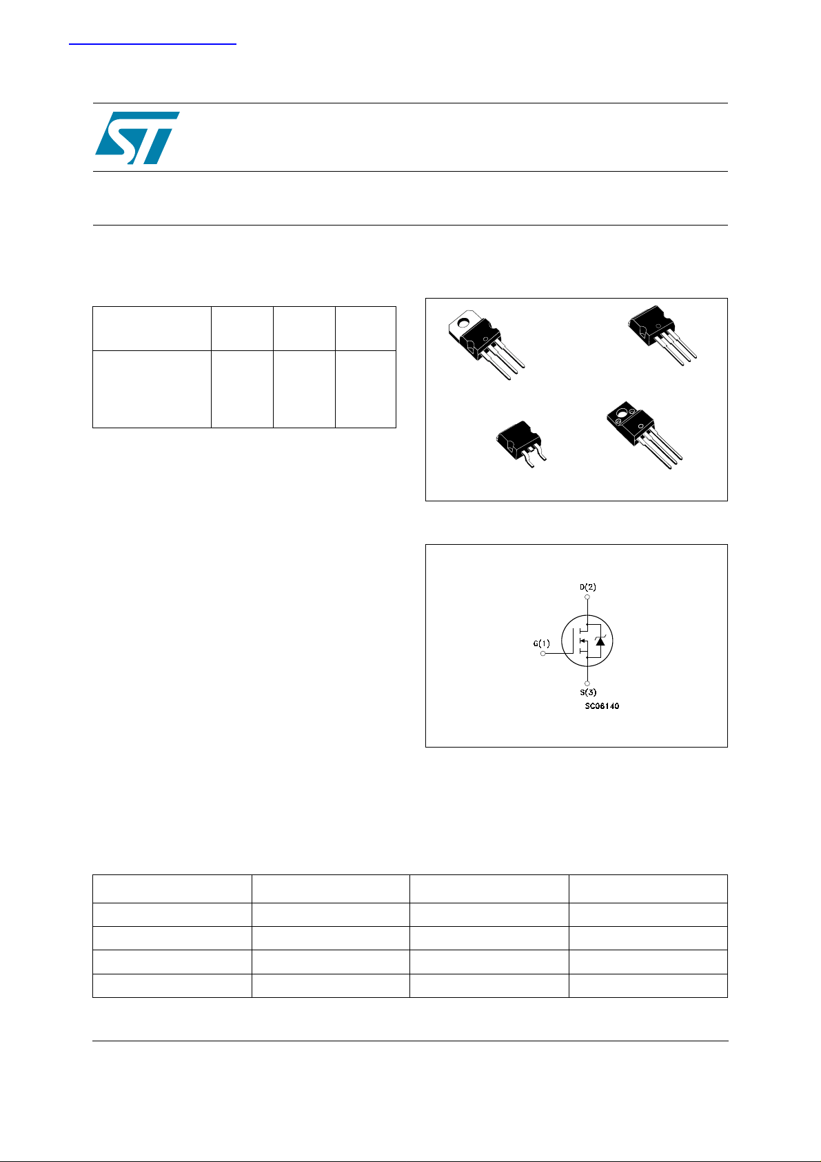
Package
3
2
TO-220
1
D²PAK
3
1
I²PAK
1
TO-220FP
Internal schematic diagram
3
2
1
3
2
The MDmesh™ is a new revolutionary MOSFET
technology that associates the Multiple Drain
process with the Company’s
PowerMESH™horizontal layout. The resulting
product has an outstanding low on-resistance,
impressively high dv/dt and exellent avalanche
characteristics and dynamic performances.
Applications
The MDmesh™ family is very suitable for
increasing power density of high voltage
converters allowing system miniaturization
andhiher efficiencies
Order codes
Sales Type Marking Package Packaging
STB20NM50T4 B20NM50 D²PAK TAPE & REEL
STB20NM50-1 B20NM50-1 I²PAK TUBE
STP20NM505 P20NM50 TO-220 TUBE
STP20NM50FP P20NM50FP TO-220FP TUBE
Rev 2
September 2005 1/16
www.st.com
16
Page 2
1 Electrical ratings STB20NM50-1 - STB20N M50 - STP2 0N M50 - STP20NM50F P
1 Electrical ratings
Table 1. Absolute maximum ratings
Symbol Parameter Value Unit
TO-220/D²PAK/I²PAK TO-220FP
I
DM
V
GS
I
D
I
D
Note 2
P
TOT
Gate-Source Voltage ± 30 V
Drain Current (continuous) at TC = 25°C
Drain Current (continuous) at TC = 100°C
20 20 (Note3) A
12.6 12.6 (Note 3) A
Drain Current (pulsed) 80 80 (Note3) A
Total Dissipation at TC = 25°C
192 45 W
Derating Factor 1.2 0.36 W/°C
dv/dt Note 1 Peak Diode Recovery voltage slope 15 V/ns
V
ISO
T
T
stg
Insulation Withstand Volatge (DC) -- 2000 V
Operating Junction Temperature
j
Storage Temperature
-65 to 150 °C
Table 2. Thermal data
TO-220/D²PAK/I²PAK TO-220FP Unit
Rthj-case Thermal Resistance Junction-case Max 0.65 2.8 °C/W
Rthj-amb Thermal Resist ance Junction-amb Max 62.5 °C/W
T
l
Maximum Lead Temperature For Solder ing
Purpose
300 °C
Table 3. Avalanche characteristics
Symbol Parameter Max Valu e Unit
I
AR
E
AS
2/16
Avalanche Curren t, repetitive or
Not-Repetitive (pul se width limited by Tj max)
Single Pulse Avalanche Energy
(starting Tj=25°C, I
=5A, VDD= 50V)
D
10 A
650 mJ
Page 3
STB20NM 50-1 - STB20NM50 - ST P20NM50 - STP20NM 50FP 2 Electrical characteristics
2 Electrical characteristics
(T
= 25 °C unless otherwise specified)
CASE
Table 4. On/off states
Symbol Parameter Test Conditions Min. Typ. Max. Unit
V
(BR)DSS
I
DSS
I
GSS
V
GS(th)
R
DS(on)
Drain-Source Breakdown
Voltage
Zero Gate Voltage Drain
Current (V
GS
= 0)
Gate Body Leakage Current
= 0)
(V
DS
Gate Threshold Voltage
St ati c Drai n-Source On
Resistance
I
= 250µA, VGS= 0
D
= Max Ra ting,
V
DS
V
= Max Rating,Tc = 125°C
DS
= ±30V
V
GS
= VGS, ID = 250 µA
V
DS
V
= 10 V, ID= 10 A
GS
500 V
1
10
±100 µA
345V
0.20 0.25 Ω
Table 5. Dynamic
Symbol Parameter Test Conditions Min. Typ. Max. Unit
> I
V
DS
Note 4
g
fs
C
C
C
C
oss eq.
Note 5
iss
oss
rss
Forward Transconductance
Input Capaci tance
Outp u t C a pacita nce
Rev er se Trans fer Ca pa citan ce
Equivalent Ouput Capacitance
D(ON) xRDS(ON)max,
ID = 10A
=25V, f=1 MHz, VGS=0
V
DS
=0, V
V
GS
=0V to 400V
DS
10 S
1480
285
34
130 pF
µA
µA
pF
pF
pF
Rg Gate Input Resistance
Q
g
Q
gs
Q
gd
Total Gate Charge
Gate-Source Charge
Gate-Drain Charge
f=1MHz Gate DC Bias=0
Test Signal Level=20mV
Open Drain
=400V, ID = 20A
V
DD
=10V
V
GS
(see Figure 15)
1.6 Ω
40
13
19
56 nC
nC
nC
3/16
Page 4

2 Electric al characteristics STB20N M 50-1 - STB20NM50 - ST P20NM 50 - STP20NM 50FP
Table 6. Switching times
Symbol Parameter Test Conditions Min. Typ. Max. Unit
V
=250 V, ID=10A,
t
d(on)
Tur n-o n Delay Time
t
r
Rise Time
DD
=4.7Ω, VGS=10V
R
G
(see Figure 16)
24
16
ns
ns
t
r(Voff)
t
Off-vol tage Rise Time
t
f
c
Fall Ti me
Cross-over T ime
=400 V, ID=20A,
V
DD
=4.7Ω, VGS=10V
R
G
(see Figure 16)
9
8.5
23
Table 7. Source drain diode
Symbol Parameter Test Conditions Min. Typ. Max. Unit
I
SD
I
Note 2
SDM
V
Note 4
SD
t
rr
Q
rr
I
RRM
t
rr
Q
rr
I
RRM
(1) ISD ≤20A, di/dt ≤400A/µs, VDD ≤ V
(2) Pul s e width limited by safe op erating area
(3) Limited only by maximum temperature allowed
(4) Pulsed: pulse duration = 300µs, duty cycle 1.5%
(5) C
oss eq.
to 80% V
Source-drain Current
Source-drain Current (pulsed)
, Tj ≤ T
JMAX
ISD=20A, VGS=0
=20A, di/dt = 100A/µs,
I
SD
V
=100 V, Tj=25°C
DD
=20A, di/dt = 100A/µs,
I
SD
V
=100 V, Tj=150°C
DD
Forward on Voltage
Reverse Recovery Time
Reverse Recovery Charge
Reverse Recovery Current
Reverse Recovery Time
Reverse Recovery Charge
Reverse Recovery Current
(BR)DSS
is defined as a constant equivalent capacitance giving the same charging time as C
DSS
20
80
1.5 V
350
4.6
26
435
5.9
27
when VDS increases from 0
oss
ns
ns
ns
A
A
ns
µC
A
ns
µC
A
4/16
Page 5
STB20NM 50-1 - STB20NM50 - ST P20NM50 - STP20NM 50FP 2 Electrical characteristics
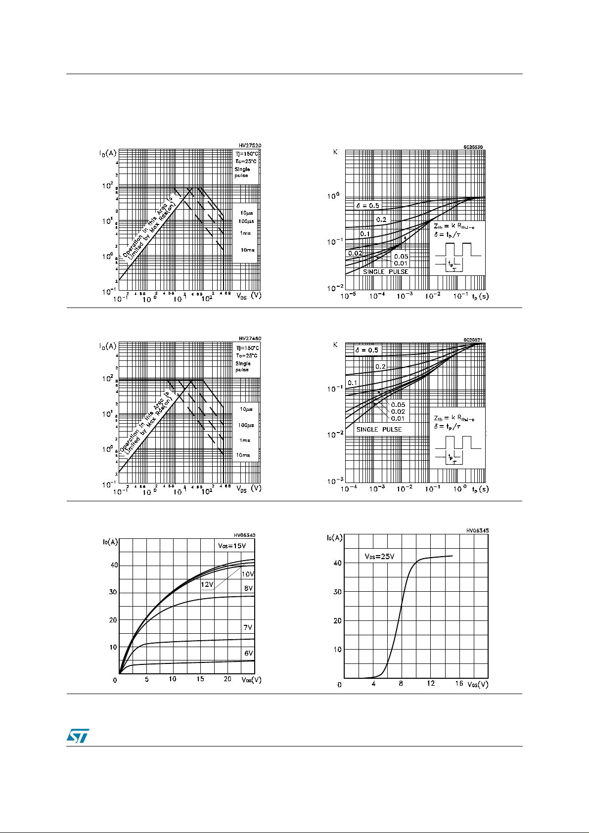
2.1 Electrical Characteristics (curves)
Figure 1. Safe Ope ra tin g A rea for
TO-220/D²PAK/I²PAK
Figure 3. Safe Operating Area for TO-220FP Figure 4. Th ermal Impedance for TO-220FP
Figure 2. Therm al Impedance for
TO-220/D²PAK/I²PAK
Figure 5. Output Characteristics Figure 6. Transfer Characteristics
5/16
Page 6

2 Electric al characteristics STB20N M 50-1 - STB20NM50 - ST P20NM 50 - STP20NM 50FP
Figure 7. Transconductance Figure 8. Static Drain-Source on Resistance
Figure 9. Gate Charge vs Gate -Source
Voltage
Figure 10. Normalized Gate Th reshold Voltage
vs Tem p eratu te
Figure 11. Capacitance Variations
Figure 12. Normalized on Resistance vs
Tem perature
6/16
Page 7

STB20NM 50-1 - STB20NM50 - ST P20NM50 - STP20NM 50FP 2 Electrical characteristics
Figure 13. Source-drain Diode Forward
Characteristics
7/16
Page 8

3 Test circuits STB20N M 50-1 - STB20NM50 - ST P20NM 50 - STP20NM 50FP
3 Test circuits
Figure 14. Switching Times Test Circuit For
Resistive Load
Figure 16. Test Circuit For Indictive Load
Switching and Diode Recovery
Times
Figure 15. Gate Charge Test Circuit
Figure 18. Unclamped Inductive Load Test
Circuit
Figure 17. Unclamped Inductive Waveform
8/16
Page 9

STB20NM 50-1 - STB20NM50 - ST P20NM50 - STP20NM 50FP 4 Package mechanical data
4 Package m echanical data
In order to meet environmental requirements, ST offers these devices in ECOPACK®
packages. These packages have a Lead-free second level interconnect . The category of
second level interconnect is marked on the package and on the inner box label, in compliance
with JEDEC Standard JESD97. The maximum ratings related to soldering conditions are also
marked on the inner box label. ECOPACK is an ST trademark. ECOPACK specifications are
available at: www.st.com
9/16
Page 10

4 Package mechani cal data STB 20NM50-1 - STB20N M 50 - STP20NM50 - ST P20NM50F P
TO-220 MECHANICAL DATA
DIM.
A 4.40 4.60 0.173 0.181
b 0.61 0.88 0.024 0.034
b1 1.15 1.70 0.045 0.066
c 0.49 0.70 0.019 0.027
D 15.25 15.75 0.60 0.620
E 10 10.40 0.393 0.409
e 2.40 2.70 0.094 0.106
e1 4.95 5.15 0.194 0.202
F 1.23 1.32 0.048 0.052
H1 6.20 6.60 0.244 0.256
J1 2.40 2.72 0.094 0.107
L 13 14 0.511 0.551
L1 3.50 3.93 0.137 0.154
L20 16.40 0.645
L30 28.90 1.137
øP 3.75 3.85 0.147 0.151
Q 2.65 2.95 0.104 0.116
MIN. TYP MAX. MIN. TYP. MAX.
mm. inch
10/16
Page 11

STB20NM 50-1 - STB20NM50 - ST P20NM50 - STP20NM 50FP 4 Package mechanical data
TO-220FP MECHANICAL DATA
DIM.
A 4.4 4.6 0.173 0.181
B 2.5 2.7 0.098 0.106
D 2.5 2.75 0.098 0.108
E 0.45 0.7 0.017 0.027
F 0.75 1 0.030 0.039
F1 1.15 1.7 0.045 0.067
F2 1.15 1.7 0.045 0.067
G 4.95 5.2 0.195 0.204
G1 2.4 2.7 0.094 0.106
H 10 10.4 0.393 0.409
L2 16 0.630
L3 28.6 30.6 1.126 1.204
L4 9.8 10.6 .0385 0.417
L5 2.9 3.6 0.114 0.141
L6 15.9 16.4 0.626 0.645
L7 9 9.3 0.354 0.366
Ø 3 3.2 0.118 0.126
MIN. TYP MAX. MIN. TYP. MAX.
mm. inch
E
A
D
B
L3
L6
L7
F1
F
G1
H
F2
123
L4
L2
L5
G
11/16
Page 12

4 Package mechani cal data STB 20NM50-1 - STB20N M 50 - STP20NM50 - ST P20NM50F P
TO-262 (I2PAK) MECHANICAL DATA
DIM.
A 4.40 4.60 0.173 0.181
A1 2.40 2.72 0.094 0.107
b 0.61 0.88 0.024 0.034
b1 1.14 1.70 0.044 0.066
c 0.49 0.70 0.019 0.027
c2 1.23 1.32 0.048 0.052
D 8.95 9.35 0.352 0.368
e 2.40 2.70 0.094 0.106
e1 4.95 5.15 0.194 0.202
E 10 10.40 0.393 0.410
L 13 14 0.511 0.551
L1 3.50 3.93 0.137 0.154
L2 1.27 1.40 0.050 0.055
MIN. TYP MAX. MIN. TYP. MAX.
mm. inch
12/16
Page 13

STB20NM 50-1 - STB20NM50 - ST P20NM50 - STP20NM 50FP 4 Package mechanical data
D2PAK MECHANICAL DATA
TO-247 MECHANICAL DATA
DIM.
A 4.4 4.6 0.173 0.181
A1 2.49 2.69 0.098 0.106
A2 0.03 0.23 0.001 0.009
B 0.7 0.93 0.027 0.036
B2 1.14 1.7 0.044 0.067
C 0.45 0.6 0.017 0.023
C2 1.23 1.36 0.048 0.053
D 8.95 9.35 0.352 0.368
D1 8 0.315
E 10 10.4 0.393
E1 8.5 0.334
G 4.88 5.28 0.192 0.208
L 15 15.85 0.590 0.625
L2 1.27 1.4 0.050 0.055
L3 1.4 1.75 0.055 0.068
M 2.4 3.2 0.094 0.126
R0.4 0.015
V2 0º 4º
MIN. TYP MAX. MIN. TYP. MAX.
mm. inch
3
1
13/16
Page 14

5 Packing mechanical data STB20N M 50-1 - STB20NM50 - ST P20NM 50 - STP20NM 50FP
5 Packing mechanical data
D2PAK FOOTPRINT
TAPE AND REEL SHIPMENT
REEL MECHANICAL DATA
DIM.
A 330 12.992
B 1.5 0.059
C 12.8 13.2 0.504 0.520
D 20.2 0795
G 24.4 26.4 0.960 1.039
N 100 3.937
T 30.4 1.197
mm inch
MIN. MAX . MIN. MAX.
T APE MECHANICAL DATA
DIM.
A0 10.5 10.7 0.413 0.421
B0 15.7 15.9 0.618 0.626
D 1.5 1.6 0.059 0.063
D1 1.59 1.61 0.062 0.063
E 1.65 1.85 0.065 0.073
F 11.4 11.6 0.449 0.456
K0 4.8 5.0 0.189 0.197
P0 3.9 4.1 0.153 0.161
P1 11.9 12.1 0.468 0.476
P2 1.9 2.1 0.075 0.082
R 50 1.574
T 0.25 0.35 0.0098 0.0137
W 23.7 24.3 0.933 0.956
* on sales type
mm inch
MIN. MAX. MIN. MAX.
14/16
BASE QTY BULK QTY
1000 1000
Page 15

STB20NM 50-1 - STB20NM50 - ST P20NM50 - STP20NM 50FP 6 Revision History
6 Revision His tor y
Date Revision Changes
05-Sep-2005 2 Insert ed Ecopack indication
15/16
Page 16

6 Revision Hist ory ST B 20NM50-1 - STB20N M 50 - STP20NM50 - ST P20NM50F P
Information furnished is believed to be accurate and reliable. However, STMicroelectronics assumes no responsibility for the consequences
of use of such information nor for any infringement of patents or other rights of third parties which may result from its use. No license is granted
by implic ation or otherwise under any patent or patent ri ghts of STM i croelectr onics. Specifications menti oned in thi s publication are subject
to change without notice. This publication supersedes and replaces all information previously supplied. STMicroelectronics products are not
authoriz ed for use as critical components in li fe support devic es or system s without express written approval of STM i croelectronics.
The ST logo is a registered t rademark of S TM i croelectr oni cs.
All other nam es are the pro perty of thei r respectiv e owners
© 2005 STMi croelectronics - All ri ghts reserved
STMicroelectron ics group of com panies
Austra l i a - Be l gi um - Brazil - Canada - Chi na - Czech Rep ubl i c - Finland - F rance - Germ any - Hong Kong - India - Israel - Italy - Japan -
Malaysi a - M al ta - Morocco - Singapore - Spain - Swe den - Switzerland - Un i te d Kingdom - United States of America
www.st.com
16/16
 Loading...