

Page 1
STP20NE10
N - CHANNEL 100V - 0.07Ω - 20A - TO-220
STripFET MOSFET
TYPE V
DSS
R
DS(on)
I
D
STP20 NE 1 0 100 V < 0. 1 Ω 20 A
■ TYPICALR
■ EXCEPTIONALdv/dt CAPABILITY
■ 100% AVALANCHETESTED
■ APPLICATIONORIENTED
DS(on)
=0.07 Ω
CHARACTERIZATION
DESCRIPTION
This Power MOSFET is thelatestdevelopment of
SGS-THOMSON unique ”Single Feature Size”
strip-based process.The resulting transistor
shows extremely high packing density for low onresistance, rugged avalanche characteristics and
less critical alignment steps therefore a remarkable manufacturingreproducibility.
APPLICATIONS
■ SOLENOIDANDRELAY DRIVERS
■ MOTORCONTROL, AUDIOAMPLIFIERS
■ DC-DCCONVERTERS
■ AUTOMOTIVE ENVIRONMENT
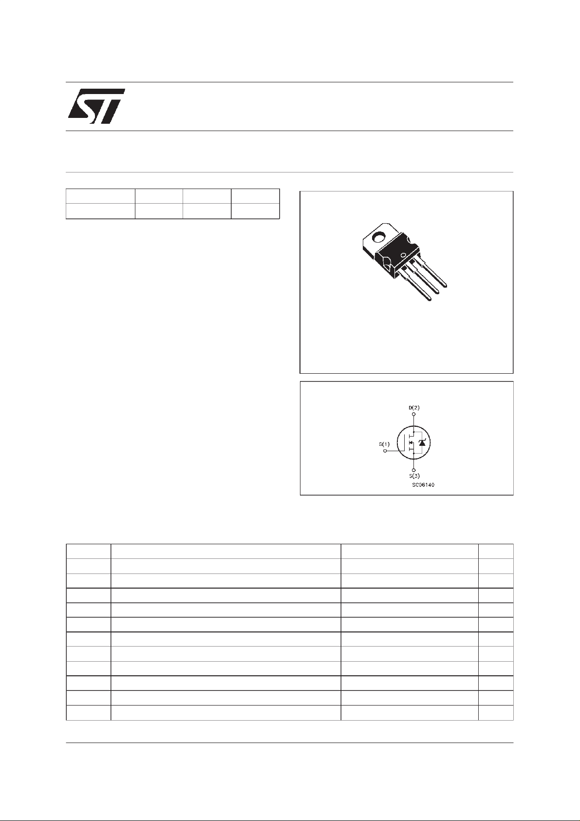
3
2
1
TO-220
INTERNAL SCHEMATIC DIAGRAM
ABSOLUTE MAXIMUM RATINGS
Symb o l Para meter Value Uni t
V
V
V
I
DM
P
dv/ dt (
T
(•) Pulse width limitedby safe operating area (1)ISD≤ 20 A,di/dt ≤ 300A/µs, VDD≤ V
July 1998
Drain-source Volt age (VGS=0) 100 V
DS
DGR Drain- gate Voltage (R
Gat e- source Voltage ± 20 V
GS
I
Drain C ur rent (continuous) at Tc=25oC20A
D
I
Drain C ur rent (continuous) at Tc=100oC14A
D
=20kΩ)
GS
100 V
(•) Dra in Current (pulsed) 80 A
Tot al Dis sipation at Tc=25oC90W
tot
Derating Factor 0.6 W/
1) Peak Diode Recover y v o lt age slope 7 V/ns
Sto rage T em pe r ature -65 to 17 5
stg
T
Max. O perating J u nc tion Temperat u r e 175
j
(BR)DSS,Tj≤TJMAX
o
C
o
C
o
C
1/8
Page 2
STP20NE10
THERMAL DATA
R
thj-case
Rthj-amb
R
thc-sin k
T
AVALANCHE CHARACTERISTICS
Symbol Para met e r Max Va lu e Uni t
I
AR
E
Ther mal Resist ance Junction- ca s e Max
Ther mal Resist ance Junction- ambient Max
Ther mal Resist ance Case-sink Typ
Maximum Lead Te mperat u re For Soldering P ur p os e
l
Avalanche C ur re nt , R epetiti ve or Not -Repetit ive
(pulse w idth limited b y T
Single Pulse Avalanche Energy
AS
(starting T
=25oC, ID=IAR,VDD=30V)
j
max, δ <1%)
j
1.67
62.5
0.5
300
20 A
170 mJ
o
C/W
oC/W
o
C/W
o
C
ELECTRICAL CHARACTERISTICS (T
=25oC unlessotherwise specified)
case
OFF
Symbol Parameter Te st Cond itions Min. Typ. Max. Unit
V
(BR)DSS
Drain-source
=250µAVGS=0
I
D
100 V
Breakdown V oltage
I
DSS
I
GSS
Zer o G at e Voltage
Drain Current ( V
GS
Gat e-body Leakage
Current (V
DS
=0)
=0)
=MaxRating
V
DS
V
=MaxRating Tc=125
DS
o
C
= ± 20 V
V
GS
1
10
± 100 nA
ON (∗)
Symbol Parameter Te st Cond itions Min. Typ. Max. Unit
V
GS(th )
Gate Threshold
V
DS=VGSID
=250µA
234V
Voltage
R
DS(on)
Stati c Drain-so urce O n
VGS=10V ID= 10 A 0.07 0.1 Ω
Resistance
I
D(on)
On S tate Drain Cu r re nt VDS>I
D(on)xRDS(on)max
20 A
VGS=10V
DYNAMIC
Symbol Parameter Te st Cond itions Min. Typ. Max. Unit
g
(∗)Forward
fs
Tr ansconductance
C
C
C
Input Ca pac i t an c e
iss
Out put Capa c itance
oss
Reverse T ransfer
rss
Capa cit an c e
VDS>I
D(on)xRDS(on)maxID
=10 A 6 S
VDS=25V f=1MHz VGS= 0 1600
180
50
2100
250
70
µA
µA
pF
pF
pF
2/8
Page 3
STP20NE10
ELECTRICAL CHARACTERISTICS (continued)
SWITCHINGON
Symbol Parameter Te st Cond itions Min. Typ. Max. Unit
t
d(on)
Turn-on Tim e
r
Rise T ime
t
VDD=30V ID=10A
=4.7 Ω VGS=10V
R
G
17
37
(see test circuit, figure 3)
Q
Q
Q
Total Gate Charge
g
Gat e-Sourc e Cha r ge
gs
Gate-Drain Charge
gd
VDD=80V ID=20A VGS=10V 38
10
12
SWITCHINGOFF
Symbol Parameter Te st Cond itions Min. Typ. Max. Unit
t
r(Voff)
t
t
Of f - voltage Ris e Time
Fall Time
f
Cross-over Time
c
VDD=80V ID=20A
=4.7 Ω VGS=10V
R
G
(see test circuit, figure 5)
11
18
32
SOURCE DRAIN DIODE
Symbol Parameter Te st Cond itions Min. Typ. Max. Unit
I
SD
I
SDM
V
SD
t
Q
I
RRM
(∗) Pulsed: Pulse duration =300 µs,duty cycle 1.5 %
(•) Pulse width limited by safe operating area
Source-drain Cu rrent
(•)
Source-drain Cu rrent
(pulsed)
(∗) For ward O n V o lt age ISD=20A VGS=0 1.5 V
Reverse Recovery
rr
Time
Reverse Recovery
rr
= 20 A di/dt = 10 0 A /µ s
I
SD
=30V Tj=150oC
V
DD
(see test circuit, figure 5)
110
440
Charge
Reverse Recovery
8
Current
23
50
50 nC
15
25
44
16
64
ns
ns
nC
nC
ns
ns
ns
A
A
ns
µC
A
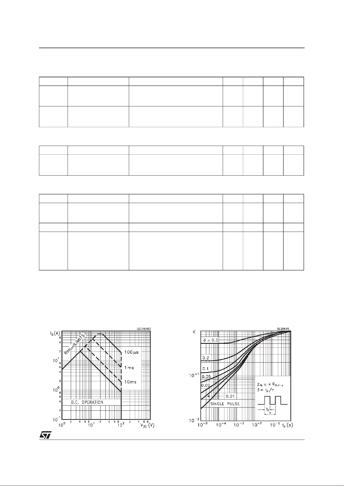
Safe Operating Area ThermalImpedance
3/8
Page 4

STP20NE10
OutputCharacteristics
Transconductance
TransferCharacteristics
StaticDrain-sourceOn Resistance
GateCharge vs Gate-sourceVoltage
4/8
CapacitanceVariations
Page 5

STP20NE10
Normalized GateThresholdVoltage vs
Temperature
Source-drainDiode Forward Characteristics
Normalized On Resistancevs Temperature
5/8
Page 6

STP20NE10
Fig. 1: Unclamped InductiveLoad Test Circuit
Fig. 3: SwitchingTimes Test CircuitsFor
ResistiveLoad
Fig. 2: Unclamped Inductive Waveform
Fig. 4: Gate Chargetest Circuit
Fig. 5: Test Circuit For InductiveLoad Switching
And Diode RecoveryTimes
6/8
Page 7

TO-220 MECHANICAL DATA
STP20NE10
DIM.
MIN. TYP. MAX. MIN. TYP. MAX.
A 4.40 4.60 0.173 0.181
C 1.23 1.32 0.048 0.051
D 2.40 2.72 0.094 0.107
D1 1.27 0.050
E 0.49 0.70 0.019 0.027
F 0.61 0.88 0.024 0.034
F1 1.14 1.70 0.044 0.067
F2 1.14 1.70 0.044 0.067
G 4.95 5.15 0.194 0.203
G1 2.4 2.7 0.094 0.106
H2 10.0 10.40 0.393 0.409
L2 16.4 0.645
L4 13.0 14.0 0.511 0.551
L5 2.65 2.95 0.104 0.116
L6 15.25 15.75 0.600 0.620
L7 6.2 6.6 0.244 0.260
L9 3.5 3.93 0.137 0.154
DIA. 3.75 3.85 0.147 0.151
mm inch
E
A
L4
D
F2
F1
G1
F
H2
G
C
D1
L2
Dia.
L5
L7
L6
L9
P011C
7/8
Page 8

STP20NE10
Information furnished is believed tobe accurate and reliable. However, STMicroelectronicsassumes no responsibility for the consequences
of use of such information nor for any infringement of patents or other rights of third parties which may resultfrom its use. No license is
granted by implication orotherwise under any patent or patentrights of STMicroelectronics. Specification mentioned in this publication are
subject tochange without notice. This publication supersedes and replaces allinformation previously supplied.STMicroelectronics products
are not authorized for use as critical componentsin life support devices or systems withoutexpresswritten approval of STMicroelectronics.
Australia - Brazil - Canada - China- France- Germany- Italy - Japan - Korea- Malaysia - Malta - Mexico - Morocco- The Netherlands -
Singapore- Spain- Sweden- Switzerland- Taiwan-Thailand - United Kingdom- U.S.A.
The ST logo isa trademark of STMicroelectronics
1998 STMicroelectronics– Printed in Italy – All Rights Reserved
STMicroelectronicsGROUP OF COMPANIES
.
8/8
 Loading...