

Page 1
STP20NE06
N - CHANNEL 60V - 0.06 Ω - 20A TO-220/TO-220FP
TYPE V
ST P20NE06
ST P20NE06FP
■ TYPICALR
■ EXCEPTIONALdv/dtCAPABILITY
■ 100%AVALANCHETESTED
■ LOW GATE CHARGE 100
■ APPLICATIONORIENTED
DS(on)
DSS
60 V
60 V
= 0.06 Ω
CHARACTERIZATION
DESCRIPTION
This Power Mosfet is the latest development of
STMicroelectronics unique ” Single Feature
Size ” strip-basedprocess. The resulting transi-
stor shows extremelyhigh packing densityforlow
on-resistance, rugged avalance characteristics
and less critical alignment steps therefore a remarkablemanufacturingreproducibility.
R
DS(on)
<0.080Ω
<0.080Ω
o
C
I
D
20 A
13 A
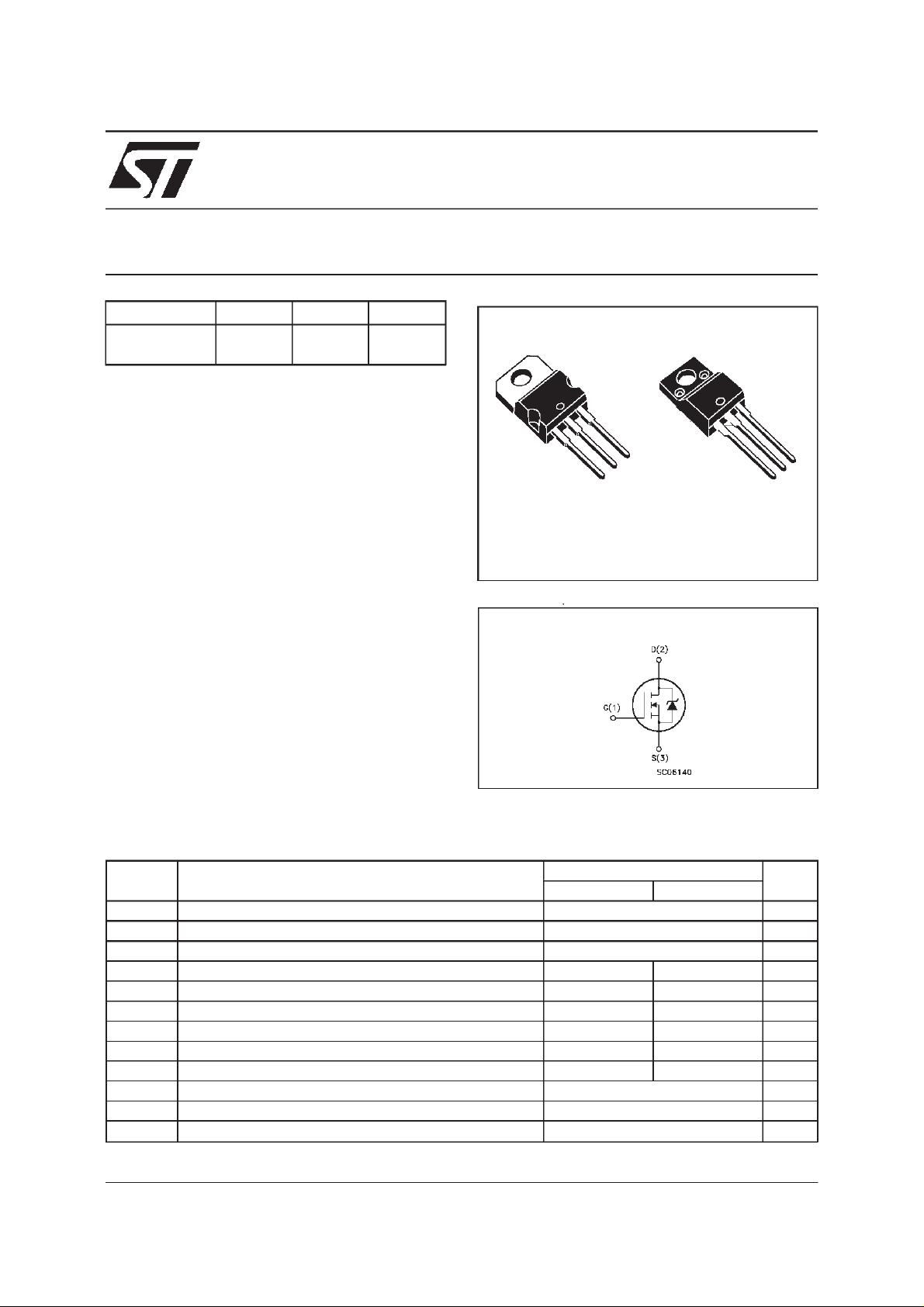
STP20NE06FP
STripFET POWER MOSFET
3
2
1
TO-220 TO-220FP
INTERNAL SCHEMATIC DIAGRAM
3
2
1
APPLICATIONS
■ HIGHCURRENT, HIGH SPEEDSWITCHING
■ SOLENOIDAND RELAY DRIVERS
■ MOTORCONTROL, AUDIOAMPLIFIERS
■ DC-DC& DC-AC CONVERTERS
■ AUTOMOTIVEENVIRONMENT(INJECTION,
ABS, AIR-BAG, LAMPDRIVERS,Etc.)
ABSOLUTE MAXIMUM RATINGS
Symbol Parameter Value Unit
ST P20NE06 STP20NE06FP
V
V
V
I
DM
P
V
dv/ dt P ea k Diode Recover y volt age slope 7 V/ ns
T
(•) Pulse width limited by safe operating area (1)ISD≤ 20 A, di/dt ≤ 300 A/µs, VDD≤ V
June 1999
Drain-source Voltage (VGS=0) 60 V
DS
Drain- gate Vol t age (RGS=20kΩ)60V
DGR
Gate-source Voltage ± 20 V
GS
I
Drain Curre nt (cont i nuous) at Tc=25oC2013A
D
Drain Curre nt (cont i nuous) at Tc=100oC149A
I
D
(•) Drain Curre nt (pulse d) 80 80 A
Total Dissipation at Tc=25oC7030W
tot
Derat ing F ac tor 0.47 0.2 W/
Ins ulat ion W i th s t and Voltage ( DC) 2000 V
ISO
Sto rage Temper at ur e -65 to 175
stg
T
Max. Operat ing Junct ion Tem pe ra ture 175
j
(BR)DSS,Tj≤TJMAX
o
C
o
C
o
C
1/9
Page 2
STP20NE06/FP
THERMAL DATA
TO-220 TO-220FP
R
thj-case
R
thj-amb
R
thc-sink
T
AVALANCHE CHARACTERISTICS
Symbol Parameter Max V alue Unit
I
AR
E
Ther mal Resistanc e Junct ion-case M a x 2.14 5
Ther mal Resistanc e Junct ion-ambie nt Max
Ther mal Resistanc e Case-sink Ty p
Maximum Lead Tempe ra tur e F or S o ldering Purpos e
l
Avalanche Current, R epetitive or Not-Repetitive
(pulse width limited by T
Single Pul se Avalanc he Ener gy
AS
(starting T
=25oC, ID=IAR,VDD=25V)
j
max)
j
62.5
0.5
300
20 A
100 mJ
o
C/W
o
C/W
o
C/W
o
C
ELECTRICAL CHARACTERISTICS
=25oC unless otherwisespecified)
(T
case
OFF
Symbol Parameter Test Conditions Min. Typ. Max. Unit
V
(BR)DSS
Drain-source
ID=250µAVGS=0 60 V
Break dow n Vo lt age
I
DSS
I
GSS
Zero Gate Volta ge
Drain Curre nt (V
GS
Gat e- bod y Leakag e
Current (V
DS
=0)
=0)
V
=MaxRating
DS
=MaxRating Tc= 125oC
V
DS
V
=± 20 V
GS
1
10
100 nA
±
ON(∗)
Symbol Parameter Test Conditions Min. Typ. Max. Unit
V
GS(th)
R
DS(on)
Gate Threshold Voltage VDS=VGSID= 250µA 234V
Sta t ic Drain-s our c e On
VGS=10V ID= 10 A 0.060 0.080
Resistance
I
D(on)
On State Drain Current VDS>I
D(on)xRDS(on)max
20 A
VGS=10V
DYNAMIC
Symbol Parameter Test Conditions Min. Typ. Max. Unit
g
(∗)Forward
fs
Tr ansc on duc tance
C
C
C
Input Capaci t ance
iss
Out put Capac itance
oss
Reverse Transfer
rss
Capacit a nc e
VDS>I
D(on)xRDS(on)maxID
=10 A 5 9 S
VDS=25V f=1MHz VGS= 0 900
125
35
µA
µA
Ω
pF
pF
pF
2/9
Page 3
STP20NE06/FP
ELECTRICAL CHARACTERISTICS
(continued)
SWITCHING ON
Symbol Parameter Test Conditions Min. Typ. Max. Unit
t
d(on)
t
Tur n-on Delay T ime
Rise Time
r
VDD=30V ID=10A
R
G
=4.7
Ω
VGS=10V
20
45
(see test circuit, figure 3)
Q
Q
Q
Tot al Gate Charge
g
Gat e- Source Charg e
gs
Gate-Drain Charge
gd
VDD=48V ID=20A VGS=10V 25
10
6
35 nC
SWITCHING OFF
Symbol Parameter Test Conditions Min. Typ. Max. Unit
t
r(Voff)
t
t
Off-v oltage Rise Time
Fall T ime
f
Cross-over T im e
c
VDD=48V ID=20A
=4.7 Ω VGS=10V
R
G
(see test circuit, figure 5)
8
25
37
SOURCEDRAINDIODE
Symbol Parameter Test Conditions Min. Typ. Max. Unit
I
SD
I
SDM
V
SD
t
Q
I
RRM
(∗) Pulsed:Pulse duration= 300µs, duty cycle 1.5%
(•) Pulse width limited by safe operatingarea
Source-drain Current
(•)
Source-drain Current
20
80
(pulsed)
(∗)ForwardOnVoltage ISD=20A VGS=0 1.5 V
Reverse Recovery
rr
Time
Reverse Recovery
rr
ISD= 20 A di/dt = 100 A/µs
=30V Tj= 150oC
V
DD
(see test circuit, figure 5)
50
115
Charge
Reverse Recovery
4.5
Current
ns
ns
nC
nC
ns
ns
ns
A
A
ns
nC
A
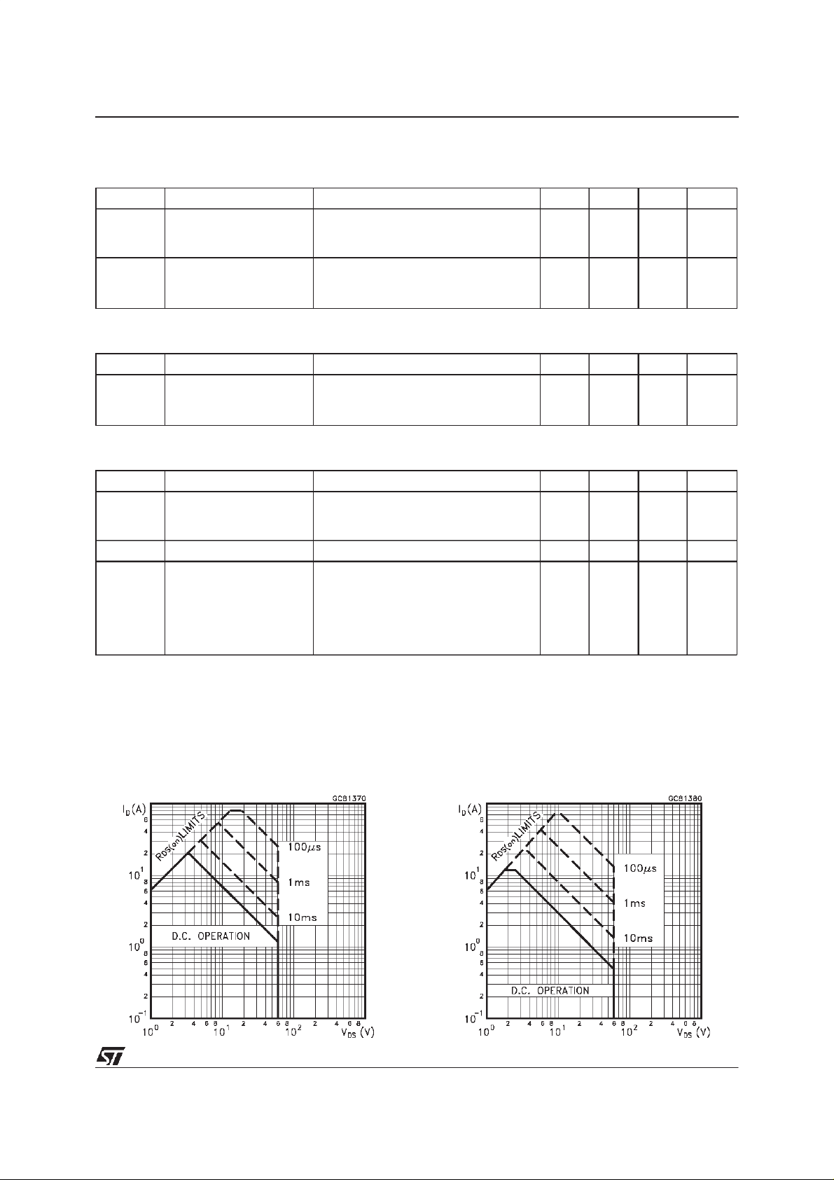
SafeOperating Area for TO-220 SafeOperating Area for TO-220FP
3/9
Page 4

STP20NE06/FP
ThermalImpedancefor TO-220
OutputCharacteristics
ThermalImpedanceforTO-220FP
TransferCharacteristics
Transconductance
4/9
Static Drain-sourceOn Resistance
Page 5

STP20NE06/FP
Gate Charge vs Gate-sourceVoltage
NormalizedGate ThresholdVoltage vs
Temperature
CapacitanceVariations
NormalizedOn Resistancevs Temperature
Source-drainDiode Forward Characteristics
5/9
Page 6

STP20NE06/FP
Fig. 1:
UnclampedInductiveLoad Test Circuit
Fig. 3: SwitchingTimes Test Circuits For
ResistiveLoad
Fig. 2:
UnclampedInductive Waveform
Fig. 4: Gate Chargetest Circuit
Fig. 5:
Test Circuit For InductiveLoad Switching
And Diode Recovery Times
6/9
Page 7

TO-220 MECHANICAL DATA
STP20NE06/FP
DIM.
MIN. TYP. MAX. MIN. TYP. MAX.
A 4.40 4.60 0.173 0.181
C 1.23 1.32 0.048 0.051
D 2.40 2.72 0.094 0.107
D1 1.27 0.050
E 0.49 0.70 0.019 0.027
F 0.61 0.88 0.024 0.034
F1 1.14 1.70 0.044 0.067
F2 1.14 1.70 0.044 0.067
G 4.95 5.15 0.194 0.203
G1 2.4 2.7 0.094 0.106
H2 10.0 10.40 0.393 0.409
L2 16.4 0.645
L4 13.0 14.0 0.511 0.551
L5 2.65 2.95 0.104 0.116
L6 15.25 15.75 0.600 0.620
L7 6.2 6.6 0.244 0.260
L9 3.5 3.93 0.137 0.154
DIA. 3.75 3.85 0.147 0.151
mm inch
E
A
L4
D
F2
F1
G1
H2
G
F
P011C
C
D1
L2
Dia.
L5
L7
L6
L9
7/9
Page 8

STP20NE06/FP
TO-220FP MECHANICAL DATA
DIM.
MIN. TYP. MAX. MIN. TYP. MAX.
A 4.4 4.6 0.173 0.181
B 2.5 2.7 0.098 0.106
D 2.5 2.75 0.098 0.108
E 0.45 0.7 0.017 0.027
F 0.75 1 0.030 0.039
F1 1.15 1.7 0.045 0.067
F2 1.15 1.7 0.045 0.067
G 4.95 5.2 0.195 0.204
G1 2.4 2.7 0.094 0.106
H 10 10.4 0.393 0.409
L2 16 0.630
L3 28.6 30.6 1.126 1.204
L4 9.8 10.6 0.385 0.417
L6 15.9 16.4 0.626 0.645
L7 9 9.3 0.354 0.366
Ø 3 3.2 0.118 0.126
mm inch
E
A
D
B
L3
L6
L7
¯
F1
F
G1
H
G
F2
123
L2
L4
8/9
Page 9

STP20NE06/FP
Information furnished is believed tobe accurate and reliable. However, STMicroelectronics assumes no responsibility for the consequences
of use of such information nor for any infringement of patents or other rights of third parties which may result from its use. No license is
granted by implication orotherwise under any patent or patent rights of STMicroelectronics. Specificationmentioned in this publication are
subjecttochange without notice. This publication supersedes andreplaces all information previously supplied. STMicroelectronicsproducts
are not authorized for use as critical components in life support devices or systemswithout express written approval of STMicroelectronics.
The STlogo is a trademark of STMicroelectronics
1999 STMicroelectronics – Printed in Italy – All Rights Reserved
STMicroelectronics GROUP OF COMPANIES
Australia - Brazil - China - Finland - France - Germany - Hong Kong - India - Italy - Japan - Malaysia - Malta - Morocco -
Singapore - Spain - Sweden - Switzerland - United Kingdom - U.S.A.
http://www.st.com
.
9/9
 Loading...