

Page 1
STP20N20
STF20N20 - STD20N20
N-CHANNEL 200V - 0.10Ω - 18A TO-220/TO-220FP/DPAK
LOW GATE CHARGE STripFET™ II MOSFET
Table 1: Ge neral Features
TYPE V
STD20N20
STF20N20
STP20N20
■ TYPICAL R
■ EXCEPTIONAL dv/dt CAPABILITY
■ LOW GATE CHARGE
■ 100% AVALANCHE TESTED
DSS
200 V
200 V
200 V
(on) = 0.10 Ω
DS
R
DS(on)
< 0.125 Ω
< 0.125 Ω
< 0.125 Ω
I
d
18 A
18 A
18 A
P
TOT
90 W
25 W
90 W
DESCRIPTION
This MOSFET series realized with STMicroelectronics unique S TripFET process has specifically
been designed to minim ize i nput c apacitance a nd
gate charge. It is therefore suitable as primary
switch in advanced high-efficiency isolated DC-DC
converters.
APPLICATIONS
■ HIGH CURRENT SWITCHING
APPLICATIONS
■ HIGH EFFICIENCY DC-DC CONVERTERS
■ PRIMARY SIDE SWITCH
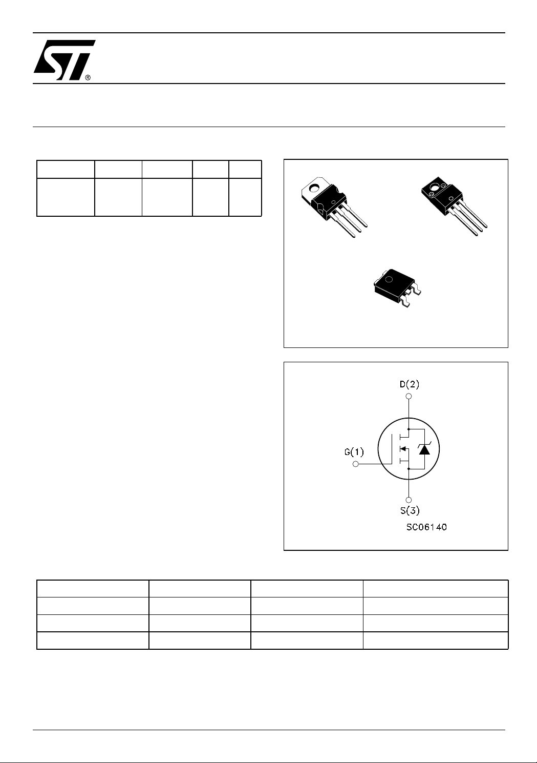
Figure 1: Package
3
2
1
TO-220
TO-220FP
3
1
DPAK
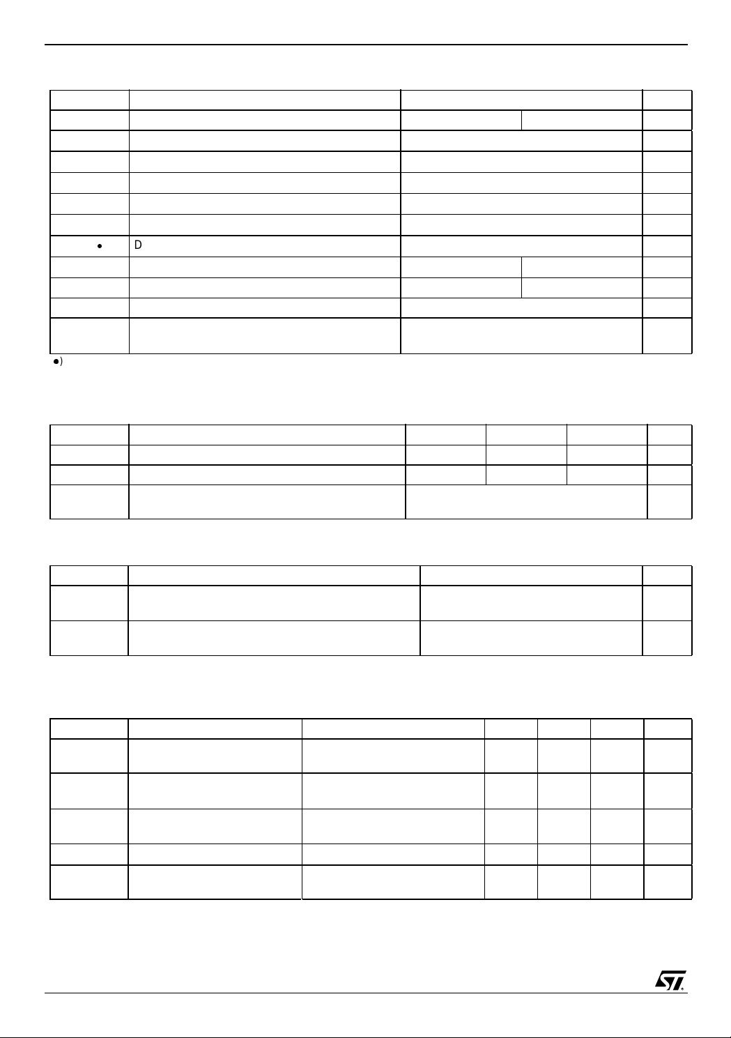
Figure 2: Internal Schematic Diagram
3
2
1
Table 2: Order Codes
SALES TYPE MARKING PACKAGE PACKAGING
STD20N20T4 D20N20 DPAK TAPE & REEL
STF20N20 F20N20 TO-220FP TUBE
STP20N20 P20N20 TO-220 TUBE
Rev. 3
1/13January 2005
Page 2
STP20N20 - STF20N20 - STD20N20
Table 3: Absolute Maximum ratings
Symbol Parameter Value Unit
TO-220/DPAK TO-220FP
V
DS
V
DGR
V
GS
I
D
I
D
I
DM
P
TOT
dv/dt (1) Peak Diode Recovery voltage slope 15 V/ns
T
j
T
stg
() Pulse wi dt h l i m i ted by safe operating area
(1) I
≤ 18A, di/dt ≤ 400A/µs, VDD ≤ V
SD
Table 4: Thermal Data
Rthj-case Thermal Resistance Junction-case Max 1.38 1.38 5 °C/W
Rthj-amb Thermal Resistance Junction-ambient Max 62.5 50(#) 62.5 °C/W
T
l
(#) When mounted on 1inch² FR-4, 2 Oz copper board.
Drain-source Voltage (VGS = 0) 200 V
Drain-gate Voltage (RGS = 20 kΩ)200V
Gate- source Voltage
± 20 V
Drain Current (continuous) at TC = 25°C18A
Drain Current (continuous) at TC = 100°C11A
()
Drain Current (pulsed)
72 A
Total Dissipation at TC = 25°C9025W
Derating Factor 0.72 0.2 W/°C
Operating Junction Temperature
Storage Temperature
(BR)DSS
-50 to 150 °C
TO-220 DPAK TO-220FP
Maximum Lead Temperature For Soldering
300 °C
Purpose
Table 5: Avalanche Characteristics
Symbol Parameter Max Value Unit
I
AR
E
AS
Avalanche Current, Repetitive or Not-Repetitive
(pulse width limited by T
max)
j
Single Pulse Avalanche Energy
(starting T
= 25 °C, ID = IAR, VDD = 50 V)
j
ELECTRICAL CHARACTERISTICS (T
=25°C UNLESS OTHERWISE SPECIFIED)
CASE
18 A
110 mJ
Table 6: On/Off
Symbol Parameter Test Conditions Min. Typ. Max. Unit
V
(BR)DSS
I
DSS
I
GSS
V
GS(th)
R
DS(on)
Drain-source
Breakdown Voltage
Zero Gate Voltage
Drain Current (V
GS
= 0)
Gate-body Leaka ge
Current (V
DS
= 0)
Gate Threshold Voltage
Static Drain-source On
Resistance
ID = 1 mA, VGS = 0 200 V
= Max Rating
V
DS
V
= Max Rating, TC = 125 °C
DS
V
= ± 20V ±100 nA
GS
V
= VGS, ID = 250 µA 2 3 4 V
DS
1
10
VGS = 10V, ID = 10 A 0.10 0.125 Ω
µA
µA
2/13
Page 3
STP20N20 - STF20N20 - STD20N20
ELECTRICAL CHARACTERISTICS (CONTINUED)
Table 7: Dynamic
Symbol Parameter Test Conditions Min. Typ. Max. Unit
(1)
g
C
C
t
t
fs
C
iss
oss
rss
d(on)
t
r
d(off)
t
r
Q
Q
gs
Q
gd
g
Forward Transconductance
Input Capacitance
Output Capacitance
Reverse Transfer
Capacitance
Turn-on Delay Time
Rise Time
Turn-off Delay Time
Fall Time
Total Gate Charge
Gate-Source Charge
Gate-Drain Charge
Table 8: Source Drain Diode
Symbol Parameter Test Conditions Min. Typ. Max. Unit
I
SD
I
(2)
SDM
VSD (1)
t
rr
Q
rr
I
RRM
t
rr
Q
rr
I
RRM
(1) Pulsed: Pulse durat ion = 300 µs, duty cycle 1.5 %.
(2) Pulse width limite d by safe operatin g area.
Source-drain Current
Source-drain Current (pulsed)
Forward On Voltage
Reverse Recovery Time
Reverse Recovery Charge
Reverse Recovery Current
Reverse Recovery Time
Reverse Recovery Charge
Reverse Recovery Current
VDS = 25 V, ID= 10 A 13 S
= 25V, f = 1 MHz, VGS = 0 940
V
DS
197
30
= 100 V, ID = 10 A,
V
DD
RG= 4.7 Ω VGS = 10 V
(see Figure 17)
15
30
40
10
= 160V, ID = 20 A,
V
DD
VGS = 10V
(see Figure 20)
28
5.6
14.5
39 nC
18
72
ISD = 20 A, VGS = 0 1.6 V
= 20 A, di/dt = 100A/µs
I
SD
VDD = 50V, Tj = 25°C
(see Figure 18)
= 20 A, di/dt = 100A/µs
I
SD
VDD = 50V, Tj = 150°C
(see Figure 18)
155
775
10
183
1061
11.6
pF
pF
pF
ns
ns
ns
ns
nC
nC
A
A
ns
nC
A
ns
nC
A
3/13
Page 4
STP20N20 - STF20N20 - STD20N20
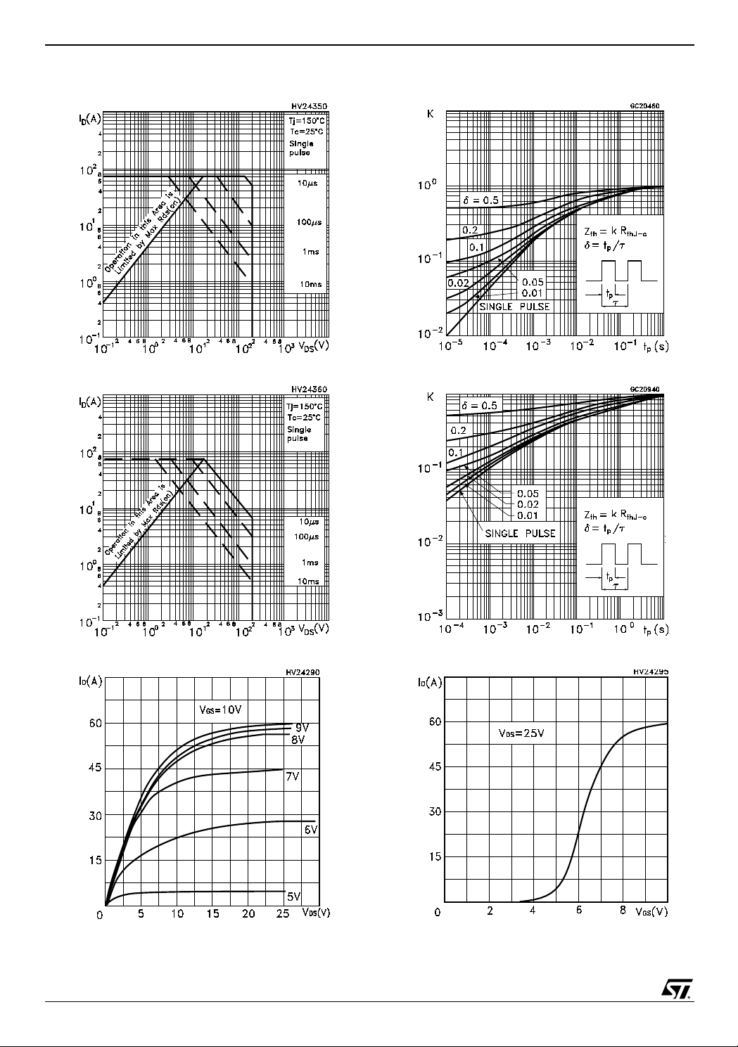
Figure 3: Safe Operating Area For TO-220/ DPAK
Figure 4: Safe Operating Area For TO-220FP
Figure 6: Thermal Impedance For TO-220/ DPAK
Figure 7: Thermal Impedance For TO-220FP
Figure 5: Output Characteristics
4/13
Figure 8: Transfer Characteristics
Page 5

STP20N20 - STF20N20 - STD20N20
Figure 9: Transconductance
Figure 10: Gate Charge vs Gate-source Voltage
Figure 12: Static Drain-source On Resistance
Figure 13: Capacitance Variations
Figure 11: Normalized Gate Threshold Voltage vs Tem perature
Figure 14: Normal ized On R esistance vs Temperature
5/13
Page 6

STP20N20 - STF20N20 - STD20N20
Figure 15: S ource-Drain Forward Char acteristics
6/13
Page 7

STP20N20 - STF20N20 - STD20N20
Figure 16: Unclamped Inductive Load Test Circuit
Figure 17: Switching Times Test Circuit For Resistive Load
Figure 19: Unclamped Inductive Wafeform
Figure 20: Gate Charge Test Circuit
Figure 18: Test Circuit For Inductive Load Switching and Diode Recovery Times
7/13
Page 8

STP20N20 - STF20N20 - STD20N20
TO-220 MECHANICAL DATA
DIM.
A 4.40 4.60 0.173 0.181
b 0.61 0.88 0.024 0.034
b1 1.15 1.70 0.045 0.066
c 0.49 0.70 0.019 0.027
D 15.25 15.75 0.60 0.620
E 10 10.40 0.393 0.409
e 2.40 2.70 0.094 0.106
e1 4.95 5.15 0.194 0.202
F 1.23 1.32 0.048 0.052
H1 6.20 6.60 0.244 0.256
J1 2.40 2.72 0.094 0.107
L 13 14 0.511 0.551
L1 3.50 3.93 0.137 0.154
L20 16.40 0.645
L30 28.90 1.137
øP 3.75 3.85 0.147 0.151
Q 2.65 2.95 0.104 0.116
MIN. TYP MAX. MIN. TYP. MAX.
mm. inch
8/13
Page 9

STP20N20 - STF20N20 - STD20N20
TO-220FP MECHANICAL DATA
DIM.
A 4.4 4.6 0.173 0.181
B 2.5 2.7 0.098 0.106
D 2.5 2.75 0.098 0.108
E 0.45 0.7 0.017 0.027
F 0.75 1 0.030 0.039
F1 1.15 1.7 0.045 0.067
F2 1.15 1.7 0.045 0.067
G 4.95 5.2 0.195 0.204
G1 2.4 2.7 0.094 0.106
H 10 10.4 0.393 0.409
L2 16 0.630
L3 28.6 30.6 1.126 1.204
L4 9.8 10.6 .0385 0.417
L5 2.9 3.6 0.114 0.141
L6 15.9 16.4 0.626 0.645
L7 9 9.3 0.354 0.366
Ø 3 3.2 0.118 0.126
MIN. TYP MAX. MIN. TYP. MAX.
mm. i nch
E
A
D
B
L3
L6
L7
F1
F
G1
H
G
F2
123
L2
L5
L4
9/13
Page 10

STP20N20 - STF20N20 - STD20N20
TO-252 (DPAK) MECHANICAL DATA
DIM.
A 2.20 2.40 0.087 0.094
A1 0.90 1.10 0.035 0.043
A2 0.03 0.23 0.001 0.009
B 0.64 0.90 0.025 0.035
B2 5.20 5.40 0.204 0.213
C 0.45 0.60 0.018 0.024
C2 0.48 0.60 0.019 0.024
D 6.00 6.20 0.236 0.244
E 6.40 6.60 0.252 0.260
G 4.40 4.60 0.173 0.181
H 9.35 10.10 0.368 0.398
L2 0.8 0.031
L4 0.60 1.00 0.024 0.039
V2 0
MIN. TYP. MAX. MIN. TYP. MAX.
o
mm inch
o
8
o
0
o
0
10/13
P032P_B
Page 11

STP20N20 - STF20N20 - STD20N20
DPAK FOOTPRINT
All dimensions are in millimeters
TAPE AND REEL SHIPMENT (suffix ”T4”)*
TUBE SHIPMENT (no suffix)*
All dimensions
are in millimeters
REEL MECHANICAL DATA
DIM.
A 330 12. 992
B 1.5 0.059
C 12.8 13.2 0.504 0.520
D 20.2 0.795
G 16.4 18.4 0.645 0.724
N 50 1.968
T 22.4 0.881
mm inch
MIN. MAX. MIN. MAX.
TAPE MECHANICAL DATA
DIM.
A0 6.8 7 0.267 0.275
B0 10.4 10.6 0.409 0.417
B1 12.1 0.476
D 1.5 1.6 0.059 0.063
D1 1.5 0.059
E 1.65 1.85 0.065 0.073
F 7.4 7.6 0.291 0.299
K0 2.55 2.75 0.100 0.108
P0 3.9 4.1 0.153 0.161
P1 7.9 8.1 0.311 0.319
P2 1.9 2.1 0.075 0.082
R 40 1.574
W 15.7 16.3 0.618 0.641
* on sales type
mm inch
MIN. MAX. MIN. MAX.
BASE QTY BULK QTY
2500 2500
11/13
Page 12

STP20N20 - STF20N20 - STD20N20
Table 9: Revision History
Date R evisio n Descrip tion of Change s
06-Dec-2004 1 Data Brief
07-Dec-2004 2 First Revision
12-Jan-2005 3 Final datasheet
12/13
Page 13

STP20N20 - STF20N20 - STD20N20
Information furnished is believed to be accurate and reliable. However, STMicroelectronics assumes no responsibility for the consequences
of use of such information nor for any infringement of patents or other rights of third parties which may result from its use. No license is g ranted
by implic ati o n or ot h er wis e und er an y pat ent or pa te nt r igh ts of STMi cr oe l ect ro ni cs . Sp ec if i cat i on s ment i o ned i n th is p ub li c ati on ar e s ubj ec t
to change without notice. This public ation supersedes and replaces all information previously supplie d. STMicroelectronics pro ducts are not
authorized for use as critical components in life support devices or systems without express written approval of STMicroelectronics.
The ST logo is a registered trademark of STMicroelectronics
All other names are the property of their respective owners
© 2005 STMicroelectronics - All Rights Reserved
STMicroelectronics group of companies
Australia - Belgium - Brazil - Canada - China - Czech Republic - Finland - France - Germany - Hong Kong - India - Israel - Italy - Japan -
Malaysia - Malta - Morocco - Singapore - Spain - Sweden - Switzerland - United Kingdom - United States of America
13/13
 Loading...